

VB921ZVFI
HIGH VOLTAGE IGNITION COIL DRIVER
TYPE V
VB921ZVFI
VB921ZVSP
n NO EXTERNAL COMPONENT REQUIRED
n INTEGRATED HIGH VOLTAGE CLAMP
n COIL CURRENT LIMIT INTERNALLY SET
n HIGH RUGGEDNESS
cl
340V 7.5A 2.5V
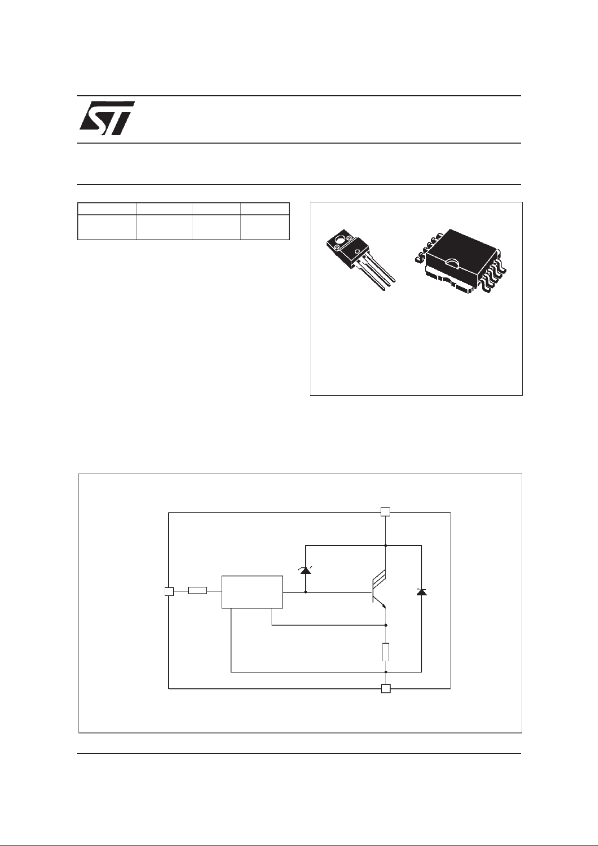
DESCRIPTION
The VB921ZVFI, VB921ZVSP is a monolithichigh
voltage integrated circuit made using the
STMicroelectronics VIPower technology, which
combines a vertical current flow power trilinton
with a coil current limiting circuit and a collector
voltage clamping. The device is particularly
suitable for application in high performance
electronic car ignition, where coil current limitation
and voltage clamping are required.
I
cl
V
cg(sat)
1
ISOWATT220
ORDER CODES:
ISOWATT220
POWERSO-10
/ VB921ZVSP
POWER I.C.
ADVANCED DATA
10
3
2
PowerSO-10
VB921ZVFI
VB921ZVSP
1
BLOCK DIAGRAM
HV
c
V
IN
July 1999 1/7
CONTROL
UNIT
R
SENSE
GND
ND8012
1
VB921ZVFI / VB921ZVSP
ABSOLUTE MAXIMUM RATING
Symbol Parameter
HV
I
V
I
IN
P
T
T
stg
THERMAL DATA
Symbol Parameter
R
thj-case
R
thj-amb
CONNECTION DIAGRAM (TOP VIEW)
Collector Voltage Internally limited V
c
Collector Current Internally limited A
C
Maximum Input Voltage 8 V
IN
Input current 10 mA
Total dissipation at TC=25°C 40 100 W
tot
Junction operating temperature - 40 to 150 °C
j
Storage temperature - 40 to 150 °C
Thermal resistance junction-case (MAX) 3.12 1.25 °C/W
Thermal resistance junction-ambient (MAX) 62.5 62.5 °C/W
Value
ISOWATT220 PowerSO-10
Value
ISOWATT220 PowerSO-10
Unit
Unit
V
IN
V
IN
V
IN
V
IN
V
IN
6
7
8
9
10
5
4
3
2
1
GND
GND
GND
GND
GND
3
2
1V
11
HV
C
ELECTRICAL CHARACTERISTICS (V
=12V; T
CC
=25ºC unless otherwisespecified)
case
Symbol Parameter Test Conditions Min Typ Max Unit
V
I
I
cgo
V
cl
I
cl
Input Voltage 4.2 5.5 V
IN
V
IN
Input Current
=4.2V; IC=5A (See test circuit)
IN
VIN=5V; IC=5A
5
10
Collector Cut-off Current VIN=0V; HVC=250V 250 µA
(*) High voltage clamp -40°C<Tj<125°C 340 440 V
(*) Coil Current Limit
V
=4.2V; -40°C<Tj<125°C
IN
=5V; -40°C<Tj<125°C
V
IN
6
6.5 7.5
(See note 1)
V
cg(sat)
V
∆I
f
Power Stage Saturation
Voltage
IC=5A; IIN=10mA 2.5 V
(**) Diode Forward Voltage If=10A 3.5 V
Coil current variation in
cl
respect to VIN=5V
VIN=4.5 ÷ 5.5V 200 mA
GND
HV
mA
mA
A
A
C
IN
(*) Coil data: primary resistance RC=0.4 ÷ 0.8Ω, primary inductance LC=6 ÷ 8mH
(**) Pulsed: pulse duration= 300µs, duty cycle=1.5%
NOTE 1: Iclis also controlled in respect to the variation of VINbetween 4.5 and 5.5V
2/7
1
VB921ZVFI / VB921ZVSP
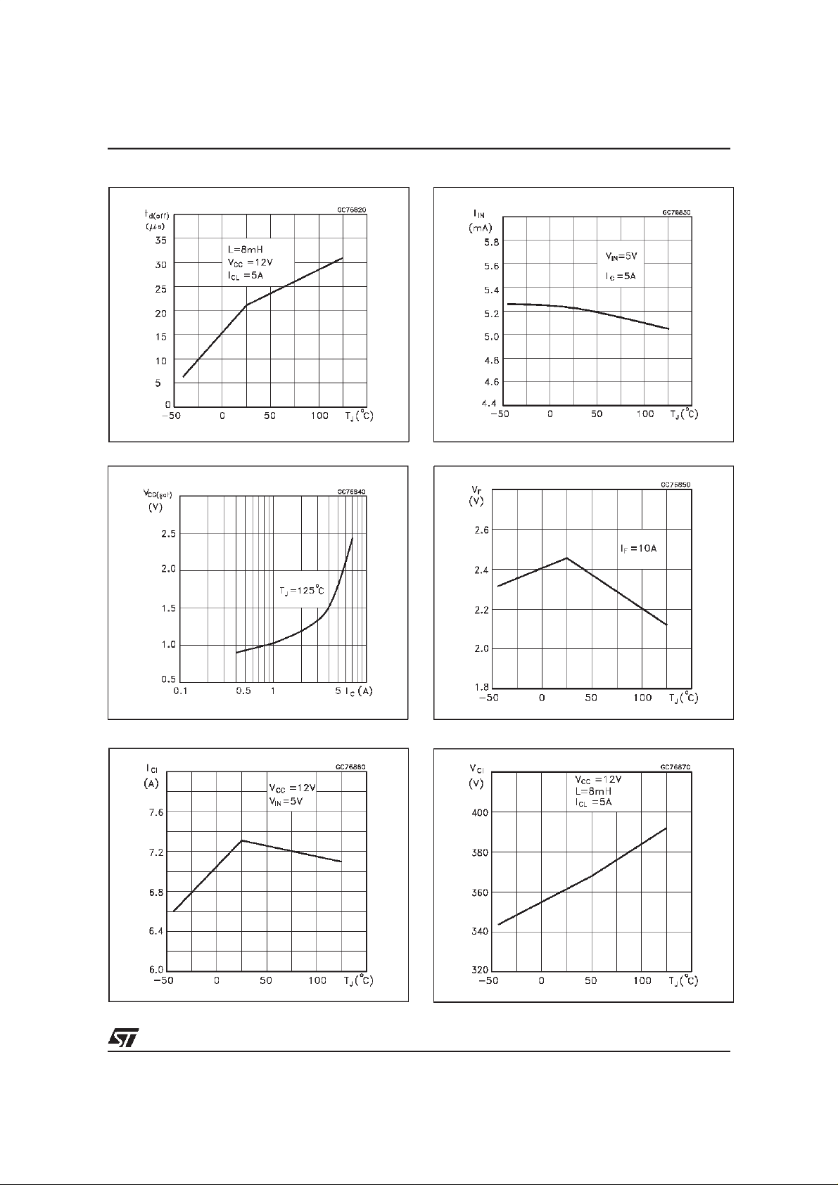
FIGURE 1: Delay-off time Vs Temperature
FIGURE 3: Saturation VoltageVS Collector Current
FIGURE 2: Input current Vs Temperature
FIGURE 4: Diode Forward Voltage VS Temperature
FIGURE 5: Coil Current Limit Vs Temperature
FIGURE 6: Clamping Voltage VS Temperature
3/7
11
1

VB921ZVFI / VB921ZVSP
FIGURE 7: Maximum Energy and Output Current
Unclamped
4/7
1
11
1

VB921ZVFI / VB921ZVSP
PowerSO-10 MECHANICAL DATA
DIM.
MIN. TYP MAX. MIN. TYP. MAX.
mm. inch
A 3.35 3.65 0.132 0.144
A1 0.00 0.10 0.000 0.004
B 0.40 0.60 0.016 0.024
c 0.35 0.55 0.013 0.022
D 9.40 9.60 0.370 0.378
D1 7.40 7.60 0.291 0.300
E 9.30 9.50 0.366 0.374
E1 7.20 7.40 0.283 0.291
E2 7.20 7.60 0.283 300
E3 6.10 6.35 0.240 0.250
E4 5.90 6.10 0.232 0.240
e 1.27 0.050
F 1.25 1.35 0.049 0.053
H 13.80 14.40 0.543 0.567
h 0.50 0.002
Q 1.70 0.067
α 0º 8º
B
B
Q
0.10 A
E1E3
==
SEATING
PLANE
A
C
α
E4
==
SEATING
PLANE
A1
L
==
==
==
HE
h
A
F
A1
610
51
eB
M
0.25
D
==
D1
==
E2
==
DETAIL”A”
DETAIL”A”
5/7
1

VB921ZVFI / VB921ZVSP
TO-220 MECHANICAL DATA
DIM.
MIN. TYP MAX. MIN. TYP. MAX.
A 4.40 4.60 0.173 0.181
C 1.23 1.32 0.048 0.051
D 2.40 2.72 0.094 0.107
D1 1.27 0.050
E 0.49 0.70 0.019 0.027
F 0.61 0.88 0.024 0.034
F1 1.14 1.70 0.044 0.067
F2 1.14 1.70 0.044 0.067
G 4.95 5.15 0.194 0.203
H2 10.0 10.40 0.393 0.409
L2 16.4 0.645
L4 13.0 14.0 0.511 0.551
L5 2.65 2.95 0.104 0.116
L6 15.25 15.75 0.600 0.620
L7 6.2 6.6 0.244 0.260
L9 3.5 3.93 0.137 0.154
DIA. 3.75 3.85 0.147 0.151
mm. inch
6/7
11
11111
1
1

VB921ZVFI / VB921ZVSP
Information furnished is believed to be accurate and reliable. However, STMicroelectronics assumes no responsibility for the consequences
of use of such information nor for any infringement of patents or other rights of third parties which may results from its use. No license is
granted by implication or otherwise under any patent or patent rightsof STMicroelectronics. Specifications mentioned in this publication are
subject to change without notice. This publication supersedes and replaces all information previously supplied. STMicroelectronics products
are not authorized for use as critical components in life support devices or systems without express written approval of STMicroelectronics.
Australia - Brazil - Canada - China - France - Germany - Italy - Japan - Korea - Malaysia - Malta - Mexico - Morocco -
The Netherlands- Singapore - Spain - Sweden - Switzerland - Taiwan- Thailand - United Kingdom - U.S.A.
The ST logo is a registered trademark of STMicroelectronics
1999 STMicroelectronics - Printed in ITALY- All Rights Reserved.
STMicroelectronics GROUPOF COMPANIES
7/7
1
 Loading...