

VB408
HIGH VOLTAGE LINEAR REGULATOR
TYPE
VB408
VB408FI
VB408B
■ INPUT VOLTAGEUP TO 400 V DC OR 285 V
RMS RECTIFIED
■ OUTPUTVOLTAGEADJUSTABLEFROM1.25
TO VIN-30V
■ OUTPUT CURRENT LIMITED TO 40 mA
■ THERMAL SHUT-DOWN PROTECTION
■ SHORT CIRCUIT PROTECTION
DESCRIPTION
The VB408, VB408B, VB408FI are fully protected
positive adjustable voltage regulators made using a
proprietary High Voltage VIPower technology. The
device can beconnected toa D.C. source (upto 400V) or
in off-line application directly to the rectified main (110V/
230V). It is particularly suitable to be used in the
manufacture of DC/DC converters, AC/DC converters,
∆V
IN,OUT
I
LIM
400 V 40 mA 1.25 to V
V
OUT
IN
-30 V
/ VB408B / VB408FI
POWER I.C.
PRELIMINARY DATA
3
2
1
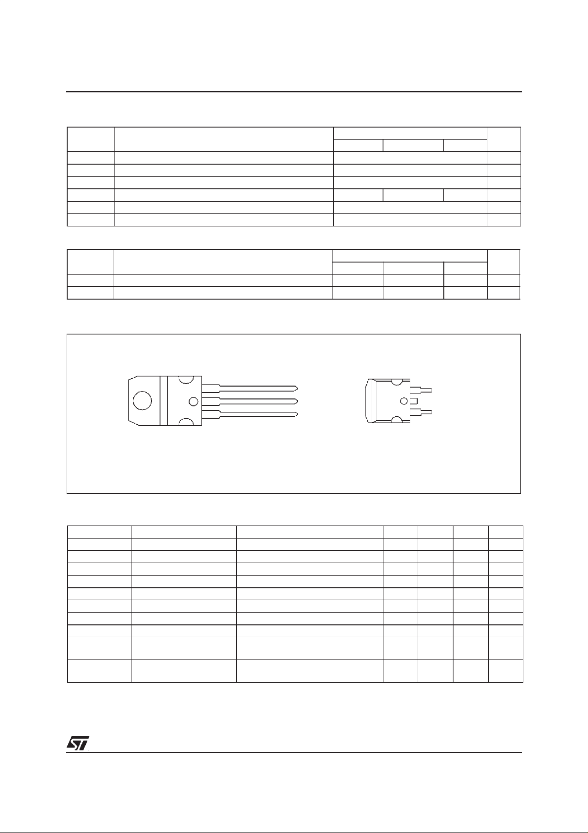
TO-220
ISOWATT220
3
1
D2PAK
ORDER CODES :
TO-220
VB408
ISOWATT220 VB408FI
D2PAK
start-up circuits, pneumatic valve drivers and current
sources. The device is able to drive resistive or inductive
loads with an output voltage from 1.25V to V
providing an internally limited output current; it has built in
short circuit and thermal shutdown protections. The
device does not provide galvanic insulation from main.
VB408B
1
3
2
IN-30V
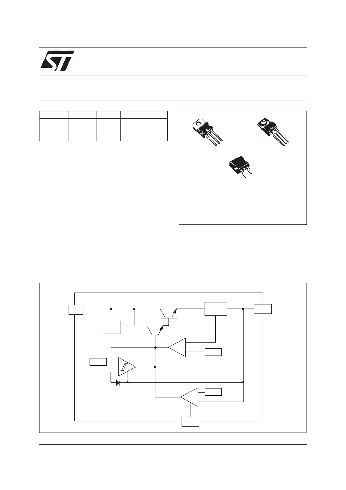
BLOCK DIAGRAM
+
_
CURRENT
SENSE
REF 2
REF 1
IN
V
Power
Stage
Current
Limitation
+
_
Thermal
Protection
Control
Signal
ADJ
REF 3
BIAS
CIRCUIT
+
_
September 1999 1/8
VOUT
FC00410
1
ABSOLUTE MAXIMUM RATING
Symbol Parameter
V
∆
IN,OUT
I
OUT
V
ESD
P
T
T
STG
Input to Output Voltage at 20 mA - 0.2 to 420 V
Output current Internally limited mA
Electrostatic discharge (R=1.5kΩ, C=100pF) 2000 V
Power dissipation at TC=25oC893189W
tot
Junction operating temperature - 40 to150 °C
j
Storage temperature - 55 to 150 °C
THERMAL DATA
Symbol Parameter
R
thj-case
R
thj-amb
(*) When mounted using the minimum recommended pad size on FR-4 board (1 inch2)
Thermal resistance junction-case (MAX) 1.4 4 1.4 °C/W
Thermal resistance junction-ambient (MAX) 60 60 35 (*) °C/W
CONNECTION DIAGRAM (TOP VIEW)
VB408 / VB408B / VB408FI
Value
TO-220 ISOWATT220 D2PAK
Value
TO-220 ISOWATT220 D2PAK
Unit
Unit
3
2
1
V
OUT
V
IN
ADJ
3
V
2
1
OUT
V
IN
ADJ
TO-220 / ISOWATT220 D2PAK
ELECTRICAL CHARACTERISTICS (VIN=300VDC; -25°C<Tj<125°C; I
specified)
LOAD
=15mA; V
=0V unless otherwise
ADJ
Symbol Parameter Test Conditions Min Typ Max Unit
Input Voltage 30 400 V
Input to Output Voltage 30 V
Output Reference Voltage V
Line Regulation V
IN
Load Regulation V
LOAD
=0V 1.20 1.24 1.28 V
ADJ
=0V; VIN=30 to 400 VDC 100 µV/V
ADJ
ADJ
=0V; I
=1 to 20 mA 6 mV/mA
LOAD
Adjustment Pin Current 50 70 90 µA
Minimum Load Current 1.2 mA
Output Current Limit 40 60 mA
Junction Temperature
Shutdown Limit
Junction Temperature
Shutdown Hysteresis
135 150 °C
25 °C
∆V
∆V
V
V
IN-VOUT
V
REF
OUT
/∆I
OUT
I
ADJ
I
BIAS
I
LIM
T
jsh
∆T
IN
/∆V
jsh
2/8
1
VB408 / VB408B / VB408FI
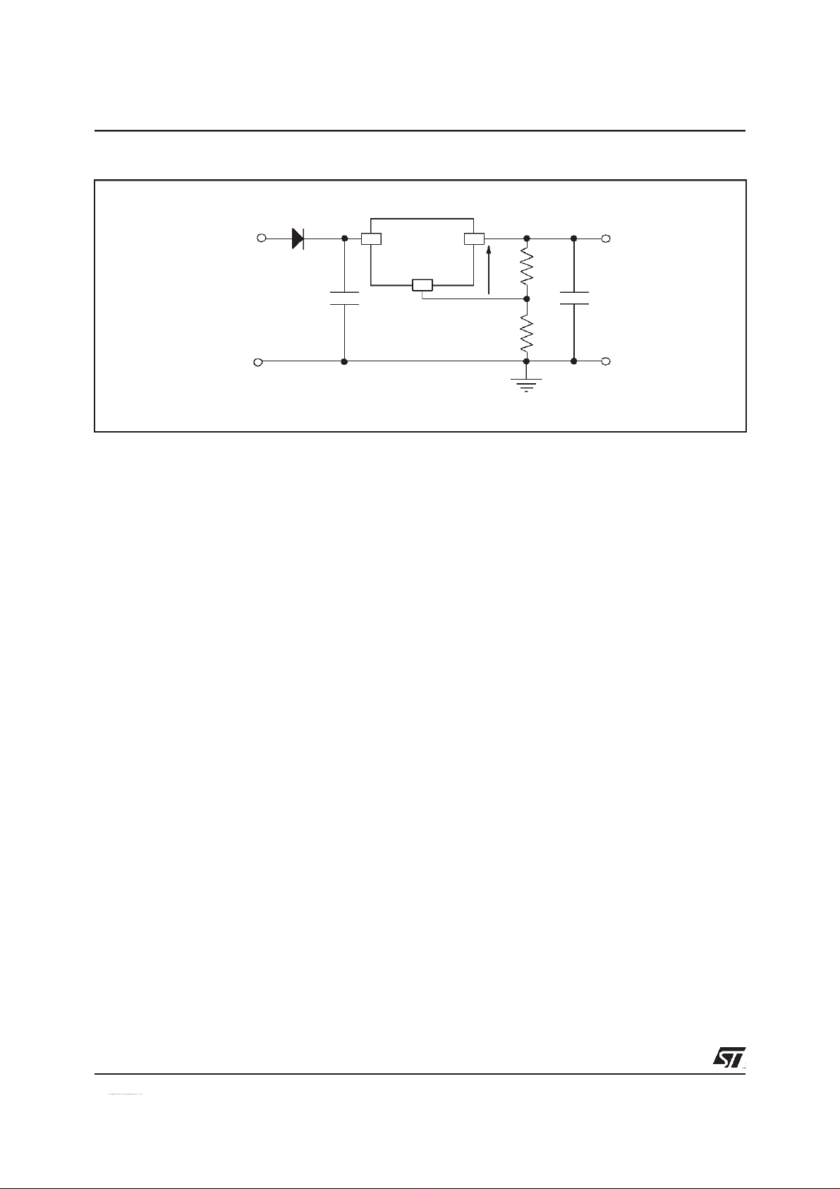
Figure 1: Typical application diagram
VIN
C1
VOUTVIN
VB408
A
DJ
VREF
R1
R2
V
OUT
C2
FC00420
OPERATION DESCRIPTION
The VB408, VB408B, VB408FI are positive voltage
regulators continuously adjustable from 1.25V to the input
voltage minus a dropout of 30V through an external
divider. In order to set the proper internal reference
voltage, a typical 70µA current has to be drawn from the
ADJ pin. Considering that, it results:
V
OUT =VREF
To simplify this formula, neglecting I
the term
V
REF/R1
R1must be chosen so toobtain a minimum 1.2mA current
flowing through the divider. In such a way the V
will be affected by an error <5%. The current set resistor
R
should be tied directly to the output terminal of the
1
regulator rather than near the load. This eliminates line
drops from appearing in series with the reference and
degrading regulation. The output voltage can also be set
by a zener diode put between the adjustment pin and
ground (Figure 2). The biasing current of the zener is
properly chosen by R
the ripple rejection and reduces the value of the worst
case output voltage error. In this case the output voltage
is given by:
V
OUT=VREF+VZ
In order to reduce excessive output ringing, a minimum
output capacitor C
will improve loop stability and output impedance. The
VB408/VB408B/VB408FI can be connected both to a DC
source or to a 285V r.m.s. line by a rectifier diode that
prevents a negative voltage to beapplied to thedevice. In
the first case the input capacitor C
whereas in the second case a high value of C
must be chosen. In fact, in this kind of application, C
to supply to the input pin the minimum allowed voltage
(1+R2/R1)+I
2
ADJR2
ADJ
resistor. The zener diode improves
1
of 0.1µF is suggested. This capacitor
1
with respect to
value
OUT
is not needed,
(> 1µF)
1
has
1
during the negative half wave. Obviously bigger C
more constant the input voltage is and consequently
smaller the output voltage ripple. For the right choice of
the input capacitor, you have also to remember that
increasing its value you will obtain an increased power
dissipation, and a heatsink could be required. The right
heatsink is determined by the load current, input voltage
and ambient temperature. In case of pulse or A.C.
operation the junction temperature is limited by the
thermal capacitances since the package and the heatsink
masses are able to absorb heat. If the junction
temperature reaches the thermal shutdown limit the
output stage of the regulator is turned-off so that only the
biasing current of the device can flow into the input pin.
Thermal hysteresis is added just to prevent oscillations.
The device is able to provide minimum 40 mA for a time
that is function of dissipated power and consequently of
the usedheatsink. In general the device is also suitable in
electronically switched motor housekeeping supply,
consumer equipments controls power supply or constant
current source.
APPLICATION EXAMPLE
The most common application for the device is in the DC/
DC converters with an input voltage up to 400 VDC and a
C
suggested value of 0,1µF.
2
Using an external rectifier an AC/DC converter can be
easily implemented, in this case the device can operate
with an AC voltage up to 285VRMS. In this case must be
used a minimum 1µF input capacitor to provide the load
current during the negative half cycle of the main. Another
important circuit that can be implemented is the start up
function for low voltage input PWM ICs directly from a
high voltage source (see figure 3).
value,
1
3/8
1

Figure 2: Regulation with Zener
VB408 / VB408B / VB408FI
VIN Vout
V
C1
IN
VB408
DJ
A
OUT
V
R1
Z1
Figure 3: Start-up circuit
V
IN
VOUTVIN
VB408
A
DJ
R1
C1
R2
C2
FC00430
C2
PWM
V
OUT
FC00470
4/8

VB408 / VB408B / VB408FI
TO-220 MECHANICAL DATA
DIM.
MIN. TYP MAX. MIN. TYP. MAX.
A 4.40 4.60 0.173 0.181
C 1.23 1.32 0.048 0.051
D 2.40 2.72 0.094 0.107
D1 1.27 0.050
E 0.49 0.70 0.019 0.027
F 0.61 0.88 0.024 0.034
F1 1.14 1.70 0.044 0.067
F2 1.14 1.70 0.044 0.067
G 4.95 5.15 0.194 0.203
H2 10.0 10.40 0.393 0.409
L2 16.4 0.645
L4 13.0 14.0 0.511 0.551
L5 2.65 2.95 0.104 0.116
L6 15.25 15.75 0.600 0.620
L7 6.2 6.6 0.244 0.260
mm. inch
L9 3.5 3.93 0.137 0.154
DIA. 3.75 3.85 0.147 0.151
5/8
1
11111
1
1

VB408 / VB408B / VB408FI
ISOWATT220 MECHANICAL DATA
DIM.
A 4.4 4.6 0.173 0.181
B 2.5 2.7 0.098 0.106
D 2.5 2.75 0.098 0.108
E 0.4 0.7 0.015 0.027
F 0.75 1 0.030 0.039
F1 1.15 1.7 0.045 0.067
F2 1.15 1.7 0.045 0.067
G 4.95 5.2 0.195 0.204
G1 2.4 2.7 0.094 0.106
H 10 10.4 0.393 0.409
L2 16 0.630
L3 28.6 30.6 1.126 1.204
L4 9.8 10.6 0.385 0.417
L6 15.9 16.4 0.626 0.645
L7 9 9.3 0.354 0.366
MIN. TYP MAX. MIN. TYP. MAX.
3 3.2 0.118 0.126
mm. inch
E
6/8
A
D
B
L3
L6
L7
¯
H
L2
F1
F
G1
G
F2
123
L4
1

D2PAK MECHANICAL DATA
VB408 / VB408B / VB408FI
DIM.
MIN. TYP MAX. MIN. TYP. MAX.
A 4.30 4.60 0.169 0.181
A1 2.49 2.69 0.098 0.106
B 0.70 0.93 0.027 0.036
B2 1.25 1.4 0.049 0.055
C 0.45 0.6 0.017 0.023
C2 1.21 1.36 0.047 0.053
D 8.95 9.35 0.352 0.368
E 10 10.28 0.393 0.404
G 4.88 5.28 0.192 0.208
L 15 15.85 0.590 0.625
L2 1.27 1.4 0.050 0.055
L3 1.4 1.75 0.055 0.068
mm. inch
D
A
C2
DETAIL”A”
C
A2
DETAIL”A”
A1
B2
E
L2
L
L3
B
G
7/8

VB408 / VB408B / VB408FI
Information furnished is believed to be accurate and reliable. However, STMicroelectronics assumes no responsibility for the consequences
of use of such information nor for any infringement of patents or other rights of third parties which may results from its use. No license is
granted by implication or otherwise under any patent or patent rights of STMicroelectronics. Specifications mentioned in this publication are
subject to change without notice. This publication supersedes and replaces all information previously supplied. STMicroelectronics products
are not authorized for use as critical components in life support devices or systems without express written approval of STMicroelectronics.
Australia - Brazil -Canada - China - France - Germany - Italy - Japan - Korea - Malaysia - Malta - Mexico - Morocco -
The Netherlands- Singapore - Spain - Sweden - Switzerland - Taiwan- Thailand - United Kingdom - U.S.A.
The ST logo is a registered trademark of STMicroelectronics
1999 STMicroelectronics - Printed in ITALY-All Rights Reserved.
STMicroelectronics GROUP OF COMPANIES
http://www.st.com
8/8
1
 Loading...