

HIGH VOLTAGE IGNITION COIL DRIVER
TYPE V
VB125SP 370 V 9 A 200 mA
■ PRIMARY COILVOLTAGE INTERNALLY SET
■ COIL CURRENT LIMIT INTERNALLY SET
■ LOGIC LEVEL COMPATIBLEINPUT
■ BATTERY OPERATION
■ SINGLE FLAG-ON COIL CURRENT
■ TEMPERATURE COMPENSATED HIGH
CL
VOLTAGE CLAMP
DESCRIPTION
The VB125SP is a high voltage power integrated
circuit made using SGS-THOMSON
Microelectronics Vertical Intelligent Power
Technology, with vertical current flow power
darlington and logic level compatible driving
circuit.
The VB125SP can be directly biased by using the
12V battery voltage, thus avoiding to use a low
voltage regulator. It has built-in protection circuits
for coil current limiting and collector voltage
clamping. It issuitable as smart, high voltage, high
current interface in advanced electronic ignition
system.
I
CL
I
CC
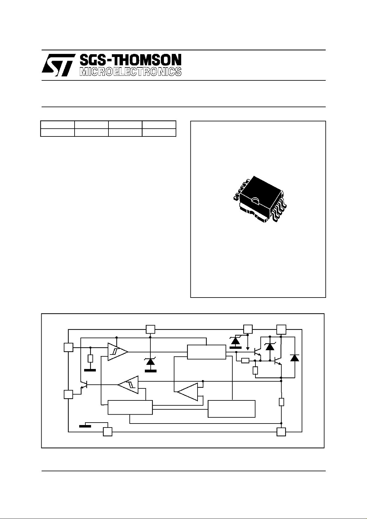
VB125SP
POWER IC
TARGET DATA
10
1
PowerSO-10
BLOCK DIAGRAM
C
S
8
HV
TAB
C
INPUT
V
CC
6
9
DRIVER
FLAG
FLAG
(*)
September 1997 1/8
Thisispreliminary information onanew product indevelopmentorundergoing evaluation. Details are subject to change without notice.
Pins 1...5
10
VOLTAGE
REFERENCE
7
GND (Control)
THERMAL
PROTECTION
R
SENSE
*
GND (Power)
1
VB125SP
ABSOLUTE MAXIMUM RATING
Symbol Parameter Value Unit
HV
C
I
C
V
CC
I
CC
I
S
V
IN
P
TOT
V
ESD
V
ESD
T
j
T
STG
THERMAL DATA
R
thj-case
R
thj-amb
CONNECTION DIAGRAM
Collector Voltage (Internally Limited) -0.3V to V
Collector Current (Internally Limited) 10 A
Driving Stage Supply Voltage -0.2 to 40 V
Driving Circuitry Supply Current 400 mA
Logic Circuitry Supply Ccurrent 100 mA
Input Voltage -0.3 to 6 V
Power Dissipation TBD W
ESD Voltage (HVC Pin) -4 to 4 KV
ESD Voltage (Other Pin) -2 to 2 KV
Operating Junction Temperature -40 to 150 °C
Storage Temperature Range -55 to 150 °C
Thermal Resistance Junction - Case MAX 1.2 °C/W
Thermal Resistance Junction - Ambient MAX 62.5 °C/ W
CLAMP
V
V
CC
GND
Cs
INPUT
FLAG
PIN FUNCTION
No Name FUNCTION
1-5 GND Emitter Power Ground
6V
7 GND Control Ground (*)
8C
9 INPUT Logic Input Channel
10 FLAG Diagnostic Output Signal
TAB HVC Primary Coil Output Driver
(*) Pin 6 must be connected to pins 1-5externally
6
10
CC
S
HVC
5
GND
GND
GND
GND
1
Logic Supply Voltage
Logic Level Supply Voltage Filter Capacitor
GND
2/8
1

VB125SP
ELECTRICAL CHARACTERISTICS (V
to
6mH; unless otherwise specified; See Note 1)
= 6 to 24V; -40°C<Tj<125°C; R
bat
= 400 to 700m ; L
coil
Ω
Symbol Parameter Test Conditions Min. Typ. Max. Unit
V
CL
V
CE(sat)
I
CC(off)
I
CC(on)
I
CL
V
inH
V
inL
V
IN(hyst.)
I
inH
I
inL
V
diagH
V
diagL
I
diagTH
I
diag
I
diag(leak)
V
F
E
s/b
T
t
d(on)
t
d(off)
t
d(off)
j
High Voltage Clamp IC= 6.5 A; (See Note 2) 340 370 400 V
Saturation Voltage of the Power
Stage
Power Off Supply Current
Power On Supply Current
I
= 5A; Vin= 4V (See Note 3) 2 V
C
=0.4V V
V
in
=0.4V V
V
in
=4V V
V
In
=4V V
V
in
= 14V(Notes 4-5)
bat
=24V
bat
<14V (Note 4-5)
bat
=24V
bat
20
80
220
300
Coil Current Limit Vin= 4 V (See Note 6-7) 8 10 A
High Level Input Voltage 4 V
Low Level Input Voltage 0.8 V
Input Hysteresis Voltage 0.4 V
High Level Input Current Vin= 4 V 10 150
Low Level Input Current Vin= 0.8 V -100
High Level Diagnostic Output
Voltage
Low Level Diagnostic Output
Voltage
Current Threshold Level Diagnostic
R
EXT
(See Note 8)
R
EXT
(See Note 8)
T
j
High Level Flag Output Current IC>I
=22K C
Ω
Ω
=22K C
=25°C (See Note 7and fig. 5) 4.25 4.5 4.75 A
(See Note 7) 0.5 mA
DiagTH
EXT
EXT
=1nF
=1nF
3.5 5.5 V
0.5 V
Leakage Current on Flag Output Vin=LOW 10 µA
Antipallel Diode Forward Voltage IC=-1A 2 V
Single Pulse Avalanche Energy 300 mJ
Thermal Output Current Control IN = ON (See Note 9) 150 °C
Turn-on Delay Time of Output
Current
Turn-off Delay Time of Output
Current
Turn-off Delay Time of Output
Current
(See Note 10) TBD µs
(See Note 11) TBD
(See Note 11) TBD µs
coil
=2
mA
mA
mA
mA
µA
µA
µs
FIGURE 1: Temperature Compensated High
FIGURE 2: Electrical Characteristic of the Circuit
Voltage Clamp Shown in Figure 1
[mA]
I
HVC
nV
Z
R
i1
KV
R
ii
be
R
sens
PWR GND
C
40
30
20
10
100 200 300 400
slope ∝ ∑Ri
nV
Z
V
[V]
V
CL
CE
3/8

VB125SP
NOTE 1 Parametric degradation are allowed with 6V < V
< 10V and V
bat
bat
> 24V.
NOTE 2 In the high voltage clamping structure of this device a temperature compensation has been implemented. The
circuit schematic is shown in fig. 1. The KVbe cell takes care of the temperature compensation. The whole
electrical characteristic of the new circuit is shown in fig. 2. Up to V
leakage current of the power stage); for nV
compensation circuit (typical slope
≅Ω Ω
20 K ) as soon as the Vcl is reached the dinamic resistance drop to
Z<VCE<VCL
a current begins to flow across the resistances of the KVbe
=nVZno current will flow into the collector (just the
CE
~4 to
protect the device against overvoltage (See Fig. 3).
NOTE 3 The saturation voltage of the Power stage includes the drop on the sensing resistor.
NOTE 4 Considering the different ways of operation of the device (with or without spark, etc...) there are some short
periods of time in which the output terminal (HV
inductances and stray capacitances of the ignition coil.With VIPower devices, if no corrective action is taken, these
) is pulled below ground by a negative current due to leakage
C
negative currents can cause parasitic glitches on the diagnostic output. To kill this potential problem, a circuit that avoids
the possibility for the HV
implemented in the VB125SP.For this reason there are some short periods in which a current exceeding 220 mA flows
in the pin V
.
D
NOTE 5 A zener protection of 16V (typical) is placed on the supply pin (V
For this reason, when the battery voltage exceedes that value, the current flowing into V
maximum current specified at V
resistor.
to be pulled undeground, by sending the required negative current from the battery is
C
) of the chip to protect the internal circuitry.
CC
=14V (both in power on and power off condictions) : it will be limited by an internal
bat
cc pin can be greater than the
NOTE 6 The primary coil current value Icl must be measured 1 ms after desaturation of the power stage.
NOTE 7 These limits apply with regard to the minimum battery voltage and resistive drop on the coil and cables that permit
to reach the limitation or diagnostic level.
NOTE 8 No internal Pull-Down.
NOTE 9 Tj
min= 150 °C means that the behaviour of the device will not be affected for junction temperature lower than
150°C.For higher temperature, the thermal protection circuit will begin its action reducing the Icl limit according with the
power dissipation. Chip temperature is a function of the Rth of the whole system in which the device will be operating
(See Fig.4).
NOTE 10 Propagation Time measured from input voltage rising edge to 50% of output voltage falling edge.
NOTE 11 As soon as the input signal is switched low the stored charges in the base of the power transistor are removed
and the so called «Turn-off Delay Time of Coil Current» begins; after at the «Turn-off Fall Time of Coil Current» starts
and, at the same time, the HVC rises.
dLH is defined as the time between the negative edge of the input pulse to the point where the HVC reaches 100V.
t
t
fLH is defined as the delay between the 90% and the 10% of the coil current.
4/8

FIGURE 3: Vcl with load L ≅ 4mH
VB125SP
FIGURE 4: Output Current Waveform after Thermal Protection Activation.
5/8
1

VB125SP
FIGURE 5: Waveforms
INPUT
IC
HVC
FLAG
FIGURE 7: Application Circuit
4.5A
6.5A
FIGURE 6: Flag Current Versus Temperature
I
(A)
flag
5.0
4.5
4.0
3.5
-50
0
50
100
T
case
(oC)
µP
1nF 22K
C
EXT
R
EXT
INPUT
FLAG
V
CC
VB125SP
GND
HVC
PWR
GND
100nF
C
V
BAT
S
6/8
1

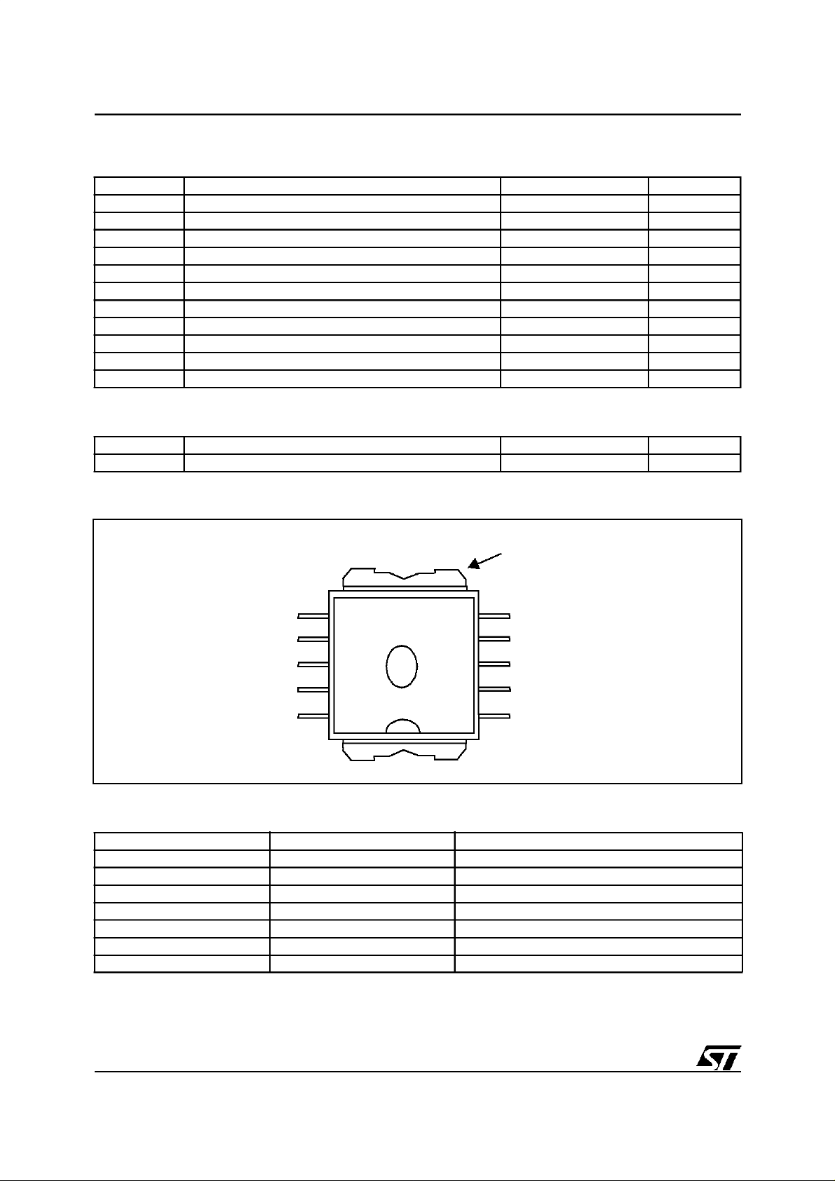
PowerSO-10 MECHANICAL DATA
VB125SP
DIM.
MIN. TYP. MAX. MIN. TYP. MAX.
mm inch
A 3.35 3.65 0.132 0.144
A1 0.00 0.10 0.000 0.004
B 0.40 0.60 0.016 0.024
c 0.35 0.55 0.013 0.022
D 9.40 9.60 0.370 0.378
D1 7.40 7.60 0.291 0.300
E 9.30 9.50 0.366 0.374
E1 7.20 7.40 0.283 0.291
E2 7.20 7.60 0.283 0.300
E3 6.10 6.35 0.240 0.250
E4 5.90 6.10 0.232 0.240
e 1.27 0.050
F 1.25 1.35 0.049 0.053
H 13.80 14.40 0.543 0.567
h 0.50 0.002
L 1.20 1.80 0.047 0.071
q 1.70 0.067
B
==
==
HE
h
A
F
A1
610
51
eB
M
0.25
D
==
D1
==
E2
==
DETAIL”A”
DETAIL”A”
Q
0.10 A
E1E3
==
SEATING
PLANE
A
C
α
B
E4
==
SEATING
PLANE
A1
L
==
0068039-C
7/8

VB125SP
Information furnished is believed to be accurate and reliable. However, SGS-THOMSON Microelectronics assumes no responsability for
the consequences of use of such information nor for any infringement of patents or other rights of third parties which may results from its
use. No license is granted by implication or otherwise under any patent or patent rightsof SGS-THOMSON Microelectronics. Specifications
mentioned in this publication are subject to change without notice. This publication supersedes and replaces all information
previously supplied. SGS-THOMSON Microelectronics products are not authorized for use as critical components in life support devices or
systems without express written approval of SGS-THOMSON Microelectronics.
1997 SGS-THOMSON Microelectronics - Printed in Italy - All Rights Reserved.
Australia - Brazil - France - Germany - Hong Kong - Italy - Japan - Korea - Malaysia - Malta - Morocco - The Netherlands - Singapore -
SGS-THOMSON Microelectronics GROUP OF COMPANIES
Spain - Sweden - Switzerland - Taiwan- Thailand - United Kingdom - U.S.A.
8/8
 Loading...