

VB026SP
HIGH VOLTAGE IGNITION COIL DRIVER
POWER IC
TYPE V
VB026S P 360 V 9 A 100 mA
■ PRIMARYCOIL VOLTAGEINTERNALLY SET
■ COIL CURRENT LIMIT INTERNALLYSET
■ LOGICLEVEL COMPATIBLE INPUT
■ DRIVINGCURRENT QUASI
cl
I
cl
I
d
PROPORTIONALTO COLLECTOR
CURRENT
■ SINGLE FLAG-ONCOILCURRENT
DESCRIPTION
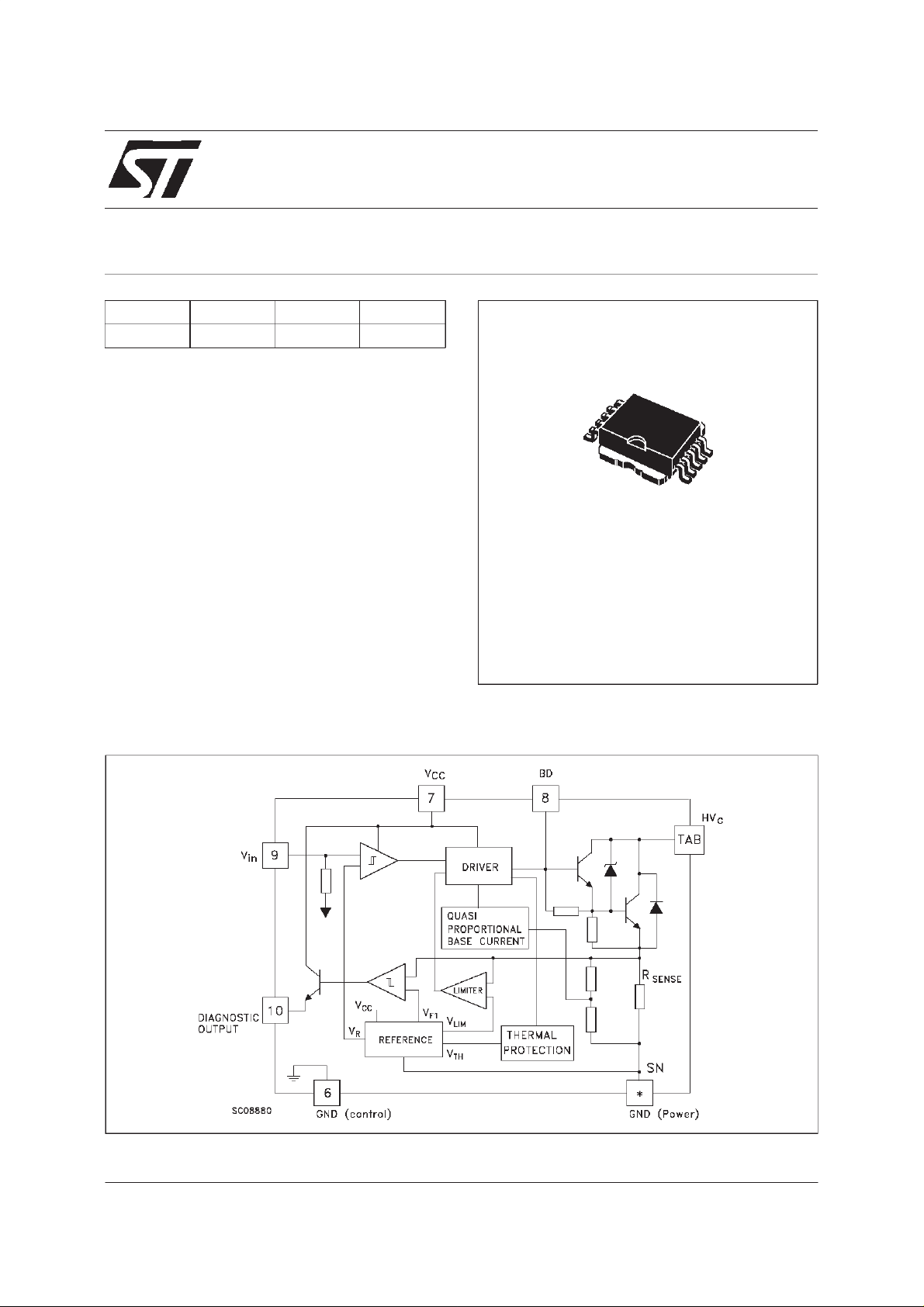
The VB026SP is a high voltage power integrated
circuit made using STMicroelectronics VIPower
Technology, with vertical current flow power
darlingtonandlogiclevelcompatibledrivingcircuit.
Built-in protection circuits for coil current limiting
and collector voltage clamping allows the
VB026SP to be used as a smart, high voltage,
high current interface in advanced electronic
ignition systems.
BLOCK DIAGRAM
10
1
PowerSO-10
March 1999
1/7
VB026SP
ABSOLUTEMAXIMUMRATING
Symbol Para met e r Val u e Uni t
HV
I
I
C(gnd)
V
I
I
s(gnd)
V
I
f
V
out(flag)
I
out(flag)
I
BD
V
P
max
E
V
ESD
V
ESD
T
T
(*) With 10 mils Al wire
Collec t or Voltage ( I nternally Limi t ed ) -0. 3 t o V
C
Collec t or Current (I n t ernally Li m ited) 10 A
C
clamp
DC C ur rent on Emitter Powe r ± 10.5 (*) A
Driving Stage Supply V oltage -0.3 to 7 V
CC
Driving C ir c uit r y Supply Current ± 200 mA
s
DC C ur rent on Groun d P in ± 1A
Input Voltage -0. 3 t o VCC+0.3 V
in
Maximum I nput C urrent 100 mA
in
Logic In put Fr eque nc y in O perative Mode DC to 150 Hz
in
Out put Volta ge Prima r y T h r es hold Current Level -0. 3 t o VCC+0.3 V
Flag Out put Cu rr ent 100 m A
Input Darlington Bas e C urrent 150 m A
Input Darlington Bas e V oltage Int er na lly Limit ed V
BD
Power Dissi pation (TC= 105oC) TB D W
Clampe d Ene r gy D ur in g Out put Power Clampin g 300 mJ
s/b
ESD Voltage (HVC Pin) ± 4KV
ESD Voltage (O ther Pins) ± 2KV
Oper ating Junction Temperat ure -40 to 150
j
St orage Temperatur e Range -55 to 150
stg
V
o
C
o
C
THERMALDATA
R
thj-case
R
thj-h
T
sold
(*) see application noteAN515 on VIPower databook 1stedition
Ther mal Res is t an ce Junction Case (MAX ) 1.2
Ther mal Res is t an ce Junction Heats i nk wit h FR4 (MA X) TBD (*)
Lead Tempera tur e Durin g Soldering (MA X) TB D (*)
o
C/W
o
C/W
o
C
2/7
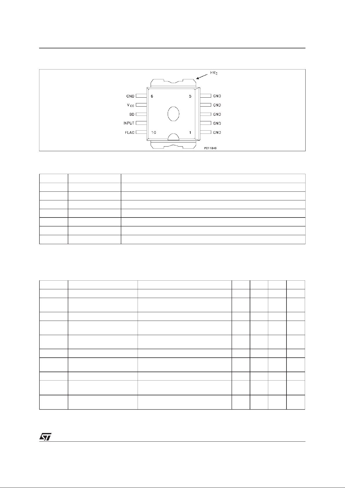
CONNECTIONDIAGRAM
PIN FUNCTION
No NAME FUNCTION
1-5 GND Emitter Po wer G r ound
6 G ND Control Ground (*)
7V
CC
8 BD Base Da rl ington
9 I NP U T Logi c Inp ut Channel (I nternal P ul l- do wn)
10 FLAG Diagnost ic O u t pu t Signa l (Op en E m it t e r)
TAB HVC Primary Coil Output Driv er (Ope n Coll ector)
(*) Pin 6 must beconnected to pins1-5 externally
Logic Supply Voltage
VB026SP
ELECTRICAL CHARACTERISTICS (5.3V < Vb< 24V;VCC=5V±10%;-40oC<Tj<125oC;
R
=580 mΩ;L
coil
Symbol Parameter Test Cond itions Min. Typ. Max. Unit
V
V
ce(sat)
High V oltage C lam p I
cl
Saturation Voltage of The
Power Stage
I
d(stdby)
I
CC
I
CC(peak)
Stand -by Sup ply Current IN = OFF 10 mA
DC L ogic Current Vb=16V Ic=6.5A f=100Hz
Peak DC Lo gic Current
During On Phase
V
I
I
c( le ak)
I
C(in fl)
DC Logic Voltage 4.5 5.5 V
CC
Coil Cur rent Limi t -40oC<Tj<125oC
cl
Outp ut l eak age C ur rent IN = OFF V
Collect or Current with
Float ing Input
T
shdw
Therm al Tem peratu r e
Outp ut C urrent Control
= 3.75 mH; unless otherwisespecified; seenote 1)
coil
= 6.5 A 320 360 420 V
coil
Ic=6.5A; Vin=4V 1.5 2 V
Load = C oil V
CC
=5.5V
Ic= 6. 5 A (se e f i gur e 1) 100 150 mA
(see not e 2 and figure 1)
= 24V 0.8 mA
HVC
VCC = 5 V VB at = 13. 5 V
=1KΩ; Inp ut F loati ng
R
LOAD
OUT = O N (see figure 2 ) 150 (*)
40 mA
8.25 10 A
0.8 mA
o
C
3/7

VB026SP
ELECTRICAL CHARACTERISTICS (continued)
Symbol Parameter Test Cond itions Min. Typ. Max. Unit
V
V
V
in(hys)
I
inH
I
inL
I
inpd
V
diagH
V
diagL
I
diagTH
I
diagTD
I
diag
I
diag(leak)
V
E
t
pHL
t
pLH
Note 1: Parametricdegradation are allowed with 5.3 < Vb< 10V and Vb> 24V.
Note 2: Theprimary coil current value I
Note 3: No Internal Pull-Down
(*) Internally limited
High Lev e l Input V olt a ge VCC=4.5V 4 V
inH
Low Lev e l Input Vol t ag e VCC=5.5V -0.3 0.8 V
inL
Input Thr esho ld
0.4 V
Hysteresis
High Lev e l Input Cur rent Vin= 4 V 100 µA
Low Lev e l Input Curr ent Vin=0.8V -100 µA
Input Act ive Pull- D own Vin= 4 V 10 100 µA
High Lev e l Flag Out put
Voltage
Low Lev e l Flag Outp ut
Voltage
Coil Cur rent Leve l
=22KΩ C
R
EXT
EXT
=1nF
(see not e 3)
=22KΩ C
R
EXT
EXT
=1nF
(see not e 3)
Tj=25oC (see figure 1) 6.15 6.5 6.8 5 A
V
-1 V
CC
Threshold
Coil Cur rent Leve l
(see figure 3)
Threshold Drift
High Lev e l Flag Out put
IC>I
diagTHVdiag
=3V 0.5 TBD mA
Current
Leakage Cu rrent O n Fla g
Vin=LOW VCC= 5.5V 10 µA
Output
Antiparallel Diode
F
Ic=-1A 2 V
Forward Voltage
Single Pulse Avalanche
s/b
Energy
Turn-o n Delay Tim e of
Coil Curre nt
Turn-off Delay Tim e of
Coil Curre nt
must bemeasured 1ms after desaturation of the power stage.
cl
IC=8A LC=6mH
(see figure 4)
=0.5Ω Lc=3.75mH
R
c
(see figure 5)
=0.5Ω Lc=3.75mH Ic=6.5A
R
c
(see figure 5)
180 mJ
TBD µs
TBD µs
CC
CC
0.5 V
V
V
PRINCIPLEOF OPERATION
The VB026SP is mainly intended as a high
voltage power switch device driven by a logic
levelinput and interfaces directly to a high energy
electronicignitioncoil.
The input Vin of the VB026SP is fed from a low
power signal generated by an external controller
that determinesboth dwelltime and ignition point.
During Vin high (≥ 4V) the VB026SP increases
current in the coil to the desired, internally set
currentlevel.
After reaching this level, the coil current remains
constant until the ignition point, that corresponds
to the transition of Vin from high to low (typ. 1.9V
threshold).
During the coil current switch-off, the primary
4/7
voltage HVc is clampedat an internally set value
Vcl, typically360V.
The transitionfrom saturation to desaturation,coil
current limiting phase, must have the ability to
accomodate an overvoltage. A maximum
overshootof 20V is allowed.
FEEDBACK
When the collector current exceeds 6.5A, the
feedback signal is turned high and it remains so,
untilthe input voltage isturned-off.
OVERVOLTAGE
The VB026SP can withstand the following
transientsof the battery line:
-100V/2msec(R
+100V/0.2msec(R
+50V/400msec(R
=10Ω)
i
=10Ω)
i
=4.2 Ω, with VIN=3V)
i

VB026SP
Fig. 1 Main WaveformsDuring On Phase Fig. 2 Output Current WaveformAfter Thermal
ProtectionActivation
FIG.4 Single PulseTypicalEs/b CurveFig. 3 FlagCurrent Versus Temperature
FIG. 5 PropagationTimes Definitions.
200 V
50 %
10 %
tt
pHL pLH
HVC
INPUT
10 %
SC10930
5/7

VB026SP
PowerSO-10MECHANICAL DATA
DIM.
mm inch
MIN. TYP. MAX. MIN. TYP. MAX.
A 3.35 3.65 0.132 0.144
A1 0.00 0.10 0.000 0.004
B 0.40 0.60 0.016 0.024
c 0.35 0.55 0.013 0.022
D 9.40 9.60 0.370 0.378
D1 7.40 7.60 0.291 0.300
E 9.30 9.50 0.366 0.374
E1 7.20 7.40 0.283 0.291
E2 7.20 7.60 0.283 0.300
E3 6.10 6.35 0.240 0.250
E4 5.90 6.10 0.232 0.240
e 1.27 0.050
F 1.25 1.35 0.049 0.053
H 13.80 14.40 0.543 0.567
h 0.50 0.002
L 1.20 1.80 0.047 0.071
q 1.70 0.067
α 0
o
o
8
==
==
HE
h
A
F
A1
610
51
eB
M
0.25
D
==
D1
==
DETAIL”A”
E2
==
DETAIL”A”
Q
B
0.10 A
E1E3
==
SEATING
PLANE
A
C
α
B
E4
==
SEATING
PLANE
A1
L
==
0068039-C
6/7

VB026SP
Information furnished isbelieved tobeaccurate and reliable. However, STMicroelectronics assumes noresponsibility for the consequences
of use of such information nor for any infringement of patents or other rights of third parties which may result from its use. No license is
granted by implication or otherwise under any patent or patentrights of STMicroelectronics. Specification mentioned inthis publication are
subject tochange without notice. Thispublication supersedes and replaces allinformation previously supplied. STMicroelectronics products
are notauthorized for use as critical components in life support devices or systems without express written approval of STMicroelectronics.
The STlogo is atrademark of STMicroelectronics
1999 STMicroelectronics – Printedin Italy – AllRights Reserved
STMicroelectronicsGROUP OF COMPANIES
Australia - Brazil -Canada - China -France -Germany - Italy- Japan - Korea - Malaysia - Malta -Mexico - Morocco - The Netherlands-
Singapore -Spain - Sweden -Switzerland - Taiwan -Thailand - UnitedKingdom - U.S.A.
http://www.st.com
.
7/7
 Loading...