

®
EMI FILTER AND LINE TERMINATION
A.S.D.
APPLICATIONS
EMI Filter and line termination for USB downstream ports on:
- Desktop computer
- Notebooks
- Workstations
- USB Hubs
FEATURES
Monolithic device with recommended line termi-
n
nation for USB downstream ports
Integrated Rt series termination and Ct bypass-
n
ing capacitors.
Integrated ESD protection
n
Small package size
n
DESCRIPTION
The USB specification requires USB
downstream ports to be terminated with
pull-down resistors fromthe D+ and D- lines to
ground. On the implementation of USB
systems, the radiated and conducted EMI
should be kept within the required levels as
stated by the FCC regulations. In addition to
the requirements of termination and EMC
compatibility, the computing devices are
required to be tested for ESD susceptibility.
The USBDFxxW5 provides therecommended line
termination while implementing a low pass filter to
limit EMI levels and providing ESD protection
which exceeds IEC 61000-4-2 level 4 standard.
The device is packaged in a SOT323-5L which is
the smallest available lead frame package (50%
smaller than the standard SOT23).
BENEFITS
n
EMI / RFI noise suppression
n
Required line termination for USB downstream
ports
n
ESDprotectionexceeding IEC61000-4-2 level4
n
High flexibility in the design of high density
boards
n
Tailored to meet USB 1.1 standard
FOR USB DOWNSTREAM PORTS
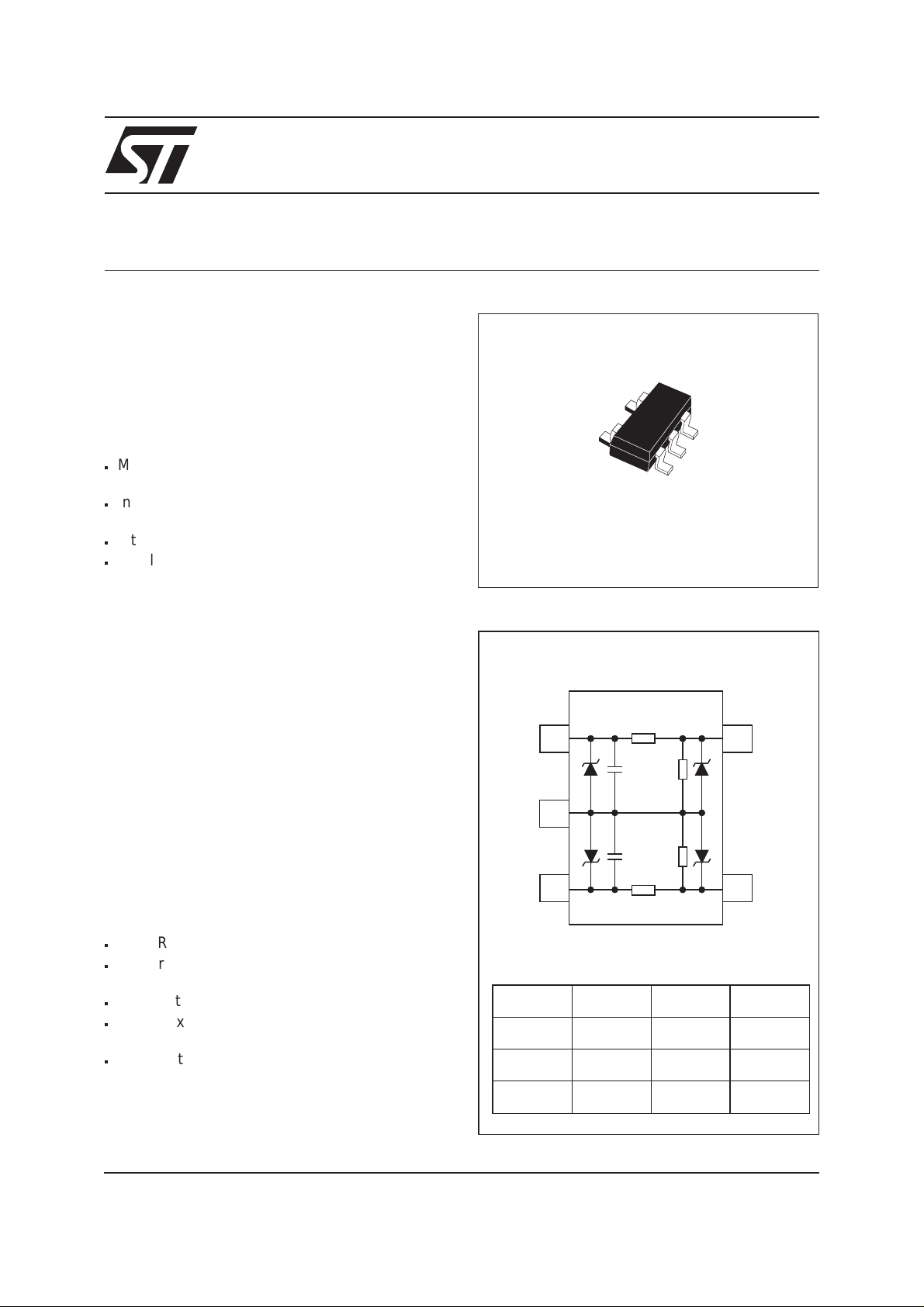
USBDFxxW5
SOT323-5L
FUNCTIONAL DIAGRAM
D+ In
Gnd
D- In
Code 01 33Ω 15kΩ 47pF
Code 02 15Ω 15kΩ 47pF
Rt
Ct
Rd
Rd
Ct
Rt
Rt Rd Ct
D+ Out
D- Out
TM: ASDandTRANSIL are a trademarks of STMicroelectronics.
May 2000 Ed : 1C
Tolerance ±10% ±10% ±20%
1/9

USBDFxxW5
COMPLIES WITH THE FOLLOWING ESD
STANDARDS:
IEC-61000-4-2, level 4
±15 kV (air discharge)
±8 kV (contact discharge)
MIL STD 883C, Method 3015-6
Class 3 C = 100 pF R = 1500 Ω
3positivestrikes and 3negative strikes (F=1Hz)
ABSOLUTE MAXIMUM RATINGS (T
amb
= 25°C)
Symbol Parameter Value Unit
V
PP
ESD discharge IEC 61000-4-2, contact discharge
ESD discharge - MIL STD 883 - Method 3015-6
T
j
T
stg
T
L
T
op
P
r
Junction temperature
Storage temperature range
Lead solder temperature (10 second duration)
Operating temperature Range
Power rating per resistor
ELECTRICAL CHARACTERISTICS (T
amb
= 25°C)
±15
±25
150 °C
- 55 to +150 °C
260 °C
0to70 °C
100 mW
Symbol Parameters Testconditions Min Typ Max Unit
V
BR
V
F
Diode breakdown voltage IR= 1mA
Diode forward voltage drop IF= 50mA
6V
0.9 V
kV
kV
2/9
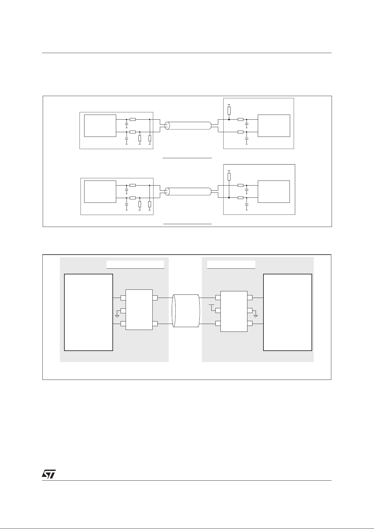
APPLICATION INFORMATION
Fig. A1: USB Standard requirements
Full-speed or
Low-speed USB
Transceiver
Host or
Hub port
Full-speed or
Low-speed USB
Transceiver
Host or
Hub port
Rt
Ct
Rt
15k
Ct
Rt
Ct
Rt
15k
Ct
15k
15k
D+
Twisted pair shielded
D-
D+
D-
Zo = 90ohms
5m max
FULL SPEED CONNECTION
Untwisted unshielded
3m max
LOW SPEED CONNECTION
D+
D-
D+
D-
+Vbus
1.5k
+Vbus
1.5k
Rt
Ct
Rt
Ct
Rt
Ct
Rt
Ct
Full-speed USB
Transceiver
Hub 0 or
Full-speed function
Low-speed USB
Transceiver
Hub 0 or
Low-speed function
USBDFxxW5
APPLICATION EXAMPLE
Host/Hub USB
port transceiver
USBDF
xxW5
Upstream portDownstream port
D+ (1)
CABLE
D+
D-
(1) for a low-speed port
(2) for a full-speed port
D- (2)
+Vbus
D- (1)
D+ (2)
USBUF
xxW6
Peripheral
transceiver
3/9

USBDFxxW5
EMI FILTERING
Current FCC regulations requires thatclassB computing devices meet specifiedmaximum levelsfor both
ratiated and conducted EMI.
- Radiated EMI covers the frequency range from 30MHz to 1GHz.
- Conducted EMI covers the 450kHz to 30MHz range.
For the types of devices utilizing the USB the most difficult testto pass is usually theradiated EMI test. For
this reason the USBDF device is aiming to minimize radiated EMI.
The differential signal (D+ and D-) of the USB does not contribute significantly to radiated or conducted
EMI because the magnetic field of the two conductors exactly cancels each other.
Theinsideof the PC environment isverynoisy and designers must minimisenoisecoupling from the different sources. D+ and D- must not be routed near highspeed lines (clocks...).
Induced common mode noise can be minimised by running pairs of USB signals parallel to each other and
runninggroundedguard trace oneach side ofthesignal pair fromtheUSB controller totheUSBDF device.
Ifpossible,locatetheUSBDF device physically near the USB connectors. Distance betweentheUSBcontroller and the USB connector must be minimized.
The 47pF (Ct) capacitors are used to bypass high frequency energy to ground and for edge control, and
must be placed between the USB Controller and the series termination resistors (Rt). Both Ct and Rt
should be placed as close to the USB Controller as practicable.
TheUSBDFxxW5ensure a filteringprotection against ElectroMagneticandRadioFrequency Interferences
thanks to its low-pass filter structure. This filter is characterized by the following parameters :
- cut-off frequency
- Insertion loss
- high frequency rejection
Fig. A3 shows the attenuation curve for frequencies up to 3GHz.
Fig. A2: Measurement configuration
TG OUT
50 Ω
Vg
TEST BOARD
UD1
RF IN
50 Ω
Fig. A3: USBDFxxW5 attenuation curve.
Insertion loss (dB)
0
-10
-20
-30
1 10 100 1000 3000
F (MHz)
ESD PROTECTION
Inadditiontotherequirements of termination and EMC compatibility, computing devices arerequiredtobe
tested for ESD susceptibility. This test is described inthe IEC 61000-4-2and is alreadyin place inEurope.
This test requires that a device tolerates ESD events and remainoperational without user intervention.
The USBDFxxW5 is particularly optimizedto perform ESD protection. ESDprotection is based on the use
of device which clamps at :
Vinput V R I
BR d PP
=+.
This protection function is splitted in 2 stages. As shown in figure A4, the ESD strikes are clamped by the
first stage S1 and then its remaining overvoltage is applied to the second stage through the resistor R.
Such a configuration makes the output voltage very low at the Vout level.
4/9

Fig. A4: USBDFxxW5 ESD clamping behavior
USBDFxxW5
V
PP
ESD Surge
Rg
S1
Rd
V
BR
Vinput
R
Voutput
USBDFxxW5
S2
Rd
V
Rload
BR
Device
to be
protected
To have a good approximation of the remaining voltages at both Vin and Vout stages, we give the typical
dynamical resistance value Rd. By taking into account these following hypothesis : Rt>Rd, Rg>Rd and
Rload>Rd, it gives these formulas:
RV RV
gBR dg
+..
R
g
R V R Vinput
tBR d
+..
R
t
Theresultsof the calculationdonefor V
Vinput
Voutput
=8kV,Rg=330Ω(IEC61000-4-2 standard), VBR=7V(typ.)
PP
=
=
and Rd = 1Ω (typ.) give:
Vinput = 31.2 V
Voutput = 7.95 V
This confirms the very lowremaining voltage across the device tobe protected. It is also importantto note
that in this approximation the parasitic inductance effect was not taken into account. This could be few
tenths of volts during few ns atthe Vinside. This parasiticeffect isnot presentat the Voutside duethe low
current involved after the resistance R.
The measurements done here after show very clearly (Fig. A6) the high efficiency of theESD protection :
- no influence of the parasitic inductances on Vout stage
- output clamping voltage very close to V
(positive strike) and -VF(negative strike)
BR
Fig. A5: Measurement board
ESD
SURGE
TEST BO ARD
16kV
Air
Discharge
Vin Vout
UD1
5/9

USBDFxxW5
Fig. A6: Remaining voltage at both stages S1 (Vinput) and S2 (Voutput) during ESD surge.
a. Positive surge
b.Negative surge
PleasenotethattheUSBDFxxW5 is not only acting for positive ESDsurgesbutalso for negative ones. For
these kinds of disturbances it clamps close to ground voltage as shown in Fig. A6b.
LATCH-UP PHENOMENA
The early ageing and destruction of IC’s is often due to latch-up phenomena which is mainly induced by
dV/dt. Thanks to its structure, the USBDFxxW5 provides a high immunity to latch-up phenomena by
smoothing very fast edges.
CROSSTALK BEHAVIOR
Fig. A7: Crosstalk phenomena
R
G1
V
G1
R
G2
V
G2
Line 1
Line 2
R
L1
R
L2
αβ
V+ V
1G1 12G2
V+ V
αβ
2G2 21G1
DRIVERS
Thecrosstalkphenomena is duetothe coupling between2 lines. Thecouplingfactor ( β
RECEIVERS
orβ21)increases
12
when the gap across lines decreases, this is the reason why we provide crosstalk measurements for
monolithic device to guarantee negligeable crosstalk between the lines. In the example above the expected signal on loadR
partofthe V
signalrepresentsthe effect ofthecrosstalk phenomenon oftheline 1 ontheline 2. Thisphe-
G1
is α2VG2, in fact thereal voltageat this point has gotan extra value β21VG1. This
L2
nomenon has to be taken intoaccount when thedrivers impose fast digital data or high frequency analog
signals in the disturbing line. The perturbed line will be more affected if it works with low voltagesignal or
high load impedance (few kΩ).
6/9

USBDFxxW5
Fig. A8: Analog Crosstalk measurements
Fig. A9: Typical Analog Crosstalk results
Analog crosstalk (dB)
0
-20
TG OUT
50 Ω
Vg
TEST BOARD
UD1
RF IN
50 Ω
-40
-60
-80
-100
1 10 100 1,000
frequency (MHz)
Figure A8givesthemeasurementcircuitfortheanalog crosstalk application. In figure A9, the curve shows
the effectoftheD+cellontheD- cell. In usual frequency range of analog signals (up to 100MHz) the effect
on disturbed line is less than -46dB.
Fig. A10: Digital crosstalk measurements configu-
Fig. A11: Digital crosstalk results
ration
+5V +5V
Square
Pulse
Generator
5KHz
+5V
74HC04
Line 1
V
G1
Line 2
USBDF
xxW5
74HC04
b
V
21
G1
Figure A10 showsthe measurement circuit used to quantify the crosstalk effect in a classical digital application.
Figure A11 shows that in such a condition signal from 0 to 5V and rise time of few ns, the impact on the
other line is less than 100mV peak to peak (Below the logic high voltage threshold).The measurements
performed with falling edges give the same results.
7/9

USBDFxxW5
TRANSITION TIMES
This lowpassfilterhasbeen designed in order to meet the USB 1.1 standard requirements that impliesthe
signal edges are maintained within the 4ns-20ns stipulated USB specification limits.
Fig. A12: Typical rise and fall times: measurements configuration
+5V +5V
74HC04
+5V
Square
Pulse
Generator
Fig. A13: Typical rise and fall times
74HC04
D+
USBDF
xxW5
D-
8/9
a. Rise time
b. Fall time

USBDFxxW5
PACKAGE MECHANICAL DATA.
SOT323-5L
DIMENSIONS
A2A
REF.
Millimeters Inches
A1
D
ee
H
Q1
c
b
RECOMMENDED FOOTPRINT (mm)
0.3mm
1mm
2.9mm
Min. Max. Min. Max.
A 0.8 1.1 0.031 0.043
A1 0 0.1 0 0.004
A2 0.8 1 0.031 0.039
b 0.15 0.3 0.006 0.012
c 0.1 0.18 0.004 0.007
D 1.8 2.2 0.071 0.086
E
E 1.15 1.35 0.045 0.053
e 0.65 Typ. 0.025 Typ.
H 1.8 2.4 0.071 0.094
Q1 0.1 0.4 0.004 0.016
MECHANICAL SPECIFICATIONS
Lead plating Tin-lead
Lead plating thickness 5µm min
25µm max
Lead material Sn / Pb
(70% to 90%Sn)
Lead coplanarity 10µm max
1mm
Body material Molded epoxy
Flammability UL94V-0
0.35mm
MARKING
Type Order Code Weight Marking Package Base Qty
USBDF01W5 USBDF01W5 5.4mg UD1 SOT323-5L 3000
USBDF02W5 USBDF02W5 UD2
Informationfurnished is believedto be accurate andreliable. However, STMicroelectronicsassumesno responsibility forthe consequences of
useof such informationnor for anyinfringement of patentsor other rights ofthird parties whichmay result fromits use. Nolicenseis granted by
implication or otherwise under any patent or patent rights of STMicroelectronics. Specifications mentioned in this publication are subject to
change without notice. This publication supersedes and replaces all information previously supplied.
STMicroelectronics products are not authorized for use as critical components in life support devices or systems without express written approval of STMicroelectronics.
The ST logo is a registered trademark of STMicroelectronics
© 2000 STMicroelectronics - Printed in Italy - All rights reserved.
STMicroelectronics GROUP OF COMPANIES
Australia - Brazil - China - Finland - France- Germany -Hong Kong - India- Italy -Japan - Malaysia
Malta - Morocco - Singapore - Spain - Sweden- Switzerland -United Kingdom - U.S.A.
http://www.st.com
9/9
 Loading...