

Datasheet UPSD3254BV, UPSD3254B, UPSD3254A, UPSD3254, UPSD3253BV Datasheet (SGS Thomson Microelectronics)
...
1/175September 2003
Rev. 1.2
UPSD3254A, UPSD3254BV
UPSD3253B, UPSD3253BV
Flash P rogram mable System Devi ces
with 8032 Microcontroller Core
FEATURES SUMMARY
■ The uPSD325X devices combi ne a Flash PSD
architecture with an 8032 microcontroller core.
The uPSD325X devices of Flash PSDs feature
dual banks of Flash memory, SRAM, general
purpose I/O and programmable logic, supervisory functions and access via USB, I
2
C, ADC,
DDC and PWM channels, and an on-board
8032 microcontroller core, with two UARTs,
three 16-bit Timer/Counters and two External
Interrupts. As with other Flash PSD families, the
uPSD325X devices are also in-system programmable (ISP) via a JTAG ISP interface.
■ Large 32KByte SRAM with battery back-up
option
■ Dual bank Flash memories
– 128KByte or 256KByte main Flash memory
– 32KByte secondary Flash memory
■ Content Security
– Block access to Flash memory
■ Programmable Decode PLD for flexible address
mapping of all memories within 8032 space.
■ High-speed clock standard 8032 core (12-cycle)
■ USB Interface (some devices only)
■ I
2
C interface for peripheral connections
■ 5 Pulse Width Modulator (PWM) channels
■ Analog-to-Digital Converter (ADC)
■ Standalone Display Data Channel (DDC)
■ Six I/O ports with up to 46 I/O pin s
■ 3000 gate PLD with 16 macrocells
■ Supervisor functions with Watchdog Timer
■ In-System Programming (ISP) via JTAG
■ Zero-Power Technology
■ Single Supply Voltage
– 4.5 to 5.5V
– 3.0 to 3.6V
Figure 1. 52-lead, Thin, Quad, Flat Package
Figure 2. 80-lead, Thin, Quad, Flat Package
TQFP52 (T)
TQFP80 (U)

UPSD3254A, UPSD3254BV, UPSD3253B, UPSD3253BV
2/175
TABLE OF CONTENTS
SUMMARY DESCRIPTION. . . . . . . . . . . . . . . . . . . . . . . . . . . . . . . . . . . . . . . . . . . . . . . . . . . . . . . . . . 12
uPSD325X Devices Product Matrix (Table 1.) . . . . . . . . . . . . . . . . . . . . . . . . . . . . . . . . . . . . . . . . 13
TQFP52 Connections (Figure 3.) . . . . . . . . . . . . . . . . . . . . . . . . . . . . . . . . . . . . . . . . . . . . . . . . . . 13
TQFP80 Connections (Figure 4.) . . . . . . . . . . . . . . . . . . . . . . . . . . . . . . . . . . . . . . . . . . . . . . . . . . 14
80-Pin Package Pin Description (Table 2.) . . . . . . . . . . . . . . . . . . . . . . . . . . . . . . . . . . . . . . . . . . . 15
52 PIN PACKAGE I/O PORT . . . . . . . . . . . . . . . . . . . . . . . . . . . . . . . . . . . . . . . . . . . . . . . . . . . . . . . . 17
ARCHITECTURE OVERVIEW . . . . . . . . . . . . . . . . . . . . . . . . . . . . . . . . . . . . . . . . . . . . . . . . . . . . . . . 18
Memory Organization . . . . . . . . . . . . . . . . . . . . . . . . . . . . . . . . . . . . . . . . . . . . . . . . . . . . . . . . . . . 18
Memory Map and Address Space (Figure 5.) . . . . . . . . . . . . . . . . . . . . . . . . . . . . . . . . . . . . . . . . . 18
Registers . . . . . . . . . . . . . . . . . . . . . . . . . . . . . . . . . . . . . . . . . . . . . . . . . . . . . . . . . . . . . . . . . . . . 1 8
8032 MCU Registers (Figure 6.) . . . . . . . . . . . . . . . . . . . . . . . . . . . . . . . . . . . . . . . . . . . . . . . . . . . 18
Configuration of BA 16-bit Registers (Figure 7.) . . . . . . . . . . . . . . . . . . . . . . . . . . . . . . . . . . . . . . . 19
Stack Pointer (Figure 8.) . . . . . . . . . . . . . . . . . . . . . . . . . . . . . . . . . . . . . . . . . . . . . . . . . . . . . . . . . 19
PSW (Program Status Word) Register (Figure 9.) . . . . . . . . . . . . . . . . . . . . . . . . . . . . . . . . . . . . . 20
Program Memory. . . . . . . . . . . . . . . . . . . . . . . . . . . . . . . . . . . . . . . . . . . . . . . . . . . . . . . . . . . . . . 20
Data memory . . . . . . . . . . . . . . . . . . . . . . . . . . . . . . . . . . . . . . . . . . . . . . . . . . . . . . . . . . . . . . . . . 20
RAM . . . . . . . . . . . . . . . . . . . . . . . . . . . . . . . . . . . . . . . . . . . . . . . . . . . . . . . . . . . . . . . . . . . . . . . . 20
Interrupt Location of Program Memory (Figure 10.) . . . . . . . . . . . . . . . . . . . . . . . . . . . . . . . . . . . . 20
XRAM-DDC. . . . . . . . . . . . . . . . . . . . . . . . . . . . . . . . . . . . . . . . . . . . . . . . . . . . . . . . . . . . . . . . . . . 20
XRAM-PSD . . . . . . . . . . . . . . . . . . . . . . . . . . . . . . . . . . . . . . . . . . . . . . . . . . . . . . . . . . . . . . . . . . . 20
SFR . . . . . . . . . . . . . . . . . . . . . . . . . . . . . . . . . . . . . . . . . . . . . . . . . . . . . . . . . . . . . . . . . . . . . . . . . 21
RAM Address (Table 3.) . . . . . . . . . . . . . . . . . . . . . . . . . . . . . . . . . . . . . . . . . . . . . . . . . . . . . . . . . 21
Addressing Modes . . . . . . . . . . . . . . . . . . . . . . . . . . . . . . . . . . . . . . . . . . . . . . . . . . . . . . . . . . . . 21
Direct Addressing (Figure 11.). . . . . . . . . . . . . . . . . . . . . . . . . . . . . . . . . . . . . . . . . . . . . . . . . . . . . 2 1
Indirect Addressing (Figure 12.) . . . . . . . . . . . . . . . . . . . . . . . . . . . . . . . . . . . . . . . . . . . . . . . . . . . 21
Indexed Addressing (Figure 13.). . . . . . . . . . . . . . . . . . . . . . . . . . . . . . . . . . . . . . . . . . . . . . . . . . . 22
Arithmetic Instructions. . . . . . . . . . . . . . . . . . . . . . . . . . . . . . . . . . . . . . . . . . . . . . . . . . . . . . . . . 22
Arithmetic Instructions (Table 4.). . . . . . . . . . . . . . . . . . . . . . . . . . . . . . . . . . . . . . . . . . . . . . . . . . . 23
Logical Instructions . . . . . . . . . . . . . . . . . . . . . . . . . . . . . . . . . . . . . . . . . . . . . . . . . . . . . . . . . . . 23
Logical Instructions (Table 5.) . . . . . . . . . . . . . . . . . . . . . . . . . . . . . . . . . . . . . . . . . . . . . . . . . . . . . 2 4
Data Transfers . . . . . . . . . . . . . . . . . . . . . . . . . . . . . . . . . . . . . . . . . . . . . . . . . . . . . . . . . . . . . . . . 25
Data T r a nsfe r In s truc tions th a t Acces s Intern al Da ta Memo r y Space (Table 6.) . . . . . . . . . . . . . . 25
Shifting a BCD Number Two Digits to the Right (using direct MOVs: 14 bytes) (Table 7.) . . . . . . . 26
Shifting a BCD Number Two Digits to the Right (using direct XCHs: 9 bytes) (Table 8.) . . . . . . . . 26
Shifting a BCD Number One Digit to the Right (Table 9.) . . . . . . . . . . . . . . . . . . . . . . . . . . . . . . . . 26
Data T r a nsfe r In s truc tion tha t Acce ss Externa l Data M e mory S p a c e ( T a b le 10.) . . . . . . . . . . . . . . 27
Lookup Table READ Instruction (Table 11.) . . . . . . . . . . . . . . . . . . . . . . . . . . . . . . . . . . . . . . . . . . 27

3/175
UPSD3254A, UPSD3254BV, UPSD3253B, UPSD3253BV
Boolean Instructions. . . . . . . . . . . . . . . . . . . . . . . . . . . . . . . . . . . . . . . . . . . . . . . . . . . . . . . . . . . 28
Boolean Instructions (Table 12.) . . . . . . . . . . . . . . . . . . . . . . . . . . . . . . . . . . . . . . . . . . . . . . . . . . . 28
Relative Offset . . . . . . . . . . . . . . . . . . . . . . . . . . . . . . . . . . . . . . . . . . . . . . . . . . . . . . . . . . . . . . . . 28
Jump Instructions . . . . . . . . . . . . . . . . . . . . . . . . . . . . . . . . . . . . . . . . . . . . . . . . . . . . . . . . . . . . . 29
Unconditional Jump Instructions (Table 13.) . . . . . . . . . . . . . . . . . . . . . . . . . . . . . . . . . . . . . . . . . . 29
Machine Cycles . . . . . . . . . . . . . . . . . . . . . . . . . . . . . . . . . . . . . . . . . . . . . . . . . . . . . . . . . . . . . . . 30
Conditional Jump Instructions. . . . . . . . . . . . . . . . . . . . . . . . . . . . . . . . . . . . . . . . . . . . . . . . . . . 30
State Sequence in uPSD325X Devices (Figure 14.). . . . . . . . . . . . . . . . . . . . . . . . . . . . . . . . . . . . 31
uPSD325X HARDWARE DESCRIPTION. . . . . . . . . . . . . . . . . . . . . . . . . . . . . . . . . . . . . . . . . . . . . . . 32
uPSD325X devices Functional Modules (Figure 15.) . . . . . . . . . . . . . . . . . . . . . . . . . . . . . . . . . . . 32
MCU MODULE DISCRIPTION . . . . . . . . . . . . . . . . . . . . . . . . . . . . . . . . . . . . . . . . . . . . . . . . . . . . . . . 33
Special Function Registers . . . . . . . . . . . . . . . . . . . . . . . . . . . . . . . . . . . . . . . . . . . . . . . . . . . . . 3 3
SFR Memory Map (Table 15.). . . . . . . . . . . . . . . . . . . . . . . . . . . . . . . . . . . . . . . . . . . . . . . . . . . . . 33
List of all SFR (Table 16.) . . . . . . . . . . . . . . . . . . . . . . . . . . . . . . . . . . . . . . . . . . . . . . . . . . . . . . . . 34
PSD Module Register Address Offset (Table 17.). . . . . . . . . . . . . . . . . . . . . . . . . . . . . . . . . . . . . . 38
INTERRUPT SYSTEM . . . . . . . . . . . . . . . . . . . . . . . . . . . . . . . . . . . . . . . . . . . . . . . . . . . . . . . . . . . . . . 40
External Int0. . . . . . . . . . . . . . . . . . . . . . . . . . . . . . . . . . . . . . . . . . . . . . . . . . . . . . . . . . . . . . . . . . 40
Timer 0 and 1 Interrupts . . . . . . . . . . . . . . . . . . . . . . . . . . . . . . . . . . . . . . . . . . . . . . . . . . . . . . . . 40
Timer 2 Interrupt . . . . . . . . . . . . . . . . . . . . . . . . . . . . . . . . . . . . . . . . . . . . . . . . . . . . . . . . . . . . . . 40
I2C Interrupt. . . . . . . . . . . . . . . . . . . . . . . . . . . . . . . . . . . . . . . . . . . . . . . . . . . . . . . . . . . . . . . . . . 40
External Int1. . . . . . . . . . . . . . . . . . . . . . . . . . . . . . . . . . . . . . . . . . . . . . . . . . . . . . . . . . . . . . . . . . 40
DDC Interrupt . . . . . . . . . . . . . . . . . . . . . . . . . . . . . . . . . . . . . . . . . . . . . . . . . . . . . . . . . . . . . . . . . 4 0
USB Interrupt. . . . . . . . . . . . . . . . . . . . . . . . . . . . . . . . . . . . . . . . . . . . . . . . . . . . . . . . . . . . . . . . . 4 0
USART Interrupt . . . . . . . . . . . . . . . . . . . . . . . . . . . . . . . . . . . . . . . . . . . . . . . . . . . . . . . . . . . . . . 41
Interrupt System (Figure 16.). . . . . . . . . . . . . . . . . . . . . . . . . . . . . . . . . . . . . . . . . . . . . . . . . . . . . . 41
SFR Register (Table 18.). . . . . . . . . . . . . . . . . . . . . . . . . . . . . . . . . . . . . . . . . . . . . . . . . . . . . . . . . 42
Interrupt Priority Structure. . . . . . . . . . . . . . . . . . . . . . . . . . . . . . . . . . . . . . . . . . . . . . . . . . . . . . 42
Interrupts Enable Structure . . . . . . . . . . . . . . . . . . . . . . . . . . . . . . . . . . . . . . . . . . . . . . . . . . . . . 42
Priority Levels (Table 19.) . . . . . . . . . . . . . . . . . . . . . . . . . . . . . . . . . . . . . . . . . . . . . . . . . . . . . . . . 42
Description of the IE Bits (Table 20.). . . . . . . . . . . . . . . . . . . . . . . . . . . . . . . . . . . . . . . . . . . . . . . . 42
Description of the IEA Bits (Table 21.) . . . . . . . . . . . . . . . . . . . . . . . . . . . . . . . . . . . . . . . . . . . . . . 4 3
Description of the IP Bits (Table 22.). . . . . . . . . . . . . . . . . . . . . . . . . . . . . . . . . . . . . . . . . . . . . . . . 43
Description of the IPA Bits (Table 23.) . . . . . . . . . . . . . . . . . . . . . . . . . . . . . . . . . . . . . . . . . . . . . . 4 3
How Interrupts are Handled . . . . . . . . . . . . . . . . . . . . . . . . . . . . . . . . . . . . . . . . . . . . . . . . . . . . . 44
Vector Addresses (Table 24.) . . . . . . . . . . . . . . . . . . . . . . . . . . . . . . . . . . . . . . . . . . . . . . . . . . . . . 44

UPSD3254A, UPSD3254BV, UPSD3253B, UPSD3253BV
4/175
POWER-SAVING MODE . . . . . . . . . . . . . . . . . . . . . . . . . . . . . . . . . . . . . . . . . . . . . . . . . . . . . . . . . . . . 45
Idle Mode . . . . . . . . . . . . . . . . . . . . . . . . . . . . . . . . . . . . . . . . . . . . . . . . . . . . . . . . . . . . . . . . . . . . 45
Power-Down Mode . . . . . . . . . . . . . . . . . . . . . . . . . . . . . . . . . . . . . . . . . . . . . . . . . . . . . . . . . . . . 45
Power-Saving Mode Power Consum ption (Table 25.) . . . . . . . . . . . . . . . . . . . . . . . . . . . . . . . . . . 45
Power Control Register. . . . . . . . . . . . . . . . . . . . . . . . . . . . . . . . . . . . . . . . . . . . . . . . . . . . . . . . . 4 5
Pin Status During Idle and Power-down Mode (Table 26.) . . . . . . . . . . . . . . . . . . . . . . . . . . . . . . . 45
Description of the PCON Bits (Table 27.) . . . . . . . . . . . . . . . . . . . . . . . . . . . . . . . . . . . . . . . . . . . .45
Idle Mode . . . . . . . . . . . . . . . . . . . . . . . . . . . . . . . . . . . . . . . . . . . . . . . . . . . . . . . . . . . . . . . . . . . . 45
I/O PORTS (MCU Module) . . . . . . . . . . . . . . . . . . . . . . . . . . . . . . . . . . . . . . . . . . . . . . . . . . . . . . . . . . 47
I/O Port Functions (Table 28.). . . . . . . . . . . . . . . . . . . . . . . . . . . . . . . . . . . . . . . . . . . . . . . . . . . . . 47
P1SFS (91H) (Table 29.) . . . . . . . . . . . . . . . . . . . . . . . . . . . . . . . . . . . . . . . . . . . . . . . . . . . . . . . . . 47
P3SFS (93H) (Table 30.) . . . . . . . . . . . . . . . . . . . . . . . . . . . . . . . . . . . . . . . . . . . . . . . . . . . . . . . . . 47
P4SFS (94H) (Table 31.) . . . . . . . . . . . . . . . . . . . . . . . . . . . . . . . . . . . . . . . . . . . . . . . . . . . . . . . . . 47
PORT Type and Description. . . . . . . . . . . . . . . . . . . . . . . . . . . . . . . . . . . . . . . . . . . . . . . . . . . . . 4 8
PORT Type and Description (Part 1) (Figure 17.). . . . . . . . . . . . . . . . . . . . . . . . . . . . . . . . . . . . . . 48
PORT Type and Description (Part 2) (Figure 18.). . . . . . . . . . . . . . . . . . . . . . . . . . . . . . . . . . . . . . 49
OSCILLATOR . . . . . . . . . . . . . . . . . . . . . . . . . . . . . . . . . . . . . . . . . . . . . . . . . . . . . . . . . . . . . . . . . . . . 50
Oscilla t or (Fig ur e 1 9. ) . . . . . . . . . . . . . . . . . . . . . . . . . . . . . . . . . . . . . . . . . . . . . . . . . . . . . . . . . . . 50
SUPERVISORY. . . . . . . . . . . . . . . . . . . . . . . . . . . . . . . . . . . . . . . . . . . . . . . . . . . . . . . . . . . . . . . . . . . 50
RESET Configuration (Figure 20.). . . . . . . . . . . . . . . . . . . . . . . . . . . . . . . . . . . . . . . . . . . . . . . . . . 50
External Reset . . . . . . . . . . . . . . . . . . . . . . . . . . . . . . . . . . . . . . . . . . . . . . . . . . . . . . . . . . . . . . . . 51
Low VDD Voltage Reset . . . . . . . . . . . . . . . . . . . . . . . . . . . . . . . . . . . . . . . . . . . . . . . . . . . . . . . . 51
Watchdog Timer Overflow . . . . . . . . . . . . . . . . . . . . . . . . . . . . . . . . . . . . . . . . . . . . . . . . . . . . . . 51
USB Reset . . . . . . . . . . . . . . . . . . . . . . . . . . . . . . . . . . . . . . . . . . . . . . . . . . . . . . . . . . . . . . . . . . . 51
WATCHDOG TIMER. . . . . . . . . . . . . . . . . . . . . . . . . . . . . . . . . . . . . . . . . . . . . . . . . . . . . . . . . . . . . . . 52
Watchdog Timer Key Register (WDKEY: 0AEH) (Table 32.) . . . . . . . . . . . . . . . . . . . . . . . . . . . . . 52
Description of the WDKEY Bits (Table 33.). . . . . . . . . . . . . . . . . . . . . . . . . . . . . . . . . . . . . . . . . . . 52
RESET Pulse Width (Figure 21.). . . . . . . . . . . . . . . . . . . . . . . . . . . . . . . . . . . . . . . . . . . . . . . . . . . 5 3
Watchdog Timer Clear Register (WDRST: 0A6H) (Table 34.) . . . . . . . . . . . . . . . . . . . . . . . . . . . . 53
Description of the WDRST Bits (Table 35.). . . . . . . . . . . . . . . . . . . . . . . . . . . . . . . . . . . . . . . . . . . 53

5/175
UPSD3254A, UPSD3254BV, UPSD3253B, UPSD3253BV
TIMER/COUNTERS (TIMER 0, TIMER 1 AND TIMER 2). . . . . . . . . . . . . . . . . . . . . . . . . . . . . . . . . . . 54
Timer 0 and Timer 1. . . . . . . . . . . . . . . . . . . . . . . . . . . . . . . . . . . . . . . . . . . . . . . . . . . . . . . . . . . . 5 4
Control Register (TCON) (Table 36.) . . . . . . . . . . . . . . . . . . . . . . . . . . . . . . . . . . . . . . . . . . . . . . . . 5 4
Description of the TCON Bits (Table 37.) . . . . . . . . . . . . . . . . . . . . . . . . . . . . . . . . . . . . . . . . . . . .54
TMOD Register (TMOD) (Table 38.). . . . . . . . . . . . . . . . . . . . . . . . . . . . . . . . . . . . . . . . . . . . . . . . 55
Description of the TMOD Bits (Table 39.) . . . . . . . . . . . . . . . . . . . . . . . . . . . . . . . . . . . . . . . . . . . .55
Timer/Counter Mode 0: 13-bit Counter (Figure 22.) . . . . . . . . . . . . . . . . . . . . . . . . . . . . . . . . . . . . 56
Timer/Counter Mode 2: 8-bit Auto-reload (Figure 23.) . . . . . . . . . . . . . . . . . . . . . . . . . . . . . . . . . . 56
Timer/Counter Mode 3: Two 8-bit Counters (Figure 24.). . . . . . . . . . . . . . . . . . . . . . . . . . . . . . . . . 57
Timer 2 . . . . . . . . . . . . . . . . . . . . . . . . . . . . . . . . . . . . . . . . . . . . . . . . . . . . . . . . . . . . . . . . . . . . . . 57
Timer/Counter 2 Control Register (T2CON) (Table 40.) . . . . . . . . . . . . . . . . . . . . . . . . . . . . . . . . . 58
Description of the T2CON Bits (Table 41.) . . . . . . . . . . . . . . . . . . . . . . . . . . . . . . . . . . . . . . . . . . .58
Timer/Counter2 Operating Modes (Table 42.). . . . . . . . . . . . . . . . . . . . . . . . . . . . . . . . . . . . . . . . . 59
Timer 2 in Capture Mode (Figure 25.). . . . . . . . . . . . . . . . . . . . . . . . . . . . . . . . . . . . . . . . . . . . . . .59
Timer 2 in Auto-Reload Mode (Figure 26.) . . . . . . . . . . . . . . . . . . . . . . . . . . . . . . . . . . . . . . . . . . . 60
STANDARD SERIAL INTERFACE (UART) . . . . . . . . . . . . . . . . . . . . . . . . . . . . . . . . . . . . . . . . . . . . . 61
Multiprocesso r Communications. . . . . . . . . . . . . . . . . . . . . . . . . . . . . . . . . . . . . . . . . . . . . . . . . 61
Serial Port Control Register . . . . . . . . . . . . . . . . . . . . . . . . . . . . . . . . . . . . . . . . . . . . . . . . . . . . . 61
Serial Port Control Register (SCON) (Table 43.). . . . . . . . . . . . . . . . . . . . . . . . . . . . . . . . . . . . . . . 61
Description of the SCON Bits (Table 44.) . . . . . . . . . . . . . . . . . . . . . . . . . . . . . . . . . . . . . . . . . . . .62
Timer 1-Generated Commonly Used Baud Rates (Table 45.) . . . . . . . . . . . . . . . . . . . . . . . . . . . . 63
Serial Port Mode 0, Block Diagram (Figure 27.) . . . . . . . . . . . . . . . . . . . . . . . . . . . . . . . . . . . . . . . 66
Serial Port Mode 0, Waveforms (Figure 28.). . . . . . . . . . . . . . . . . . . . . . . . . . . . . . . . . . . . . . . . . . 67
Serial Port Mode 1, Block Diagram (Figure 29.) . . . . . . . . . . . . . . . . . . . . . . . . . . . . . . . . . . . . . . . 67
Serial Port Mode 1, Waveforms (Figure 30.). . . . . . . . . . . . . . . . . . . . . . . . . . . . . . . . . . . . . . . . . . 68
Serial Port Mode 2, Block Diagram (Figure 31.) . . . . . . . . . . . . . . . . . . . . . . . . . . . . . . . . . . . . . . . 68
Serial Port Mode 2, Waveforms (Figure 32.). . . . . . . . . . . . . . . . . . . . . . . . . . . . . . . . . . . . . . . . . . 69
Serial Port Mode 3, Block Diagram (Figure 33.) . . . . . . . . . . . . . . . . . . . . . . . . . . . . . . . . . . . . . . . 69
Serial Port Mode 3, Waveforms (Figure 34.). . . . . . . . . . . . . . . . . . . . . . . . . . . . . . . . . . . . . . . . . . 70
ANALOG-TO-DIGITAL CONVERTOR (ADC) . . . . . . . . . . . . . . . . . . . . . . . . . . . . . . . . . . . . . . . . . . . 71
ADC Interrupt . . . . . . . . . . . . . . . . . . . . . . . . . . . . . . . . . . . . . . . . . . . . . . . . . . . . . . . . . . . . . . . . . 7 1
A/D Block Diagram (Figure 35.) . . . . . . . . . . . . . . . . . . . . . . . . . . . . . . . . . . . . . . . . . . . . . . . . . . . . 71
ADC SFR Memory Map (Table 46.) . . . . . . . . . . . . . . . . . . . . . . . . . . . . . . . . . . . . . . . . . . . . . . . . 72
Description of the ACON Bits (Table 47.) . . . . . . . . . . . . . . . . . . . . . . . . . . . . . . . . . . . . . . . . . . . .72
ADC Clock Input (Table 48.) . . . . . . . . . . . . . . . . . . . . . . . . . . . . . . . . . . . . . . . . . . . . . . . . . . . . . . 7 2
PULSE WIDTH MODULATION (PWM). . . . . . . . . . . . . . . . . . . . . . . . . . . . . . . . . . . . . . . . . . . . . . . . . 73
4-channel PWM Unit (PWM 0-3) . . . . . . . . . . . . . . . . . . . . . . . . . . . . . . . . . . . . . . . . . . . . . . . . . .73
Four-Channel 8-bit PWM Block Diagram (Figure 36.). . . . . . . . . . . . . . . . . . . . . . . . . . . . . . . . . . . 74
PWM SFR Memory Map (Table 49.). . . . . . . . . . . . . . . . . . . . . . . . . . . . . . . . . . . . . . . . . . . . . . . . 75

UPSD3254A, UPSD3254BV, UPSD3253B, UPSD3253BV
6/175
Programmable Period 8-bit PWM. . . . . . . . . . . . . . . . . . . . . . . . . . . . . . . . . . . . . . . . . . . . . . . . . 76
Programmable PWM 4 Channel Block Diagram (Figure 37.) . . . . . . . . . . . . . . . . . . . . . . . . . . . . . 76
PWM 4 Channel Operation . . . . . . . . . . . . . . . . . . . . . . . . . . . . . . . . . . . . . . . . . . . . . . . . . . . . . . 77
PWM 4 With Programmable Pulse Width and Frequenc y (Figure 38.) . . . . . . . . . . . . . . . . . . . . . . 77
I2C INTERFACE . . . . . . . . . . . . . . . . . . . . . . . . . . . . . . . . . . . . . . . . . . . . . . . . . . . . . . . . . . . . . . . . . . 78
Block Diagram of the I2C Bus Serial I/O (Figure 39.) . . . . . . . . . . . . . . . . . . . . . . . . . . . . . . . . . . . 78
Serial Control Register (SxCON: S1CON, S2CON) (Table 50.) . . . . . . . . . . . . . . . . . . . . . . . . . . . 79
Description of the SxCON Bits (Table 51.) . . . . . . . . . . . . . . . . . . . . . . . . . . . . . . . . . . . . . . . . . . .79
Selection of the Serial Clock Frequency SCL in Master Mode (Table 52.) . . . . . . . . . . . . . . . . . . . 79
Serial Status Register (SxSTA: S1STA, S2STA). . . . . . . . . . . . . . . . . . . . . . . . . . . . . . . . . . . . .80
Data Shift Register (SxDAT: S1DAT, S2DAT). . . . . . . . . . . . . . . . . . . . . . . . . . . . . . . . . . . . . . . 80
Serial Status Register (SxSTA) (Table 53.). . . . . . . . . . . . . . . . . . . . . . . . . . . . . . . . . . . . . . . . . . .80
Description of the SxSTA Bits (Table 54.). . . . . . . . . . . . . . . . . . . . . . . . . . . . . . . . . . . . . . . . . . . .80
Data Shift Register (SxDAT: S1DAT, S2DAT) (Table 55.) . . . . . . . . . . . . . . . . . . . . . . . . . . . . . . . 80
Address Register (SxADR: S1ADR, S2ADR). . . . . . . . . . . . . . . . . . . . . . . . . . . . . . . . . . . . . . . . 81
Address Register (SxADR) (Table 56.) . . . . . . . . . . . . . . . . . . . . . . . . . . . . . . . . . . . . . . . . . . . . . . 81
Start /Stop Hold Time Detection Register (S1SETUP, S2SETUP) (Table 57.). . . . . . . . . . . . . . . . 81
System Cock of 40MHz (Table 58.). . . . . . . . . . . . . . . . . . . . . . . . . . . . . . . . . . . . . . . . . . . . . . . . .81
System Clock Setup Examples (Table 59.). . . . . . . . . . . . . . . . . . . . . . . . . . . . . . . . . . . . . . . . . . . 81
DDC INTERFACE . . . . . . . . . . . . . . . . . . . . . . . . . . . . . . . . . . . . . . . . . . . . . . . . . . . . . . . . . . . . . . . . . 8 2
DDC Interface Block Diagram (Figure 40.) . . . . . . . . . . . . . . . . . . . . . . . . . . . . . . . . . . . . . . . . . . . 82
Special Function Register for the DDC Interface . . . . . . . . . . . . . . . . . . . . . . . . . . . . . . . . . . . . 83
DDC SFR Memory Map (Table 60.) . . . . . . . . . . . . . . . . . . . . . . . . . . . . . . . . . . . . . . . . . . . . . . . . 83
Description of the DDCON Register Bits (Table 61.) . . . . . . . . . . . . . . . . . . . . . . . . . . . . . . . . . . . . 84
SWNEB Bit Function (Table 62.). . . . . . . . . . . . . . . . . . . . . . . . . . . . . . . . . . . . . . . . . . . . . . . . . . . 85
Host Type Detection . . . . . . . . . . . . . . . . . . . . . . . . . . . . . . . . . . . . . . . . . . . . . . . . . . . . . . . . . . . 86
Host Type Detection (Figure 41.) . . . . . . . . . . . . . . . . . . . . . . . . . . . . . . . . . . . . . . . . . . . . . . . . . . 8 6
DDC1 Protocol. . . . . . . . . . . . . . . . . . . . . . . . . . . . . . . . . . . . . . . . . . . . . . . . . . . . . . . . . . . . . . . . 87
Transmission Protocol in the DDC1 Interface (Figure 42.) . . . . . . . . . . . . . . . . . . . . . . . . . . . . . . . 87
DDC2B Protocol. . . . . . . . . . . . . . . . . . . . . . . . . . . . . . . . . . . . . . . . . . . . . . . . . . . . . . . . . . . . . . . 88
Conceptual Structure of the DDC Interface (Figure 43.) . . . . . . . . . . . . . . . . . . . . . . . . . . . . . . . . . 88
USB HARDWARE. . . . . . . . . . . . . . . . . . . . . . . . . . . . . . . . . . . . . . . . . . . . . . . . . . . . . . . . . . . . . . . . . 89
USB related registers . . . . . . . . . . . . . . . . . . . . . . . . . . . . . . . . . . . . . . . . . . . . . . . . . . . . . . . . . . 89
USB Address Register (UADR: 0EEh) (Table 63.) . . . . . . . . . . . . . . . . . . . . . . . . . . . . . . . . . . . . . 89
Description of the UADR Bits (Table 64.) . . . . . . . . . . . . . . . . . . . . . . . . . . . . . . . . . . . . . . . . . . . .89
USB Interrupt Enable Register (UIEN: 0E9h) (Table 65.) . . . . . . . . . . . . . . . . . . . . . . . . . . . . . . . . 90
Description of the UIEN Bits (Table 66.) . . . . . . . . . . . . . . . . . . . . . . . . . . . . . . . . . . . . . . . . . . . . . 90
USB Interrupt Status Register (UISTA: 0E8h) (Table 67.) . . . . . . . . . . . . . . . . . . . . . . . . . . . . . . .90
Description of the UISTA Bits (Table 68.) . . . . . . . . . . . . . . . . . . . . . . . . . . . . . . . . . . . . . . . . . . . .91
USB Endpoint0 Transmit Control Register (UCON0: 0EAh) (Table 69.). . . . . . . . . . . . . . . . . . . . . 92

7/175
UPSD3254A, UPSD3254BV, UPSD3253B, UPSD3253BV
Description of the UCON0 Bits (Table 70.) . . . . . . . . . . . . . . . . . . . . . . . . . . . . . . . . . . . . . . . . . . .92
USB Endpoint1 (and 2) Transmit Control Register (UCON1: 0EBh) (Table 71.). . . . . . . . . . . . . . . 93
Description of the UCON1 Bits (Table 72.) . . . . . . . . . . . . . . . . . . . . . . . . . . . . . . . . . . . . . . . . . . .93
USB Control Register (UCON2: 0ECh) (Table 73.). . . . . . . . . . . . . . . . . . . . . . . . . . . . . . . . . . . . . 94
Description of the UCON2 Bits (Table 74.) . . . . . . . . . . . . . . . . . . . . . . . . . . . . . . . . . . . . . . . . . . . 94
USB Endpoint0 Status Register (USTA: 0EDh) (Table 75.) . . . . . . . . . . . . . . . . . . . . . . . . . . . . . . 94
Description of the USTA Bits (Table 76.). . . . . . . . . . . . . . . . . . . . . . . . . . . . . . . . . . . . . . . . . . . . .94
USB Endpoint0 Data Receive Register (UDR0: 0EFh) (Table 77.) . . . . . . . . . . . . . . . . . . . . . . . . . 94
USB Endpoint0 Data Transmit Register (UDT0: 0E7h) (Table 78.) . . . . . . . . . . . . . . . . . . . . . . . . 94
USB Endpoint1 Data Transmit Register (UDT1: 0E6h) (Table 79.) . . . . . . . . . . . . . . . . . . . . . . . . 94
USB SFR Memory Map (Table 80.). . . . . . . . . . . . . . . . . . . . . . . . . . . . . . . . . . . . . . . . . . . . . . . . . 95
Transceiver . . . . . . . . . . . . . . . . . . . . . . . . . . . . . . . . . . . . . . . . . . . . . . . . . . . . . . . . . . . . . . . . . . 9 6
Low Speed Driver Signal Waveforms (Figure 44.) . . . . . . . . . . . . . . . . . . . . . . . . . . . . . . . . . . . . . 96
Receiver Characteristics. . . . . . . . . . . . . . . . . . . . . . . . . . . . . . . . . . . . . . . . . . . . . . . . . . . . . . . . 97
Differential Input Sensitivity Over Entire Common Mode Range (Figure 45.) . . . . . . . . . . . . . . . . . 97
External USB Pull-Up Resistor. . . . . . . . . . . . . . . . . . . . . . . . . . . . . . . . . . . . . . . . . . . . . . . . . . . 9 8
USB Data Signal Timing and Voltage Levels (Figure 46.) . . . . . . . . . . . . . . . . . . . . . . . . . . . . . . . . 98
Receiver Jitter Tolerance (Figure 47.). . . . . . . . . . . . . . . . . . . . . . . . . . . . . . . . . . . . . . . . . . . . . . . 98
Differential to EOP Transition Skew and EOP Width (Figure 48.). . . . . . . . . . . . . . . . . . . . . . . . . . 99
Differential Data Jitter (Figure 49.) . . . . . . . . . . . . . . . . . . . . . . . . . . . . . . . . . . . . . . . . . . . . . . . . . 99
Transceiver DC Characteristics (Table 81.) . . . . . . . . . . . . . . . . . . . . . . . . . . . . . . . . . . . . . . . . . 100
Transceiver AC Characteristics (Table 82.) . . . . . . . . . . . . . . . . . . . . . . . . . . . . . . . . . . . . . . . . . . 100
PSD MODULE. . . . . . . . . . . . . . . . . . . . . . . . . . . . . . . . . . . . . . . . . . . . . . . . . . . . . . . . . . . . . . . . . . . 101
Functional Overview . . . . . . . . . . . . . . . . . . . . . . . . . . . . . . . . . . . . . . . . . . . . . . . . . . . . . . . . . . 1 0 1
PSD MODULE Block Diagram (Figure 50.). . . . . . . . . . . . . . . . . . . . . . . . . . . . . . . . . . . . . . . . . . 102
In-System Programming (ISP) . . . . . . . . . . . . . . . . . . . . . . . . . . . . . . . . . . . . . . . . . . . . . . . . . . 103
Methods of Programming Different Functional Blocks of the PSD MODULE (Table 83.). . . . . . . 103
DEVELOPMENT SYSTEM . . . . . . . . . . . . . . . . . . . . . . . . . . . . . . . . . . . . . . . . . . . . . . . . . . . . . . . . . 104
PSDsoft Express Development Tool (Figure 51.) . . . . . . . . . . . . . . . . . . . . . . . . . . . . . . . . . . . . . 104
PSD MODULE REGISTER DESCRIPTION AND ADDRESS OFFSET . . . . . . . . . . . . . . . . . . . . . . . 105
Register Address Offset (Table 84.) . . . . . . . . . . . . . . . . . . . . . . . . . . . . . . . . . . . . . . . . . . . . . . . 105
PSD MODULE DETAILED OPERATION . . . . . . . . . . . . . . . . . . . . . . . . . . . . . . . . . . . . . . . . . . . . . . 106
MEMORY BLOCKS. . . . . . . . . . . . . . . . . . . . . . . . . . . . . . . . . . . . . . . . . . . . . . . . . . . . . . . . . . . . . . . 106
Primary Flash Memo ry and Seco nd ary Flash memo ry Descr iption . . . . . . . . . . . . . . . . . . . . 106
Memory Block Select Signals. . . . . . . . . . . . . . . . . . . . . . . . . . . . . . . . . . . . . . . . . . . . . . . . . . . 106
Instructions . . . . . . . . . . . . . . . . . . . . . . . . . . . . . . . . . . . . . . . . . . . . . . . . . . . . . . . . . . . . . . . . . 107
Instructions (Table 85.) . . . . . . . . . . . . . . . . . . . . . . . . . . . . . . . . . . . . . . . . . . . . . . . . . . . . . . . . . 108
Power-down Instruction and Power-up Mode . . . . . . . . . . . . . . . . . . . . . . . . . . . . . . . . . . . . . 109

UPSD3254A, UPSD3254BV, UPSD3253B, UPSD3253BV
8/175
READ . . . . . . . . . . . . . . . . . . . . . . . . . . . . . . . . . . . . . . . . . . . . . . . . . . . . . . . . . . . . . . . . . . . . . .109
Status Bit (Table 86.) . . . . . . . . . . . . . . . . . . . . . . . . . . . . . . . . . . . . . . . . . . . . . . . . . . . . . . . . . . . 110
Programming Flash Memory . . . . . . . . . . . . . . . . . . . . . . . . . . . . . . . . . . . . . . . . . . . . . . . . . . . 111
Data Polling Flowchart (Figure 52.). . . . . . . . . . . . . . . . . . . . . . . . . . . . . . . . . . . . . . . . . . . . . . . . 111
Data Toggle Flowchart (Figure 53.). . . . . . . . . . . . . . . . . . . . . . . . . . . . . . . . . . . . . . . . . . . . . . . . 112
Erasing Flash Memory . . . . . . . . . . . . . . . . . . . . . . . . . . . . . . . . . . . . . . . . . . . . . . . . . . . . . . . . 113
Specific Features. . . . . . . . . . . . . . . . . . . . . . . . . . . . . . . . . . . . . . . . . . . . . . . . . . . . . . . . . . . . .114
Sector Protection/Security Bit Definition – Flash Protection Register (Table 87.). . . . . . . . . . . . . 114
Sector Protection/Security Bit Definition – Secondary Flash Protection Register (Note: 1.) . . . . . 114
SRAM . . . . . . . . . . . . . . . . . . . . . . . . . . . . . . . . . . . . . . . . . . . . . . . . . . . . . . . . . . . . . . . . . . . . . . 115
Sector Select and SRAM Select. . . . . . . . . . . . . . . . . . . . . . . . . . . . . . . . . . . . . . . . . . . . . . . . . 115
Priority Level of Memory and I/O Components in the PSD MODULE (Figure 54.) . . . . . . . . . . . . 116
VM Register (Table 88.) . . . . . . . . . . . . . . . . . . . . . . . . . . . . . . . . . . . . . . . . . . . . . . . . . . . . . . . . 116
Separate Space Mode (Figure 55.) . . . . . . . . . . . . . . . . . . . . . . . . . . . . . . . . . . . . . . . . . . . . . . . . 117
Combined Space Mode (Figure 56.) . . . . . . . . . . . . . . . . . . . . . . . . . . . . . . . . . . . . . . . . . . . . . . . 117
Page Register. . . . . . . . . . . . . . . . . . . . . . . . . . . . . . . . . . . . . . . . . . . . . . . . . . . . . . . . . . . . . . . . 118
Page Register (Figure 57.) . . . . . . . . . . . . . . . . . . . . . . . . . . . . . . . . . . . . . . . . . . . . . . . . . . . . . . 118
PLDs . . . . . . . . . . . . . . . . . . . . . . . . . . . . . . . . . . . . . . . . . . . . . . . . . . . . . . . . . . . . . . . . . . . . . . . . . . 119
DPLD and CPLD Inputs (Table 89.) . . . . . . . . . . . . . . . . . . . . . . . . . . . . . . . . . . . . . . . . . . . . . . . 119
The Turbo Bit in PSD MODULE . . . . . . . . . . . . . . . . . . . . . . . . . . . . . . . . . . . . . . . . . . . . . . . . . 119
PLD Diagram (Figure 58.) . . . . . . . . . . . . . . . . . . . . . . . . . . . . . . . . . . . . . . . . . . . . . . . . . . . . . . . 12 0
Decode PLD (DPLD) . . . . . . . . . . . . . . . . . . . . . . . . . . . . . . . . . . . . . . . . . . . . . . . . . . . . . . . . . . 121
DPLD Logic Array (Figure 59.) . . . . . . . . . . . . . . . . . . . . . . . . . . . . . . . . . . . . . . . . . . . . . . . . . . .121
Complex PLD (CPLD) . . . . . . . . . . . . . . . . . . . . . . . . . . . . . . . . . . . . . . . . . . . . . . . . . . . . . . . . . 12 2
Macrocell and I/O Port (Figure 60.). . . . . . . . . . . . . . . . . . . . . . . . . . . . . . . . . . . . . . . . . . . . . . . . 122
Output Macrocell Port and Data Bit Assignments (Table 90.). . . . . . . . . . . . . . . . . . . . . . . . . . . . 123
Product Term Allocator. . . . . . . . . . . . . . . . . . . . . . . . . . . . . . . . . . . . . . . . . . . . . . . . . . . . . . . . 1 2 4
CPLD Output Macrocell (Figure 61.). . . . . . . . . . . . . . . . . . . . . . . . . . . . . . . . . . . . . . . . . . . . . . . 124
Input Macrocells (IMC) . . . . . . . . . . . . . . . . . . . . . . . . . . . . . . . . . . . . . . . . . . . . . . . . . . . . . . . . 125
Input Macrocell (Figure 62.) . . . . . . . . . . . . . . . . . . . . . . . . . . . . . . . . . . . . . . . . . . . . . . . . . . . . . . 125
I/O PORTS (PSD MODULE) . . . . . . . . . . . . . . . . . . . . . . . . . . . . . . . . . . . . . . . . . . . . . . . . . . . . . . . . 126
General Port Architecture. . . . . . . . . . . . . . . . . . . . . . . . . . . . . . . . . . . . . . . . . . . . . . . . . . . . . . 1 2 6
General I/O Port Architecture (Figure 63.). . . . . . . . . . . . . . . . . . . . . . . . . . . . . . . . . . . . . . . . . . . 126
Port Operating Modes. . . . . . . . . . . . . . . . . . . . . . . . . . . . . . . . . . . . . . . . . . . . . . . . . . . . . . . . . 127
MCU I/O Mode . . . . . . . . . . . . . . . . . . . . . . . . . . . . . . . . . . . . . . . . . . . . . . . . . . . . . . . . . . . . . . . 127
PLD I/O Mode. . . . . . . . . . . . . . . . . . . . . . . . . . . . . . . . . . . . . . . . . . . . . . . . . . . . . . . . . . . . . . . . 127
Address Ou t Mode. . . . . . . . . . . . . . . . . . . . . . . . . . . . . . . . . . . . . . . . . . . . . . . . . . . . . . . . . . . . 127

9/175
UPSD3254A, UPSD3254BV, UPSD3253B, UPSD3253BV
Peripheral I/O Mode. . . . . . . . . . . . . . . . . . . . . . . . . . . . . . . . . . . . . . . . . . . . . . . . . . . . . . . . . . . 127
JTAG In-System Programming (ISP). . . . . . . . . . . . . . . . . . . . . . . . . . . . . . . . . . . . . . . . . . . . . 127
Peripheral I/O Mode (Figure 64.). . . . . . . . . . . . . . . . . . . . . . . . . . . . . . . . . . . . . . . . . . . . . . . . . . 128
Port Operating Modes (Table 91.). . . . . . . . . . . . . . . . . . . . . . . . . . . . . . . . . . . . . . . . . . . . . . . . .128
Port Operating Mode Settings (Table 92.). . . . . . . . . . . . . . . . . . . . . . . . . . . . . . . . . . . . . . . . . . . 128
I/O Port Latched Address Output Assignments (Table 93.) . . . . . . . . . . . . . . . . . . . . . . . . . . . . . 128
Port Configuration Registers (PCR) . . . . . . . . . . . . . . . . . . . . . . . . . . . . . . . . . . . . . . . . . . . . . 129
Port Configuration Registers (PCR) (Table 94.) . . . . . . . . . . . . . . . . . . . . . . . . . . . . . . . . . . . . . .129
Port Pin Direction Control, Output Enable P.T. Not Defined (Table 95.). . . . . . . . . . . . . . . . . . . . 129
Port Pin Direction Control, Output Enable P.T. Defined (Table 96.) . . . . . . . . . . . . . . . . . . . . . . . 129
Port Direction Assignment Example (Table 97.) . . . . . . . . . . . . . . . . . . . . . . . . . . . . . . . . . . . . . . 129
Port Data Registers. . . . . . . . . . . . . . . . . . . . . . . . . . . . . . . . . . . . . . . . . . . . . . . . . . . . . . . . . . . 130
Drive Register Pin Assignment (Table 98.) . . . . . . . . . . . . . . . . . . . . . . . . . . . . . . . . . . . . . . . . . .130
Ports A and B – Functionality and Structure . . . . . . . . . . . . . . . . . . . . . . . . . . . . . . . . . . . . . . 131
Port A and Port B Structure (Figure 65.) . . . . . . . . . . . . . . . . . . . . . . . . . . . . . . . . . . . . . . . . . . . . 131
Port C – Functionality and Structure. . . . . . . . . . . . . . . . . . . . . . . . . . . . . . . . . . . . . . . . . . . . . 132
Port C Structure (Figure 66.) . . . . . . . . . . . . . . . . . . . . . . . . . . . . . . . . . . . . . . . . . . . . . . . . . . . . . 132
Port D – Functionality and Structure. . . . . . . . . . . . . . . . . . . . . . . . . . . . . . . . . . . . . . . . . . . . . 133
Port D Structure (Figure 67.) . . . . . . . . . . . . . . . . . . . . . . . . . . . . . . . . . . . . . . . . . . . . . . . . . . . . . 133
External Chip Select . . . . . . . . . . . . . . . . . . . . . . . . . . . . . . . . . . . . . . . . . . . . . . . . . . . . . . . . . . 134
Port D External Chip Select Signals (Figure 68.) . . . . . . . . . . . . . . . . . . . . . . . . . . . . . . . . . . . . . 134
POWER MANAGEMENT . . . . . . . . . . . . . . . . . . . . . . . . . . . . . . . . . . . . . . . . . . . . . . . . . . . . . . . . . . 135
APD Unit (Figure 69.) . . . . . . . . . . . . . . . . . . . . . . . . . . . . . . . . . . . . . . . . . . . . . . . . . . . . . . . . . . 135
Enable Power-down Flow Chart (Figure 70.) . . . . . . . . . . . . . . . . . . . . . . . . . . . . . . . . . . . . . . . . 136
Power-down Mode’s Effect on Ports (Table 100.). . . . . . . . . . . . . . . . . . . . . . . . . . . . . . . . . . . . . 136
PLD Power Management. . . . . . . . . . . . . . . . . . . . . . . . . . . . . . . . . . . . . . . . . . . . . . . . . . . . . . . 137
PSD Chip Select Input (CSI, PD2) . . . . . . . . . . . . . . . . . . . . . . . . . . . . . . . . . . . . . . . . . . . . . . . 137
Input Clock. . . . . . . . . . . . . . . . . . . . . . . . . . . . . . . . . . . . . . . . . . . . . . . . . . . . . . . . . . . . . . . . . . 137
Input Control Signals . . . . . . . . . . . . . . . . . . . . . . . . . . . . . . . . . . . . . . . . . . . . . . . . . . . . . . . . . 137
Power Managemen t Mode Registers PMMR0 (Table 101.) . . . . . . . . . . . . . . . . . . . . . . . . . . . . . 137
Power Managemen t Mode Registers PMMR2 (Table 102.) . . . . . . . . . . . . . . . . . . . . . . . . . . . . . 138
APD Counter Operation (Table 103.) . . . . . . . . . . . . . . . . . . . . . . . . . . . . . . . . . . . . . . . . . . . . . . 138
RESET TIMING AND DEVICE STATUS AT RESET . . . . . . . . . . . . . . . . . . . . . . . . . . . . . . . . . . . . . 139
Warm RESET . . . . . . . . . . . . . . . . . . . . . . . . . . . . . . . . . . . . . . . . . . . . . . . . . . . . . . . . . . . . . . . .139
I/O Pin, Register and PLD Status at RESET . . . . . . . . . . . . . . . . . . . . . . . . . . . . . . . . . . . . . . . 139
Reset of Flash Memory Erase an d Program Cycle s . . . . . . . . . . . . . . . . . . . . . . . . . . . . . . . . . 139
Reset (RESET) Timing (Figure 71.) . . . . . . . . . . . . . . . . . . . . . . . . . . . . . . . . . . . . . . . . . . . . . . .139
Status During Power-on RESET, Warm RESET and Power- d o w n Mod e (Table 104.). . . . . . . . . 140

UPSD3254A, UPSD3254BV, UPSD3253B, UPSD3253BV
10/175
PROGRAMMING IN-CIRCUIT USING THE JTAG SERIAL INTERFACE . . . . . . . . . . . . . . . . . . . . . 141
Standard JTAG Signals. . . . . . . . . . . . . . . . . . . . . . . . . . . . . . . . . . . . . . . . . . . . . . . . . . . . . . . . 141
JTAG Port Signals (Table 105.). . . . . . . . . . . . . . . . . . . . . . . . . . . . . . . . . . . . . . . . . . . . . . . . . . . 141
JTAG Extensions. . . . . . . . . . . . . . . . . . . . . . . . . . . . . . . . . . . . . . . . . . . . . . . . . . . . . . . . . . . . . 141
Security and Flash memory Protection. . . . . . . . . . . . . . . . . . . . . . . . . . . . . . . . . . . . . . . . . . . 141
INITIAL DELIVERY STATE. . . . . . . . . . . . . . . . . . . . . . . . . . . . . . . . . . . . . . . . . . . . . . . . . . . . . . . . . 141
AC/DC PARAMETERS . . . . . . . . . . . . . . . . . . . . . . . . . . . . . . . . . . . . . . . . . . . . . . . . . . . . . . . . . . . . 142
PLD ICC /Frequency Consumption (5V range) (Figure 72.) . . . . . . . . . . . . . . . . . . . . . . . . . . . . . 142
PLD ICC /Frequency Consumption (3V range) (Figure 73.) . . . . . . . . . . . . . . . . . . . . . . . . . . . . . 142
PSD MODULE Example, Typ. Power Calculation at V
CC
= 5.0V (Turbo Mode Off) (Table 106.). 143
MAXIMUM RATING. . . . . . . . . . . . . . . . . . . . . . . . . . . . . . . . . . . . . . . . . . . . . . . . . . . . . . . . . . . . . . . 144
Absolute Maximum Ratings (Table 107.) . . . . . . . . . . . . . . . . . . . . . . . . . . . . . . . . . . . . . . . . . . . 144
DC AND AC PARAMETERS. . . . . . . . . . . . . . . . . . . . . . . . . . . . . . . . . . . . . . . . . . . . . . . . . . . . . . . . 145
Operating Conditions (5V Devices) (Table 108.). . . . . . . . . . . . . . . . . . . . . . . . . . . . . . . . . . . . . . 145
Operating Conditions (3V Devices) (Table 109.). . . . . . . . . . . . . . . . . . . . . . . . . . . . . . . . . . . . . . 145
AC Symbols for Timing (Table 110.) . . . . . . . . . . . . . . . . . . . . . . . . . . . . . . . . . . . . . . . . . . . . . . .146
Switching Waveforms – Key (Figure 74.) . . . . . . . . . . . . . . . . . . . . . . . . . . . . . . . . . . . . . . . . . . . 146
DC Characteristics (5V Devices) (Table 111.). . . . . . . . . . . . . . . . . . . . . . . . . . . . . . . . . . . . . . . . 147
DC Characteristics (3V Devices) (Table 112.). . . . . . . . . . . . . . . . . . . . . . . . . . . . . . . . . . . . . . . . 149
External Program Memory READ Cycle (Figure 75.) . . . . . . . . . . . . . . . . . . . . . . . . . . . . . . . . . . 151
External Program Memory AC Characteristics (with the 5V MCU Module) (Table 113.) . . . . . . . 151
External Program Memory AC Characteristics (with the 3V MCU Module) (Table 114.) . . . . . . . 152
External Clock Drive (with the 5V MCU Module) (Table 115.) . . . . . . . . . . . . . . . . . . . . . . . . . . . 152
External Clock Drive (with the 3V MCU Module) (Table 116.) . . . . . . . . . . . . . . . . . . . . . . . . . . . 152
External Data Memory READ Cycle (Figure 76.) . . . . . . . . . . . . . . . . . . . . . . . . . . . . . . . . . . . . . 153
External Data Memory WRITE Cycle (Figure 77.). . . . . . . . . . . . . . . . . . . . . . . . . . . . . . . . . . . . . 153
External Data Memory AC Characteristics (with the 5V MCU Module) (Table 117.). . . . . . . . . . . 154
External Data Memory AC Characteristics (with the 3V MCU Module) (Table 118.). . . . . . . . . . . 155
A/D Analog Specification (Table 119.). . . . . . . . . . . . . . . . . . . . . . . . . . . . . . . . . . . . . . . . . . . . . . 155
Input to Output Disable / Enable (Figure 78.) . . . . . . . . . . . . . . . . . . . . . . . . . . . . . . . . . . . . . . . . 156
CPLD Combinatorial Timing (5V Devices) (Table 120.) . . . . . . . . . . . . . . . . . . . . . . . . . . . . . . . . 156
CPLD Combinatorial Timing (3V Devices) (Table 121.) . . . . . . . . . . . . . . . . . . . . . . . . . . . . . . . . 156
Synchronous Clock Mode Timing – PLD (Figure 79.). . . . . . . . . . . . . . . . . . . . . . . . . . . . . . . . . . 157
CPLD Macrocell Synch ronous C lock Mode Timi ng (5V Devices) (Table 122.). . . . . . . . . . . . . . . 157
CPLD Macrocell Synch ronous C lock Mode Timi ng (3V Devices) (Table 123.). . . . . . . . . . . . . . . 158
Asynchronous RESET / Preset (Figure 80.) . . . . . . . . . . . . . . . . . . . . . . . . . . . . . . . . . . . . . . . . . 159
Asynchronous Clock Mode Timing (product term clock) (Figure 81.) . . . . . . . . . . . . . . . . . . . . . . 159
CPLD Macrocell Asynchronous Clock Mode Timing (5V Devices) (Table 124.). . . . . . . . . . . . . . 159
CPLD Macrocell Asynchronous Clock Mode Timing (3V Devices) (Table 125.). . . . . . . . . . . . . . 160
Input Macrocell Timing (product term clock) (Figure 82.) . . . . . . . . . . . . . . . . . . . . . . . . . . . . . . . 161
Input Macrocell Timing (5V Devices) (Table 126.) . . . . . . . . . . . . . . . . . . . . . . . . . . . . . . . . . . . . 161
Input Macrocell Timing (3V Devices) (Table 127.) . . . . . . . . . . . . . . . . . . . . . . . . . . . . . . . . . . . . 161

11/175
UPSD3254A, UPSD3254BV, UPSD3253B, UPSD3253BV
Program, WRITE and Erase Times (5V Devices) (Table 128.). . . . . . . . . . . . . . . . . . . . . . . . . . . 162
Program, WRITE and Erase Times (3V Devices) (Table 129.). . . . . . . . . . . . . . . . . . . . . . . . . . . 162
Peripheral I/O READ Timing (Figure 83.) . . . . . . . . . . . . . . . . . . . . . . . . . . . . . . . . . . . . . . . . . . . 163
Port A Peripheral Data Mode READ Timing (5V Devices) (Table 130.) . . . . . . . . . . . . . . . . . . . . 163
Port A Peripheral Data Mode READ Timing (3V Devices) (Table 131.) . . . . . . . . . . . . . . . . . . . . 163
Peripheral I/O WRITE Timing (Figure 84.) . . . . . . . . . . . . . . . . . . . . . . . . . . . . . . . . . . . . . . . . . . 164
Port A Peripheral Data Mode WRITE Timing (5V Devices) (Table 132.) . . . . . . . . . . . . . . . . . . .164
Port A Peripheral Data Mode WRITE Timing (3V Devices) (Table 133.) . . . . . . . . . . . . . . . . . . .164
Reset (RESET) Timing (Figure 85.) . . . . . . . . . . . . . . . . . . . . . . . . . . . . . . . . . . . . . . . . . . . . . . .165
Reset (RESET) Timing (5V Devices) (Table 134.) . . . . . . . . . . . . . . . . . . . . . . . . . . . . . . . . . . . . 165
Reset (RESET) Timing (3V Devices) (Table 135.) . . . . . . . . . . . . . . . . . . . . . . . . . . . . . . . . . . . . 165
V
STBYON
Definitions Timing (5V Devices) (Table 136.). . . . . . . . . . . . . . . . . . . . . . . . . . . . . . . . . 165
V
STBYON
Timing (3V Devices) (Table 137.). . . . . . . . . . . . . . . . . . . . . . . . . . . . . . . . . . . . . . . . . . 165
ISC Timing (Figure 86.). . . . . . . . . . . . . . . . . . . . . . . . . . . . . . . . . . . . . . . . . . . . . . . . . . . . . . . . . 166
ISC Timing (5V Devices) (Table 138.). . . . . . . . . . . . . . . . . . . . . . . . . . . . . . . . . . . . . . . . . . . . . . 166
ISC Timing (3V Devices) (Table 139.). . . . . . . . . . . . . . . . . . . . . . . . . . . . . . . . . . . . . . . . . . . . . . 167
MCU Module AC Measurement I/O Wavef orm (Figure 87.) . . . . . . . . . . . . . . . . . . . . . . . . . . . . . 167
PSD MODULE AC Float I/O Waveform (Figure 88.). . . . . . . . . . . . . . . . . . . . . . . . . . . . . . . . . . . 167
External Clock Cycle (Figure 89.) . . . . . . . . . . . . . . . . . . . . . . . . . . . . . . . . . . . . . . . . . . . . . . . . . 168
Recommended Oscillator Circuits (Figure 90.) . . . . . . . . . . . . . . . . . . . . . . . . . . . . . . . . . . . . . . . 168
PSD MODULE AC Measurement I/O Waveform (Figure 91.). . . . . . . . . . . . . . . . . . . . . . . . . . . . 168
PSD MODULE AC Measurem ent Load Circuit (Figure 92.) . . . . . . . . . . . . . . . . . . . . . . . . . . . . . 168
Capacitance (Table 140.) . . . . . . . . . . . . . . . . . . . . . . . . . . . . . . . . . . . . . . . . . . . . . . . . . . . . . . . 168
PART NUMBERING . . . . . . . . . . . . . . . . . . . . . . . . . . . . . . . . . . . . . . . . . . . . . . . . . . . . . . . . . . . . . . 169
PACKAGE MECHANICAL INFORMATION . . . . . . . . . . . . . . . . . . . . . . . . . . . . . . . . . . . . . . . . . . . . 170
REVISION HISTORY. . . . . . . . . . . . . . . . . . . . . . . . . . . . . . . . . . . . . . . . . . . . . . . . . . . . . . . . . . . . . . 174

UPSD3254A, UPSD3254BV, UPSD3253B, UPSD3253BV
12/175
SUMMARY DESCRIPTION
■ Dual bank Flash memories
– Concurrent operation, read from memory
while erasing and writing the other. In-Application Programming (IAP) for remote updates
– Large 128KByte or 256KByte main Flash
memory for applicat ion code, operating systems, or bit maps for graphic user interfaces
– Large 32KByte secondary Flash memory di-
vided in small sectors. Eliminate external EEPROM with software EEPRO M emu la tion
– Secondary Flash memory is large enough for
sophisticated comm unication protocol (USB)
during IAP while continuing critical system
tasks
■ Large SRAM with battery back-up option
– 32KByte SRAM for RTOS, high-level lan-
guages, communication buffers, and stacks
■ Programmable Decode PLD for flexible address
mapping of all memories
– Place individua l Flash and SRAM s ectors on
any address boundary
– Built-in page register breaks restrictive 8 032
limit of 64KByte address space
– Special register swaps Flash memory seg-
ments between 8032 “program” space and
“data” space for efficient In-Application Programming
■ High-speed clock standard 8032 core (12-cycle)
– 40MHz operation at 5V, 24MHz at 3.3V
– 2 UARTs wi th independent baud rate, three
16-bit Timer/Counters and two External Interrupts
■ USB Interface (some devices only)
– Supports USB 1.1 Slow Mode (1.5Mbit/s)
– Control endpoin t 0 and interrupt endpoints 1
and 2
■ I
2
C interface for peripheral connections
– Capable of maste r or slave operation
■ 5 Pulse Width Modulator (PWM) channels
– Four 8-bit PWM units
– One 8-bit PWM unit with programmable peri-
od
■ 4-channel, 8-bit Analog-to-Digital Converter
(ADC) with analog supply voltage (V
REF
)
■ Standalone Display Data Channel (DDC)
– For use in monitor, projector, and TV applica-
tions
– Compliant with VESA standards DDC1 and
DDC2B
– Eliminate external DDC PROM
■ Six I/O ports with up to 46 I/O pins
– Multifunction I/O: GPIO, DDC, I
2
C, PWM,
PLD I/O, supervisor, and JTAG
– Eliminates need for external latches and logic
■ 3000 gate PLD with 16 macrocells
– Create glue logic, state machines, delays,
etc.
– Eliminate external PALs, PLDs, and 74HCxx
– Simple PSDsoft Express software...Free
■ Supervisor functions
– Generates res et upon low voltage or watch-
dog time-out. Eliminate external supervisor
device
– RESET
Input pin; Reset output via PLD
■ In-System Programming (ISP) via JTAG
– Program entire chip in 10 - 25 seconds with
no involvement of 8032
– Allows efficient manu facturing, easy product
testing, and Just-In-Time inventory
– Eliminate sockets and pre-programmed parts
– Program with FlashLINK
TM
cable and any PC
■ Content Security
– Programmable Security Bit blocks access of
device programmers and readers
■ Zero-Power Technology
– Memories and PLD automatically reach
standby current between input changes
■ Packages
– 52-pin TQFP
– 80-pin TQFP: allows access to 8032 address/
data/control signals for connecting to external
peripherals
13/175
UPSD3254A, UPSD3254BV, UPSD3253B, UPSD3253BV
Table 1. uPSD325X Devices Product Matrix
Figure 3. TQ FP 5 2 C on ne ct i ons
Note: 1. Pull-u p re si stor re quired on pin 5 (2kΩ for 3V devices, 7.5kΩ for 5V devi ces) for all 52-pin devic es, with or wi thout USB function.
2. Pin 7 is Not Connected (NC) for device with no USB function.
Part
No.
Main
Flash
(bit)
Sec.
Flash
(bit)
SRAM
(bit)
Macro
-Cells
I/O
Pins
PWM
Ch.
Timer
/ Ctr
UART
Ch.
I
2
C
ADC
Ch.
DDC USB
V
CC
MHz Pins
uPSD
3254
A-40
2M 256K 256K 16
37 or
46
5 3 2 1 4 yes yes 5V 40
52 or
80
uPSD
3254
BV-24
2M 256K 256K 16 46 5 3 2 1 4 yes 3V 24 80
uPSD
3253
B-40
1M 256K 256K 16 37 5 3 2 1 4 yes 5V 40 52
uPSD
3253
BV-24
1M 256K 256K 16 37 5 3 2 1 4 yes 3V 24 52
39 P1.5 / ADC1
38 P1.4 / ADC0
37 P1.3 / TXD1
36 P1.2 / RXD1
35 P1.1 / T2X
34 P1.0 / T2
33 V
CC
32 XTAL2
31 XTAL1
30 P3.7 / SCL2
29 P3.6 / SDA2
28 P3.5 / T1
27 P3.4 / T0
PD1
PC7
PC6
PC5
USB–
PC4
USB+
V
CC
GND
PC3
PC2
PC1
PC0
1
2
3
4
5
(1)
6
7
(2)
8
9
10
11
12
13
52515049484746454443424140
PB0
PB1
PB2
PB3
PB4
PB5
VREF
GND
RESET
PB6
PB7
P1.7/ADC3
P1.6/ADC2
14151617181920212223242526
P4.7 / PWM4
P4.6 / PWM3
P4.5 / PWM2
P4.4 / PWM1
P4.3 / PWM0
GND
P4.2 / DDC VSYNC
P4.1 / DDC SCL
P4.0 / DDC SDA
P3.0 / RXD
P3.1 / TXD
P3.2 / EXINT0
P3.3 / EXINT1
AI05790C
UPSD3254A, UPSD3254BV, UPSD3253B, UPSD3253BV
14/175
Figure 4. TQ FP 8 0 C on ne ct i ons
Note: NC = Not Connected
1. Pull- up resis t or required on pi n 8 (2kΩ for 3V devic es, 7.5kΩ for 5V devices) fo r al l 82-pin devices, with or w i th out USB func tion.
2. Pin 10 is Not Connected (NC) for dev i ce with no US B function .
60 P1.5 / ADC1
59 P1.4 / ADC0
58 P1.3 / TXD1
57 P2.3, A11
56 P1.2 / RXD1
55 P2.2, A10
54 P1.1 / T2X
53 P2.1, A9
52 P1.0 / T2
51 P2.0, A8
50 V
CC
49 XTAL2
48 XTAL1
47 P0.7, AD7
46 P3.7 / SCL2
45 P0.6, AD6
44 P3.6 / SDA2
43 P0.5, AD5
42 P3.5 / T1
41 P0.4, AD4
PD2
P3.3 /EXINT1
PD1
PD0, ALE
PC7
PC6
PC5
USB-
PC4
USB+
NC
V
CC
GND
PC3
PC2
PC1
NC
P4.7 / PWM4
P4.6 / PWM3
PC0
1
2
3
4
5
6
7
8
(1)
9
10
(2)
11
12
13
14
15
16
17
18
19
20
80797877767574737271706968676665646362
61
PB0
P3.2 / EXINT0
PB1
P3.1 / TXD
PB2
P3.0 / RXD
PB3
PB4
PB5NCVREF
GND
RESET
PB6
PB7
RD, CNTL1
P1.7 / ADC3
PSEN, CNTL2
WR, CNTL0
P1.6 / ADC2
21222324252627282930313233343536373839
40
PA7
PA6
P4.5 / PWM2
PA5
P4.4 / PWM1
PA4
P4.3 / PWM0
PA3
GND
P4.2 / DCC VSYNC
P4.1 / DDC SCL
PA2
P4.0 / DDC SDA
PA1
PA0
AD0, P0.0
AD1, P0.1
AD2, P0.2
AD3, P0.3
P3.4 / T0
AI05791B

15/175
UPSD3254A, UPSD3254BV, UPSD3253B, UPSD3253BV
Table 2. 80-Pin Package Pin Description
Port Pin
Signal
Name
Pin No. In/Out
Function
Basic Alternate
P0.0 AD0 36 I/O
External Bus
Multiplexed Address/Data bus A1/D1
P0.1 AD1 37 I/O Multiplexed Address/Data bus A0/D0
P0.2 AD2 38 I/O Multiplexed Address/Data bus A2/D2
P0.3 AD3 39 I/O Multiplexed Address/Data bus A3/D3
P0.4 AD4 41 I/O Multiplexed Address/Data bus A4/D4
P0.5 AD5 43 I/O Multiplexed Address/Data bus A5/D5
P0.6 AD6 45 I/O Multiplexed Address/Data bus A6/D6
P0.7 AD7 47 I/O Multiplexed Address/Data bus A7/D7
P1.0 T2 52 I/O General I/O port pin Timer 2 Count input
P1.1 T2EX 54 I/O General I/O port pin Timer 2 Trigger input
P1.2 RxD2 56 I/O General I/O port pin 2nd UART Receive
P1.3 TxD2 58 I/O General I/O port pin 2nd UART Transmit
P1.4 ADC0 59 I/O General I/O port pin ADC Channel 0 input
P1.5 ADC1 60 I/O General I/O port pin ADC Channel 1 input
P1.6 ADC2 61 I/O General I/O port pin ADC Channel 2 input
P1.7 ADC3 64 I/O General I/O port pin ADC Channel 3 input
P2.0 A8 51 O External Bus, Address A8
P2.1 A9 53 O External Bus, Address A9
P2.2 A10 55 O External Bus, Address A10
P2.3 A11 57 O External Bus, Address A11
P3.0 RxD1 75 I/O General I/O port pin UART Receive
P3.1 TxD1 77 I/O General I/O port pin UART Transmit
P3.2 INTO 79 I/O General I/O port pin
Interrupt 0 input / Timer 0 gate
control
P3.3 INT1 2 I/O General I/O port pin
Interrupt 1 input / Timer 1 gate
control
P3.4 T0 40 I/O General I/O port pin Counter 0 input
P3.5 T1 42 I/O General I/O port pin Counter 1 input
P3.6 SDA2 44 I/O General I/O port pin
I
2
C Bus serial data I/O
P3.7 SCL2 46 I/O General I/O port pin
I
2
C Bus clock I/O
P4.0 SDA1 33 I/O General I/O port pin
I
2
C serial data I/O for DDC
interface
P4.1 SCL1 31 I/O General I/O port pin
I
2
C clock I/O for DDC interface
P4.2 VSYNC 30 I/O General I/O port pin VSYNC input for DDC interface
UPSD3254A, UPSD3254BV, UPSD3253B, UPSD3253BV
16/175
P4.3 PWM0 27 I/O General I/O port pin
8-bit Pulse Width Modulation
output 0
P4.4 PWM1 25 I/O General I/O port pin
8-bit Pulse Width Modulation
output 1
P4.5 PWM2 23 I/O General I/O port pin
8-bit Pulse Width Modulation
output 2
P4.6 PWM3 19 I/O General I/O port pin
8-bit Pulse Width Modulation
output 3
P4.7 PWM4 18 I/O General I/O port pin
Programmable 8-bit Pulse Width
modulation output 4
USB- 8 I/O
USB Pin. Pull-up resistor required
(2kΩ for 3V devices, 7.5kΩ for 5V
devices) for all devices, with or
without USB function.
USB+ 10 I/O
USB Pin. Pin is not connected for
device with no USB function.
AVREF 70 O Reference Voltage input for ADC
RD_ 65 O READ signal, external bus
WR_ 62 O WRITE signal, external bus
PSEN_ 63 O PSEN
signal, external bus
ALE 4 O Address Latch signal, external bus
RESET_ 68 I Active low RESET
input
XTAL1 48 I Oscillator input pin for system clock
XTAL2 49 O Oscillator output pin for system clock
PA0 35 I/O General I/O port pin
1. PLD Macro-cell outputs
2. PLD inputs
3. Latched Address Out (A0-A7)
4. Peripheral I/O Mode
PA1 34 I/O General I/O port pin
PA2 32 I/O General I/O port pin
PA3 28 I/O General I/O port pin
PA4 26 I/O General I/O port pin
PA5 24 I/O General I/O port pin
PA6 22 I/O General I/O port pin
PA7 21 I/O General I/O port pin
Port Pin
Signal
Name
Pin No. In/Out
Function
Basic Alternate

17/175
UPSD3254A, UPSD3254BV, UPSD3253B, UPSD3253BV
52 PIN PACKAGE I/O PORT
The 52-pin package members of the uPSD325X
devices have the s ame port pins as those of t he
80-pin package except:
■ Port 0 (P0.0-P0.7, external address/data bus
AD0-AD7)
■ Port 2 (P2.0-P2.3, external address bus A8-
A11)
■ Port A (PA0-PA7)
■ Port D (PD2)
■ Bus control signal (RD,WR,PSEN,ALE)
Pin 5 requires a pull-up resistor (2kΩ for 3V devices, 7.5kΩ for 5V devices) for all devices, wi th
or without USB function.
PB0 80 I/O General I/O port pin
1. PLD Macro-cell outputs
2. PLD inputs
3. Latched Address Out (A0-A7)
PB1 78 I/O General I/O port pin
PB2 76 I/O General I/O port pin
PB3 74 I/O General I/O port pin
PB4 73 I/O General I/O port pin
PB5 72 I/O General I/O port pin
PB6 67 I/O General I/O port pin
PB7 66 I/O General I/O port pin
PC0 TMS 20 I JTAG pin
1. PLD Macro-cell outputs
2. PLD inputs
3. SRAM sta nd by voltag e input
(V
STBY
)
4. SRAM battery-on indicator
(PC4)
5. JTAG pins are dedicated pins
PC1 TCK 16 I JTAG pin
PC2
V
STBY
15 I/O General I/O port pin
PC3 TSTAT 14 I/O General I/O port pin
PC4 TERR 9 I/O General I/O port pin
PC5 TDI 7 I JTAG pin
PC6 TDO 6 O JTAG pin
PC7 5 I/O General I/O port pin
PD1 CLKIN 3 I/O General I/O port pin
1. PLD I/O
2. Clock input to PLD and APD
PD2 CSI 1 I/O General I/O port pin
1. PLD I/O
2. Chip select to PSD Module
Vcc 12
Vcc 50
GND 13
GND 29
GND 69
NC 11
NC 17
NC 71
Port Pin
Signal
Name
Pin No. In/Out
Function
Basic Alternate

UPSD3254A, UPSD3254BV, UPSD3253B, UPSD3253BV
18/175
ARCHITECTURE OVERVIEW
Memory Organization
The uPSD325X devices’ standard 8032 Core has
separate 64KB address spaces for Program memory and Data Memory. Program m em ory is where
the 8032 executes instructions from. Data memory
is used to hold data variables. Flash memory can
be mapped in eit her program or data spac e. The
Flash memory consists of two flash memory
blocks: the main Flash (1 or 2Mbit) and the Secondary Flash (256Kbit). Except during flash memory programming or update, Flash memory can
only be read, not written to. A Page Register is
used to access memory beyond the 64K bytes address space. Refer to the PSD M odule for det ails
on mapping of the Flash memory.
The 8032 core h as t wo t ypes of data memory (internal and external) that can be read and written.
The internal SRAM c onsists of 256 by tes, and includes the stack area.
The SFR (Special Function Registers) occupies
the upper 128 bytes of the internal SRAM, the registers can be accessed by Direct addressing only.
There are two separate blocks of external SRAM
inside the uPSD325X devices: one 256 bytes
block is assigned for DDC data storage . Another
32K bytes resides in the PS D Module that can be
mapped to any address space defined by the user.
Figure 5. Memory Map and Address Space
Registers
The 8032 has several registers; these are the Program Counter (PC), Accumulator (A), B Register
(B), the Stack Pointer (SP), the Program Status
Word (PSW), General purpose registers (R0 to
R7), and DPTR (Data Pointer register).
Figure 6. 8032 MCU Registers
AI06635
SECONDARY
FLASH
FLASH
MAIN
32KB
128KB
OR
256KB
FF
7F
0
FFFF
(DDC)
8KB256B
INT. RAM
EXT. RAM
EXT. RAM
Addressing
Indirect
Indirect
Direct
or
Addressing
Addressing
Direct
SFR
Internal RAM Space
(256 Bytes)
FF00
External RAM Space
(MOVX)
Flash Memory Space
AI06636
Accumulator
B Register
Stack Pointer
Program Counter
Program Status Word
General Purpose
Register (Bank0-3)
Data Pointer Register
PCH
DPTR(DPH)
A
B
SP
PCL
PSW
R0-R7
DPTR(DPL)

19/175
UPSD3254A, UPSD3254BV, UPSD3253B, UPSD3253BV
Accumulator. The Accumulator is the 8-bit gen-
eral purpose register, used for data operation such
as transfer, temporary saving, and conditional
tests. The Accumulator can be used as a 16-bit
register with B Register as shown below.
Figure 7. Configuration of BA 16-bit Registers
B Register. The B Register is the 8-bit general
purpose register, us ed for an arithmetic o peration
such as multiply, division with Accumulator
Stack Pointer. The Stack Pointer Register is 8
bits wide. It is incremented before data is stored
during PUSH and CALL executions. While the
stack may reside anywhere in on-chip RAM, the
Stack P oin ter is in itializ ed to 07h af ter res et. T his
causes the stack to begin at location 08h.
Figure 8. Stack Pointer
Program Counter. The Program Counter is a 16-
bit wide which consists of two 8-bit registers, PCH
and PCL. This counter indicates the address of the
next instruction to be executed. In RESET
state,
the program counter has reset routine address
(PCH:00h, PCL:00h).
Program Status Word. The Program Status
Word (PSW) contains several bits that reflect the
current state of the CPU and select Internal RAM
(00h to 1Fh: Bank0 to Bank3). The PSW is described in Figure 9, page 20. It contains the Carry
flag, the Auxiliary carry flag, the Half Carry (for
BCD operation), the general purpose flag, the
Register bank select flags, the Overflow flag, and
Pari ty fl ag.
[Carry Flag, CY]. This flag stores any carry or not
borrow from the ALU of CPU after an arithmetic
operation and is also changed by the Shift Instruction or Rotate Instruction.
[Auxiliary Carry Flag, AC]. After operation, this is
set when there is a carry from Bit 3 of ALU or there
is no borrow from Bit 4 of ALU.
[Register Bank Select Flags, RS0, RS1]. This flags
select one of four bank(00~07H:bank0,
08~0Fh:bank1, 10~ 17h:bank2, 17~1Fh:bank3) in
Internal RAM.
[Overflow Flag, OV]. This flag is set to '1' when an
overflow occurs as the result of an arithmetic operation involving signs. An overflow occurs when the
result of an addition or subtraction exceeds +127
(7Fh) or -128 (80h). The CLRV instruction clears
the overflow flag. There is no set instruction. When
the BIT instruction is executed, Bit 6 of memory is
copied to this flag.
[Parity Flag, P]. This flag ref lect on number of Accumulator’s 1. If number of Accumulator’s 1 is odd,
P=0. otherwise P=1. Sum of adding Accumulator’s
1 to P is always even.
R0~R7. General purpose 8-bit registers that are
locked in the lower portion of internal data area.
Data Pointer Register. Data Pointer Register is
16-bit wide which consists of two-8bit registers,
DPH and DPL. This register is used as a data
pointer for the data transmission with external data
memory in the PSD Module.
AI06637
Two 8-bit Registers can be used as a "BA" 16-bit Registers
A
B
AB
AI06638
SP (Stack Pointer) could be in 00h-FFh
SP00h
Stack Area (30h-FFh)
00h-FFh
Hardware Fixed
Bit 15 Bit 0Bit 8 Bit 7
UPSD3254A, UPSD3254BV, UPSD3253B, UPSD3253BV
20/175
Figure 9. PSW (Program S tat us W o rd) R egi st er
Program Memory
The program memory consists of two Flash memory: 128 KByte (or 256 KByte) Main Flash and 32
KByte of Secondary Flash. The Flash memory can
be mapped to any address space as defined by
the user in the PSDsoft Tool. It can also be
mapped to Data memory space during Flash
memory update or programming.
After reset, the CPU begins execution from location 0000h. As s ho w n i n F igure 10, e ac h i nterrupt
is assigned a fixed location in Program Memory.
The interrupt causes the CPU to jump to that location, where it commences execution of the service
routine. External Interrupt 0, for example, is assigned to location 0003h. If External Interrupt 0 is
going to be used, its service routine must begin at
location 0003h. If the interrupt is not going to be
used, its service location is available as gen eral
purpose Program Memory.
The interrupt service locations are spaced at 8byte intervals: 0003h for External Interrupt 0,
000Bh for Timer 0, 0013 h f or E xternal I nterrupt 1,
001Bh for Timer 1 and so forth. If an interrupt service routine is short enough (as is often the case
in control applications), it can reside entirely within
that 8-byte interval. Longer service routines can
use a jump instruction to skip over subsequent interrupt locations, if other interrupts are in use.
Data memory
The internal data memory is divided into four physically separ ated blocks: 256 byt es of internal RAM,
128 bytes of Special Function Registers (SFRs)
areas, 256 bytes of external RAM (XRAM-DDC)
and 32K bytes (XRAM-PSD) in the PSD Module.
RAM
Four register banks, each 8 registers wide, occupy
locations 0 through 31 in the lower RAM area.
Only one of these banks may be enabled at a time.
The next 16 bytes, locations 32 through 47, contain 128 directly addressable bit locations. The
stack depth is only limited by the available internal
RAM space of 256 bytes.
Figure 10. Int errupt Locatio n of P rog ra m
Memory
XRAM-DDC
The 256 bytes of XRAM-DDC used to support
DDC interface is also available for system usage
by indirect addressing through the address pointer
DDCADR and data I/O buffer RAMBUF. T he address pointer (DDCADR) is equipped with the post
increment capability to facilitate the transfer of
data in bulk (for details refer to DDC Interface
part). However, it is also possible to addres s the
RAM through MOVX com mand as normally used
in the internal RAM extension of 80C51 derivatives. XRAM-DDC FF00 to FFFF is directly addressable as external data memory locations
FF00 to FFFF via MOVX -DPTR instruction or via
MOVX-Ri instruction. When XRAM-DDC is disabled, the address space FF00 to FFFF can be assigned to other resources.
XRAM-PSD
The 32K bytes of XRA M-PSD resi des in the PS D
Module and can be mapped to any address space
through the DPLD (Decoding PLD) as defined by
the user in PSDsoft Development tool. The XRAMPSD has a battery backup feature that allow the
data to be retained i n the event of a power lost.
The battery is connect ed to the Port C PC2 pin.
This pin must be configured in PSDSoft to be battery back-up.
AI06639
CY
Reset Value 00h
Parity Flag
Bit not assigned
Overflow Flag
Register Bank Select Flags
(to select Bank0-3)
Carry Flag
Auxillary Carry Flag
General Purpose Flag
AC FO RS1 RS0 OV P
MSB
LSB
PSW
AI06640
0000hReset
8 Bytes
•
•
•
•
•
Interrupt
Location
0003h
000Bh
0013h
008Bh
•
•
•
•
21/175
UPSD3254A, UPSD3254BV, UPSD3253B, UPSD3253BV
SFR
The SFRs can only be addressed directly in the
address range from 80h to FFh. Table 15, page 33
gives an overview of the Speci al Function Registers. Sixteen address in the SFRs space are bothbyte and bit-addressable. The bit-addressable
SFRs are those whose address ends in 0h and 8h.
The bit addresses in this area are 80h to FFh.
Table 3. RAM Address
Addressing Modes
The addressing modes in uPS D325X devices instruction set are as follows
■ Direct addressing
■ Indirect addressing
■ Register addressing
■ Register-specific addressing
■ Immediate constants addressing
■ Indexed addressing
(1) Direct addressing. In a direct addressing the
operand is specified by an 8-bit address field in the
instruction. Only internal Data RAM and SFRs
(80~FFH RAM) can be directly addressed.
Example:
mov A, 3EH ; A <----- RAM[3E]
Figure 11. Direct Addressing
(2) Indirect addressing. In indirect addressing
the instruction specifies a register which contains
the address of the operand. Both internal and external RAM can be indirectly addressed. The address register for 8-bit addresses can be R0 or R1
of the selected register bank, or the Stack Pointer.
The address register for 16-bit addresses can only
be the 16-bit “data pointer” register, DPTR.
Example:
mov @R1, #40 H ;[R1] <-----40H
Figure 12. Indirect Addressing
Byte Address
(in Hexadecimal)
Byte Address
(in Decimal)
↓↓
FFh 255
30h 48
msb Bit Address (Hex) lsb
2Fh 7F 7E 7D 7C 7B 7A 79 78 47
2Eh 77 76 75 74 73 72 71 70 46
2Dh 6F 6E 6D 6C 6B 6A 69 68 45
2Ch 67 66 65 64 63 62 61 60 44
2Bh 5F 5E 5D 5C 5B 5A 59 58 43
2Ah 57 56 55 54 53 52 51 50 42
29h 4F 4E 4D 4C 4B 4A 49 48 41
28h 47 46 45 44 43 42 41 40 40
27h 3F 3E 3D 3C 3B 3A 39 38 39
26h 37 36 35 34 33 32 31 30 38
25h 2F 2E 2D 2C 2B 2A 29 28 37
24h 27 26 25 24 23 22 21 20 36
23h 1F 1E 1D 1C 1B 1A 19 18 35
22h 17 16 15 14 13 12 11 10 34
21h 0F 0E 0D 0C 0B 0A 09 08 33
20h 07 06 05 04 03 02 01 00 32
1Fh
Register Bank 3
31
18h 24
17h
Register Bank 2
23
10h 16
0Fh
Register Bank 1
15
08h 8
07h
Register Bank 0
7
00h 0
AI06641
3Eh
Program Memory
04
A
AI06642
R1
55h
Program Memory
55
40h
UPSD3254A, UPSD3254BV, UPSD3253B, UPSD3253BV
22/175
(3) Register addressing. The register banks,
containing registers R0 through R7, can be accessed by certain instru ctions which carry a 3-bit
register specification within the o pcode of the instruction. Instructions that access the registers
this way are code efficient, s ince this mode eliminates an address byte. When the instruction is executed, one of four banks is selected at execution
time by the two bank select bits in the PSW.
Example:
mov PSW, #0001000B ; select Bank0
mov A, #30H
mov R1, A
(4) Register-specific addressing. Some instructions are specific to a certain register. For example, some instructions always operate on the
Accumulator, or Data P ointer, etc., so no addres s
byte is needed to point it. The opc ode itself does
that.
(5) Immediate constants addressing. The value of a constant can follow the opcode in Program
memory.
Example:
mov A, #10H.
(6) Indexed addressing. Only Program memory
can be accessed with indexed addressing, a nd it
can only be read. This addressing mode is intended for reading look-up tables in Program memory.
A 16-bit base register (either DPTR or PC) points
to the base of the table, and the Accumulator is set
up with the table entry number. The address of the
table entry in Program memory is formed by adding the Accumulator data to the base pointer.
Example:
movc A, @A+DPTR
Figure 13. Indexed Addressing
Arithmetic Instructions
The arithmetic instructions is listed in Table 4,
page 23. The table indicates the addressing
modes that can be used with each i nstruction to
access the <byte> operand. For example, the
ADD A, <byte> instruction can be written as:
ADD a, 7FH (direct addressing)
ADD A, @R0 (indirect addressing)
ADD a, R7 (register addressing)
ADD A, #127 (immediate constant)
Note: Any byte in the internal Data Memory space
can be incremented without going through the Accumulator.
One of the INC instructions operates on the 16-bit
Data Pointer. The Data Pointer is used to generate
16-bit addresses for external memory, so being
able to increment it in one 16-bit operations is
a useful feature.
The MUL A B instru ction mul tiplies the Accum ula-
tor by the data in the B register and puts the 16-bit
product into the concatenat ed B and Accum ulator
registers.
The DIV AB instruction divides the Accumulator by
the data in the B register and leaves the 8-bit quotient in the Accumulator, and the 8-bit remainder in
th e B regis ter.
In shift operations, dividing a num ber by 2 n shifts
its “n” bits to the right. Using DIV A B to perform the
division completes the shift in 4?s and leaves the
B register holding the bits that were shifted out.
The DAA instruction is for BCD arithmetic operations. In BCD arithmetic, ADD and ADDC instructions should always be followed by a DAA
operation, to ensure that the result is also in BCD.
Note: DAA will not convert a binary number to
BCD. The DAA operation produces a meaningful
result only as the second step in the addition of
two BCD bytes.
AI06643
3Eh
Program Memory
ACC DPTR
3Ah 1E73h

23/175
UPSD3254A, UPSD3254BV, UPSD3253B, UPSD3253BV
Table 4. Arithmetic Instructions
Logical Instructions
Table 5, page 24 shows list of uPSD325X devices
logical instructions. The instructions that perform
Boolean operations (AND, OR, Exclusive OR,
NOT) on bytes perform the operation on a bit-bybit basis. That is, if the Accumulator contains
00110101B and byte contains 01010011B, then:
ANL A, <byte>
will leave the Accumu lator holdi ng 00010001B.
The addressing modes that can be used to access
the <byte> operand are listed in Table 5.
The ANL A, <byte> instruction may take any of the
forms:
ANL A,7FH(direct addressing)
ANL A, @R1 (indirect addressing)
ANL A,R6 (register addressing)
ANL A,#53H (immediate constant)
Note: Boolean operations can be performed on
any byte in the internal Data Mem ory space without going through the Accumulator. The XRL
<byte>, #data instruction, for example, offers a
quick and easy way to invert port bits, as in
XRL P1, #0FFH.
If the operation is in response to an interrupt, not
using the Accumulator saves the time and effort to
push it onto the stack in the service routine.
The Rotate instructions (RL A, RLC A, etc.) shift
the Accumulator 1 bit to the left or right. For a left
rotation, the MSB rolls into the LSB position. For a
right rotation, the LSB rolls into the MSB position.
The SWAP A instruction interchanges the high
and low nibbles within the Accumulato r. This is a
useful operation in BCD manipulations. For example, if the Accumulator contains a b inary number
which is known to be less than 100, it can be quickly converted to BCD by the following code:
MOVE B,#10
DIV AB
SWAP A
ADD A,B
Dividing the num ber by 10 leaves the ten s digi t in
the low nibble of the Ac cumulator, and the ones
digit in the B register. The SWAP and ADD instructions move the tens digit to the high nibble of the
Accumulator, and the ones digit to the low nibble.
Mnemonic Operation
Addressing Modes
Dir. Ind. Reg. Imm
ADD A,<byte> A = A + <byte> X X X X
ADDC A,<byte> A = A + <byte> + C X X X X
SUBB A,<byte> A = A – <byte> – C X X X X
INC A = A + 1 Accumulator only
INC <byte> <byte> = <byte> + 1 X X X
INC DPTR DPTR = DPTR + 1 Data Pointer only
DEC A = A – 1 Accumulator only
DEC <byte> <byte> = <byte> – 1 X X X
MUL AB B:A = B x A Accumulator and B only
DIV AB
A = Int[ A / B ]
B = Mod[ A / B ]
Accumulator and B only
DA A Decimal Adjust Accumulator only

UPSD3254A, UPSD3254BV, UPSD3253B, UPSD3253BV
24/175
Table 5. Logical Instructions
Mnemonic Operation
Addressing Modes
Dir. Ind. Reg. Imm
ANL A,<byte> A = A .AND. <byte> X X X X
ANL <byte>,A A = <byte> .AND. A X
ANL <byte>,#data A = <byte> .AND. #data X
ORL A,<byte> A = A .OR. <byte> X X X X
ORL <byte>,A A = <byte> .OR. A X
ORL <byte>,#data A = <byte> .OR. #data X
XRL A,<byte> A = A .XOR. <byte> X X X X
XRL <byte>,A A = <byte> .XOR. A X
XRL <byte>,#data A = <byte> .XOR. #data X
CRL A A = 00h Accumulator only
CPL A A = .NOT. A Accumulator only
RL A Rotate A Left 1 bit Accumulator only
RLC A Rotate A Left through Carry Accumulator only
RR A Rotate A Right 1 bit Accumulator only
RRC A Rotate A Right through Carry Accumulator only
SWAP A Swap Nibbles in A Accumulator only

25/175
UPSD3254A, UPSD3254BV, UPSD3253B, UPSD3253BV
Data Transfers
Internal RAM. Table 6 shows the menu of in-
structions that are available for moving data
around within the internal memory spaces, and the
addressing modes that can be used with each
one. The MOV <dest>, <src> instruction allows
data to be transferred between any two internal
RAM or SFR locations without going th rough the
Accumulator. Remember, th e Upper 128 b ytes of
data RAM can be accessed only by indirect addressing, and SFR space only by di rect addressing.
Note: In uPSD325X devices, the s tack resides in
on-chip RAM, and grows upw ards. The PUSH instruction first increments the S tack Pointer (SP),
then copies the byte into the stack. PUSH and
POP use only direct addressing to identify the byte
being saved or restored, but the stack itself is accessed by indirect addressin g using the S P register. This means the stack can go into the Upper
128 bytes of RAM, if they are implemented, but not
into SFR space.
The Data Transfer instructions include a 16-bit
MOV that can be used to initialize the Data Pointer
(DPTR) for look-up tables in Program Memory.
The XCH A, <byte> instruction causes the Accumulator and ad-dressed byte to exchange data.
The XCHD A, @Ri instruction is similar, but only
the low nibbles are involved in the exchange. To
see how XCH and XCHD can be used to facilitate
data manipulations, c onsider first the problem of
shifting and 8-digit BCD number two digits to the
right. Table 8 shows how this can be done using
XCH instructions. To aid in understanding how the
code works, the con tents of the registers that are
holding the BCD number and the content of the
Accumulator are shown alongside each instruction
to indicate their status after the instruction has
been executed.
After the routine has been executed, the Accumulator contains the two digits that were shifted out
on the right. Do ing the routine with direct MOVs
uses 14 code bytes. The same operation with
XCHs uses only 9 bytes and executes almost
twice as fast. To right-shift by an odd number of
digits, a one-digit must be executed. Table 9
shows a sample of code that will right-shift a BCD
number one digit, using the XCHD instruction.
Again, the contents of the registers holding the
number and of the accumulator are shown alongside each instruction.
Table 6. Data Transfer Instructions that Access Internal Data Memory Space
Mnemonic Operation
Addressing Modes
Dir. Ind. Reg. Imm
MOV A,<src> A = <src> XXXX
MOV <dest>,A <dest> = A X X X
MOV <dest>,<src> <dest> = <src> XXXX
MOV DPTR,#data16 DPTR = 16-bit immediate constant X
PUSH <src> INC SP; MOV “@SP”,<src> X
POP <dest> MOV <dest>,”@SP”; DEC SP X
XCH A,<byte> Exchange contents of A and <byte> X X X
XCHD A,@Ri Exchange low nibbles of A and @Ri X

UPSD3254A, UPSD3254BV, UPSD3253B, UPSD3253BV
26/175
First, pointers R1 and R0 are set up to point to the
two bytes containing the last four BCD digits. Then
a loop is executed which leaves the last byte, location 2EH, holding the l ast two dig its of the s hifted
number. The pointers are decremented, and the
loop is repeated for location 2DH. The CJ NE instruction (Compare and Jump if Not equal) is a
loop control that will be described later. The l oop
executed from LOOP to CJNE for R1 = 2EH, 2DH,
2CH, and 2BH. At that point the digit that was originally shifted out on the right has propagated to location 2AH. Since that location should be left with
0s, the lost digit is moved to the Accumulator.
Table 7. Shifting a BCD Number Two Digits to
the Right (using direct MOVs: 14 bytes)
Table 8. Shifting a BCD Number Two Digits to
the Right (using direct XCHs: 9 bytes)
Table 9. Shifting a BCD Number One Digit to the Right
2A 2B 2C 2D 2E ACC
MOV A,2Eh 00 12 34 56 78 78
MOV 2Eh,2Dh 00 12 34 56 56 78
MOV 2Dh,2Ch 00 12 34 34 56 78
MOV 2Ch,2Bh 00 12 12 34 56 78
MOV 2Bh,#0 00 00 12 34 56 78
2A 2B 2C 2D 2E ACC
CLR A 00 12 34 56 78 00
XCH A,2Bh 00 00 34 56 78 12
XCH A,2Ch 00 00 12 56 78 34
XCH A,2Dh 00 00 12 34 78 56
XCH A,2Eh 00 00 12 34 56 78
2A 2B 2C 2D 2E ACC
MOV R1,#2Eh 00 12 34 56 78 xx
MOV R0,#2Dh 00 12 34 56 78 xx
; loop for R1 = 2Eh
LOOP: MOV A,@R1 00 12 34 56 78 78
XCHD A,@R0 00 12 34 58 78 76
SWAP A 00 12 34 58 78 67
MOV @R1,A 0012345867 67
DEC R1 00 12 34 58 67 67
DEC R0 00 12 34 58 67 67
CNJE R1,#2Ah,LOOP 00 12 34 58 67 67
; loop for R1 = 2Dh 00 12 38 45 67 45
; loop for R1 = 2Ch 00 18 23 45 67 23
; loop for R1 = 2Bh 08 01 23 45 67 01
CLR A 0801234567 00
XCH A,2Ah 00 01 23 45 67 08
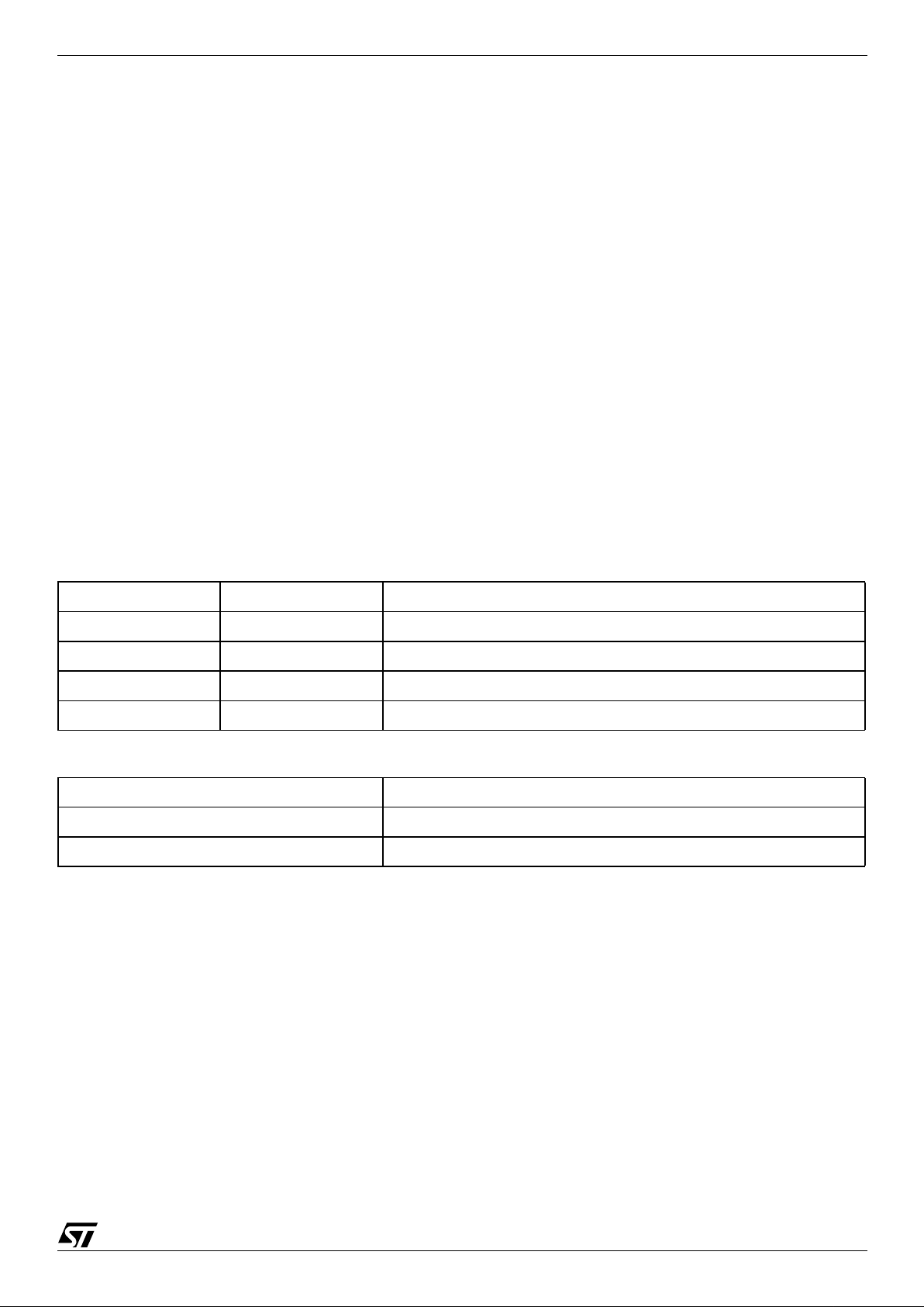
27/175
UPSD3254A, UPSD3254BV, UPSD3253B, UPSD3253BV
External RAM. Table 10 shows a l ist of the Data
Transfer instructions that access external Data
Memory. Only indirect addressing can be used.
The choice is whether t o us e a one-by te address,
@Ri, where Ri can be either R0 or R1 of t he selected register bank, or a two-byte
address, @DTPR.
Note: In all external Data RAM accesses, the Accumulator is always either the destination or
source of the data.
Lookup Ta b les. Table 11 shows the t wo instructions that are available for reading lookup tables in
Program Memory. Since these instructions access
only Program Memory, the lookup tables can only
be read, not updated.
The mnemonic is MOVC for “move constant.” The
first MOVC instruction in Table 11 can accommodate a table of up to 256 entries numbered 0
through 255. The number of the desired e ntry is
loaded into the Accumulator, and the Data Pointer
is set up to point to the beginning of the table.
Then:
MOVC A, @A+DPTR
copies the desired table entry into the Accumulator.
The other MOVC instruction works the same way,
except the Program Counter (PC) is used as the
table base, and the table is accessed through a
subroutine. First the num ber of the desired en-try
is loaded into the Accumulator, and the subroutine
is called:
MOV A , ENTRY NUMBER
CALL TABLE
The subroutine “TABLE” would look like this:
TABLE: MOVC A , @A+PC
RET
The table itself immediately follows the RET (return) instruction is Program Memory. This type of
table can have up to 255 entries, numbered 1
through 255. Number 0 cann ot be used, bec ause
at the time the MOVC instruction is exec uted, the
PC contains the address of the RET instruction.
An entry numbered 0 would be the RET opcode itself.
Table 10. Data Transfer Instruction that Access External Data Memory Space
Table 11. Lookup Table READ Instruction
Address Width Mnemonic Operation
8 bits MOVX A,@Ri READ external RAM @Ri
8 bits MOVX @Ri,A WRITE external RAM @Ri
16 bits MOVX A,@DPTR READ external RAM @DPTR
16 bits MOVX @DPTR,a WRITE external RAM @DPTR
Mnemonic Operation
MOVC A,@A+DPTR READ program memory at (A+DPTR)
MOVC A,@A+PC READ program memory at (A+PC)
UPSD3254A, UPSD3254BV, UPSD3253B, UPSD3253BV
28/175
Boolean Instructions
The uPSD325X dev ices c ontain a c omp lete B oolean (single-bit) processor. One page o f the internal RAM contains 128 address -able bits, and the
SFR space can support up to 128 addressable bits
as well. All of the port lines are bit-addressable,
and each one can be treated as a separate singlebit port. The instructions that access these bits are
not just conditional branches, but a complete
menu of move, set, clear, complement, OR and
AND instructions. These kinds of bit operations
are not easily obtained in other architectures with
any amount of byte-oriented software.
The instruction set for the Boolean processor is
shown in Table 12. All bits acces ses are by di re ct
addressing.
Bit addresses 00h through 7Fh are i n the Lower
128, and bit ad-dresses 80h through FFh are in
SFR space.
Note how easily an internal flag can be moved to
a port pin:
MOV C,FLA G
MOV P1.0,C
In this example, FLAG is the name of any addressable bit in the Lower 128 or SFR space. An I/O
line (the LSB of Port 1, in this case) is set or
cleared depending on whether the Flag Bit is '1' or
'0.'
The Carry Bit in the PSW is used as the single-bit
Accumulator of the Boolean processor. Bit instruction s th a t r efer to th e Ca rr y B it as C as se mbl e a s
Carry-specific instructions (CLR C, etc.). The Carry Bit also has a direct address, since it resides in
the PSW register, which is bit-addressable.
Note: The Boolean instruction set includes ANL
and ORL operations, but not the XRL (Exclusive
OR) operation. An XRL operat ion is simple to implement in software. Suppose, for example, it is required to form the Exclusive OR of two bits:
C = bit 1 .XRL. bit2
The software to do that could be as follows:
MOV C , bit1
JNB bit2, OVER
CPL C
OVER: (continue)
First, Bit 1 is moved to the Carry. If bit2 = 0, then
C now contains the correct result. That is, Bit 1
.XRL. bit2 = bit1 if bit2 = 0. On t he other hand, if
bit2 = 1, C now contains the complement of the
correct result. It need only be inverted (CPL C) to
complete the operation.
This code uses the JNB instruction, one of a series
of bit-test instructions which execute a jump if the
addressed bit is set (JC, JB, JBC) or if the addressed bit is not set (JNC, JNB). In the above
case, Bit 2 is being tested, and if bit2 = 0, the CPL
C instruction is jumped over.
JBC executes the jump if the addressed bit is set,
and also clears the bit. Thus a flag can be tested
and cleared in one operation. All the PSW bits are
directly addressable, so the P arity B it, or the general-purpose flags, for example, are also available
to the bit-test instructions.
Table 12. Boolean Instructions
Relative Offset
The destination address for th ese jumps is spec ified to the assembler by a label or by an actual address in Program memory. How-ever, the
destination address assembl es to a relat ive off set
byte. This is a signed (two’s complement) offset
byte which is added to the PC in two’s complement
arithmetic if the jump is executed.
The range of the jump is therefore -128 to +127
Program Memory bytes relative to the first byte following the instruction.
Mnemonic Operation
ANL C,bit C = A .AND. bit
ANL C,/bit C = C .AND. .NOT. bit
ORL C,bit C = A .OR. bit
ORL C,/bit C = C .OR. .NOT. bit
MOV C,bit C = bit
MOV bit,C bit = C
CLR C C = 0
CLR bit bit = 0
SETB C C = 1
SETB bit bit = 1
CPL C C = .NOT. C
CPL bit bit = .NOT. bit
JC rel Jump if C =1
JNC rel Jump if C = 0
JB bit,rel Jump if bit =1
JNB bit,rel Jump if bit = 0
JBC bit,rel Jump if bit = 1; CLR bit
29/175
UPSD3254A, UPSD3254BV, UPSD3253B, UPSD3253BV
Jump Instructions
Table 13 shows the list of unconditional jump instructions. The table lists a single “JMP add” instruction, but in fact there are three SJMP, LJM P,
and AJMP, which differ in the format of the destination address. JMP is a generic mnemonic which
can be used if the programmer does not care
which way the jump is en-coded.
The SJMP instruction encodes the destination address as a relative offset, as described above. The
instruction is 2 bytes long, consisting of the opcode and the relative offset byte. The jump distance is limited to a range of -128 to +127 bytes
relative to the instruction following the SJMP.
The LJMP instruction encodes the destinat ion address as a 16-bit constant. The instruction is 3
bytes long, cons isting of the op code and two address bytes. The destinati on ad dres s c an b e any where in the 64K Program Memory space.
The AJMP instruction encodes the destination address as an 11-bit constant. The instruction is 2
bytes long, consisting of the opcode, which itself
contains 3 of the 11 address bits, follo wed by another byte containing the low 8 bits of the destination address. When the instruction is executed,
these 11 bits are simply substituted for the low 11
bits in the PC. The high 5 bits stay the same.
Hence the destination has to be within the same
2K block as the instruction following the AJMP.
In all cases the programmer specifies the destination address to the assembler in the same way: as
a label or as a 16-bit constant. The assembler will
put the destination address into the correct format
for the given instruction. If the format required by
the instruction will not support the distan ce to the
specified destination address, a “Destination out
of range” message is written into the List file.
The JMP @A+DPTR instruction supports case
jumps. The destination address is computed at execution time as the sum of the 16-bit DPTR register and the Accumulator. Typically. DPTR is set up
with the address of a jump table. In a 5-way
branch, for ex-ample, an integer 0 through 4 is
loaded into the Accum ulator. The c ode to be executed mi ght be as follows :
MOV DPTR,#JUMP TABLE
MOV A,INDEX_ N U MBER
RL A
JMP @A+DPTR
The RL A instruction converts the index number (0
through 4) to an even number on the range 0
through 8, because each entry in the jump table is
2 bytes long:
JUMP TABLE:
AJMP CASE 0
AJMP CASE 1
AJMP CASE 2
AJMP CASE 3
AJMP CASE 4
Table 13 shows a single “CALL a ddr” instruction,
but there are two of them, LCALL and ACALL,
which differ in the format in which the subroutine
address is given to the CPU. CALL is a generic
mnemonic which c an be used if the prog rammer
does not care which way the address is encoded.
The LCALL instruction uses the 16-bit address format, and the subroutine can be anywh ere in the
64K Program Memory space. The ACALL instruction uses the 11-bit format, and the subroutine
must be in the same 2K block as the instruction following the ACALL.
In any case, the programmer specifies the subroutine address to the assembler in the same way: as
a label or as a 16-bit constant. The assembler will
put the address into the correct format for the given instructions.
Subroutines should end with a RET instruction,
which returns execution to the instruction following
the CALL.
RETI is used to return from an interrupt service
routine. The only difference between RET and
RETI is t hat RETI tells t he int e rru pt control system
that the interrupt in progress is done. If there is no
interrupt in progress at the time RETI is executed,
then the RETI is functionally identical to RET.
Table 13. Unconditional Jump Instructions
Mnemonic Operation
JMP addr Jump to addr
JMP @A+DPTR Jump to A+DPTR
CALL addr Call Subroutine at addr
RET Return from subroutine
RETI Return from interrupt
NOP No operation

UPSD3254A, UPSD3254BV, UPSD3253B, UPSD3253BV
30/175
Table 14 shows the list of conditional jumps available to the uPSD325X device user. All of these
jumps specify the destination address by the relative offset method, and so are limited to a jump distance of -128 to +127 bytes from the instruction
following the conditional jump instruction. Important to note, however, the user specifies to the assembler the actual destination address the same
way as the other jumps: as a label or a 16-bit constant.
There is no Zero Bit in the PSW. The JZ and JNZ
instructions test the Accumulator data for that condition.
The DJNZ instruction (Decrement and Jump if Not
Zero) is for loop control. To execute a loop N
times, load a counter byte with N and terminate the
loop with a DJNZ to t he beginning of the loop, as
shown below for N = 10:
MOV COUNTER,#10
LOOP: (begin loop)
•
•
•
(end loop)
DJNZ COUNTER, LOOP
(continue)
The CJNE instruction (Compare and Jump if Not
Equal) can also be used for loop control as in Table 9. Two bytes are specified in the operand field
of the instruction. The jump is executed only if the
two bytes are not equal. In the example of Table 9
Shifting a BCD Number O ne Digits to the Right,
the two bytes were data in R1 and the constant
2Ah. The initial data in R1 was 2Eh.
Every time the loop was executed, R1 was decremented, and the looping was to continue unt il the
R1 data reached 2Ah.
Another application of this instruction is in “greater
than, less than” comparisons. The two bytes in the
operand field are taken as unsigned integers. If the
first is less than the second, then the Carry Bit is
set (1). If the first is greater than or equal to the
second, then the Carry Bit is cleared
Machine Cycles
A machine cycle consists of a sequence of six
states, numbered S1 through S6. Each state time
lasts for two oscillator periods. Thus, a machine
cycle takes 12 oscillator periods or 1µs if the oscillator frequency is 12MHz. Refer to Figure 14, page
31.
Each state is divided into a Phase 1 half and a
Phase 2 half. State Sequence in uPSD325X devices shows that retrieve/execute sequences in
states and phases for various kinds of instructions.
Normally two program retrievals are generated
during each machine cycle, even if the instruction
being executed does
not
require it. If the instruction being executed does not need more code
bytes, the CPU sim ply ignores the e xtra retrieval,
and the Program Counter is not incremented.
Execution of a one-cycle instruction (Figure 14,
page 31) begins during State 1 of the machine cycle, when the opcode is latched into the Instruction
Register. A second retrieve occurs during S4 of
the same machine cycle. Execution is complete at
the end of State 6 of this machine cycle.
The MOVX instructions take two machine cycles
to execute. No program retrieval is generated during the second cycle of a MOVX instruction. This
is the only time program retrievals are skipped.
The retrieve/execute sequence for MOVX instruction is shown in Figure 14, page 31 (d).
Table 14. Conditional Jump Instructions
Mnemonic Operation
Addressing Modes
Dir. Ind. Reg. Imm
JZ rel Jump if A = 0 Accumulator only
JNZ rel Jump if A ≠ 0 Accumulator only
DJNZ <byte>,rel Decrement and jump if not zero X X
CJNE A,<byte>,rel Jump if A ≠ <byte> X X
CJNE <byte>,#data,rel Jump if <byte> ≠ #data X X

31/175
UPSD3254A, UPSD3254BV, UPSD3253B, UPSD3253BV
Figure 14. State Sequence in uPSD325X Devices
Osc.
(XTAL2)
Read opcode
Read next
opcode
Read next
opcode and
discard
Read next
opcode and
discard
Read 2nd
Byte
No Fetch
No Fetch
No ALE
S1 S2 S3 S4 S5 S6 S1 S2 S3 S4 S5 S6
S1 S2 S3 S4 S5 S6
Read opcode
Read next
opcode
S1 S2 S3 S4 S5 S6
Read opcode
Read next
opcode
S1 S2 S3 S4 S5 S6
Read next
opcode and
discard
S1 S2 S3 S4 S5 S6
Read next
opcode and
discard
Read next
opcode and
discard
Read opcode
(MOVX)
Read next
opcode
S1 S2 S3 S4 S5 S6 S1 S2 S3 S4 S5 S6
Addr Data
Access External Memory
AI06822
p1 p1 p1 p1 p1 p1 p1 p1 p1 p1 p1 p1p2 p2 p2 p2 p2 p2 p2 p2 p2 p2 p2 p2
a. 1-Byte, 1-Cycle Instruction, e.g. INC A
b. 2-Byte, 1-Cycle Instruction, e.g. ADD A, adrs
c. 1-Byte, 2-Cycle Instruction, e.g. INC DPTR
d. 1-Byte, 2-Cycle MOVX Instruction

UPSD3254A, UPSD3254BV, UPSD3253B, UPSD3253BV
32/175
UPSD325X HARDWARE DESCRIPTION
The uPSD325X dev ices hav e a mo dular a rchi tecture with two main func tional mod ules: the MCU
Module and the PSD Mo dule. The MCU Module
consists of a standard 8032 c ore, peripheral s and
other system supporting functions. The PSD Module provides configurable Program and Data memories to the 8032 CPU core. In addition, it has its
own set of I/O ports and a PLD with 16 macrocells
for general logic implementation. Ports A,B,C, and
D are general purpose programmable I/O ports
that have a port architecture which is different from
Ports 0-4 in the MCU Module.
The PSD Module communicates with the CPU
Core through the internal address, data bus (A0A15, D0-D7) and control signals (RD_, WR_,
PSEN_ , ALE, RESET_ ). The u ser def ines the Decoding PLD in the PSDsoft Development Tool and
can map the resourc es i n t he PSD Module to any
program or data address space.
Figure 15. uPSD325X devices Functional Modules
AI07802
4
Channel
ADC
1Mb or 2Mb
Main Flash
Decode PLD
256Kb
SRAM
CPLD - 16 MACROCELLSJTAG ISP
Port 1Port 3
2 UARTs
Interrupt
3 Timer /
Counters
256 Byte SRAM
8032 Core
Port 3, UART,
Intr, Timers,I2C
PSD Internal Bus
8032 Internal Bus
USB
&
Transceiver
Port 1, Timers and
2nd UART and ADC
DDC
w/ 256 Byte
SRAM
PWM
5
Channels
Port 4 PWM
and DDC
Dedicated
USB Pins
Port A & B, PLD
I/O and GPIO
Port D
GPIO
Port C,
JTAG, PLD I/O
and GPIO
VCC, GND,
XTAL
256Kb
Secondary
Flash
Dedicated
Pins
I2C
Port 0, 2
Ext. Bus
Reset Logic
LVD & WDT
Bus
Interface
Reset
D0-D7
A0-A15
RD,PSEN
WR,ALE
Page Register
PSD MODULE
MCU MODULE

33/175
UPSD3254A, UPSD3254BV, UPSD3253B, UPSD3253BV
MCU MODULE DISCRIPTION
This section provides a detail description of the
MCU Module system functions and Peripherals,
including:
– Special Function Registers
– Timers/Counter
– Interrupts
–PWM
– Supervisory Function (LVD and Watchdog)
– USART
– Power Saving Modes
–I
2
C Bus
– On-chip Oscillator
–ADC
–I/O Ports
–USB
Special Function Registers
A map of the on-chip memory area called the Special Function Register (SFR) space is shown in Table 15.
Note: In the SFRs not all of the addresses are occupied. Unoccupied addresses are not implemented on the chip. READ accesses to these
addresses will in gener al retu rn random data, and
WRITE accesses will have no effect. User software should write '0s ' to t hes e unim plement ed locations.
Table 15. SFR Memory Map
Note: 1. Register can be bit addressing
F8 FF
F0
B
(1)
F7
E8
UISTA
(1)
UIEN U CON0 UCON1 UCON2 USTA UAD R UDR0 EF
E0
ACC
(1)
USCL UDT1 UDT0 E7
D8
S1CON
(1)
S1STA S1DAT S1A DR S2CON S2STA S2DAT S2AD R DF
D0
PSW
(1)
S1SETUP S2SETUP RAMBUF DDCDAT DDCA DR DDCCON D7
C8
T2CON
(1)
T2MOD RCAP2 L RCA P2H TL2 TH2 CF
C0
P4
(1)
C7
B8
IP
(1)
BF
B0
P3
(1)
PSCL0L PSCL0H PSCL1L PSCL1H IPA B7
A8
IE
(1)
PWM4P PWM 4W
WDKEY AF
A0
P2
(1)
PWMCON PWM0 PWM1 PWM2 PWM3 WDRST IEA A7
98 SCON SB UF S CON2 SBUF2 9F
90
P1
(1)
P1SFS P3SFS P4SFS ASCL ADAT ACON 97
88
TCON
(1)
TMOD TL0 TL1 TH0 TH 1 8F
80
P0
(1)
SP DPL DP H PCON 87

UPSD3254A, UPSD3254BV, UPSD3253B, UPSD3253BV
34/175
Table 16. List of all SFR
SFR
Addr
Reg Name
Bit Register Name
Reset
Value
Comments
76543210
80 P0 FF Port 0
81 SP 07 Stack Ptr
82 DPL 00 Data Ptr Low
83 DPH 00
Data Ptr
High
87 PCON SMOD SMOD1 LVREN ADSFINT RCLK1 TCLK1 PD IDLE 00 Power Ctrl
88 TCON TF1 TR1 TF0 TR0 IE1 IT1 IE0 IT0 00
Timer / Cntr
Control
89 TMOD Gate C/T M1 M0 Gate C/T M1 M0 00
Timer / Cntr
Mode
Control
8A TL0 00 Timer 0 Low
8B TL1 00 Timer 1 Low
8C TH0 00 Timer 0 High
8D TH1 00 Timer 1 High
90 P1 FF Port 1
91 P1SFS P1S7 P1S6 P1S5 P1S4 00
Port 1 Select
Register
93 P3SFS P3S7 P3S6 00
Port 3 Select
Register
94 P4SFS P4S7 P4S6 P4S5 P4S4 P4S3 P4S2 P4S1 P4S0 00
Port 4 Select
Register
95 ASCL 00
8-bit
Prescaler for
ADC clock
96 ADAT ADAT7 ADAT6 ADAT5 ADAT4 ADAT3 ADAT2 ADAT1 ADAT0 00
ADC Data
Register
97 ACON ADEN ADS1 ADS0 ADST ADSF 00
ADC Control
Register
98 SCON SM0 SM1 SM2 REN TB8 RB8 TI RI 00
Serial
Control
Register
99 SBUF 00 Serial Buffer
9A SCON2 SM0 SM1 SM2 REN TB8 RB8 TI RI 00
2nd UART
Ctrl Register
9B SBUF2 00
2nd UART
Serial Buffer
A0 P2 FF Port 2
A1 PWMCON PWML PWMP PWME CFG4 CFG3 CFG2 CFG1 CFG0 00
PWM
Control
Polarity

35/175
UPSD3254A, UPSD3254BV, UPSD3253B, UPSD3253BV
A2 PWM0 00
PWM0
Output Duty
Cycle
A3 PWM1 00
PWM1
Output Duty
Cycle
A4 PWM2 00
PWM2
Output Duty
Cycle
A5 PWM3 00
PWM3
Output Duty
Cycle
A6 WDRST 00
Watch Dog
Reset
A7 IEA EDDC ES2
EI
2
C
EUSB 00
Interrupt
Enable (2nd)
A8 IE EA - ET2 ES ET1 EX 1 ET 0 EX0 00
Interrupt
Enable
A9
AA PWM4P 00
PWM 4
Period
AB PWM4W 00
PWM 4
Pulse Width
AE WDKEY 00
Watch Dog
Key Register
B0 P3 FF Port 3
B1 PSCL0L 00
Prescaler 0
Low (8-bit)
B2 PSCL0H 00
Prescaler 0
High (8-bit)
B3 PSCL1L 00
Prescaler 1
Low (8-bit)
B4 PSCL1H 00
Prescaler 1
High (8-bit)
B7 IPA PDDC PS2 PI2C PUSB 00
Interrupt
Priority (2nd)
B8 IP PT2 PS PT1 PX1 PT0 PX 0 00
Interrupt
Priority
C0 P4 FF New Port 4
C8 T2CON TF2 EXF2 RCLK TCLK EXEN2 TR2 C/T2 CP/RL2 00
Timer 2
Control
C9 T2MOD DCEN 00
Timer 2
Mode
SFR
Addr
Reg Name
Bit Register Name
Reset
Value
Comments
76543210

UPSD3254A, UPSD3254BV, UPSD3253B, UPSD3253BV
36/175
CA RCAP2L 00
Timer 2
Reload low
CB RCAP2H 00
Timer 2
Reload High
CC TL2 00
Timer 2 Low
byte
CD TH2 00
Timer 2 High
byte
D0 PSW CY AC FO RS1 RS0 OV P 00
Program
Status Word
D1 S1SETUP 00
DDC I
2
C
(S1) Setup
D2 S2SETUP 00
I
2
C (S2)
Setup
D4 RAMBUF XX
DDC Ram
Buffer
D5 DDCDAT 00
DDC Data
xmit register
D6 DDCADR 00
Addr pointer
register
D7 DDCCON — EX_DAT SWENB DDC_AX DDCINT DDC1EN SWHINT M0 00
DDC Control
Register
D8 S1CON CR2 ENI1 STA STO ADDR AA CR1 CR0 00
DDC I
2
C
Control Reg
D9 S1STA GC Stop Intr TX-Md Bbusy Blost ACK_R SLV 00
DDC I
2
C
Status
DA S1DAT 00
Data Hold
Register
DB S1ADR 00
DDC I
2
C
address
DC S2CO N CR2 EN1 STA STO ADDR AA CR 1 CR0 00
I
2
C Bus
Control Reg
DD S2STA GC Stop Intr TX-Md Bbusy Blost ACK_R SLV 00
I
2
C Bus
Status
DE S2DAT 00
Data Hold
Register
DF S2ADR 00
I
2
C address
E0 ACC 00 Accumulator
E1 USCL 00
8-bit
Prescaler for
USB logic
E6 UDT1 UDT1.7 UDT1.6 UDT1.5 UDT1.4 UDT1.3 UDT1.2 UDT1.1 UDT1.0 00
USB Endpt1
Data Xmit
SFR
Addr
Reg Name
Bit Register Name
Reset
Value
Comments
76543210

37/175
UPSD3254A, UPSD3254BV, UPSD3253B, UPSD3253BV
E7 UDT0 UDT0.7 UDT0.6 UDT0.5 UDT0.4 UDT0.3 UDT0.2 UDT0.1 UDT0.0 00
USB Endpt0
Data Xmit
E8 UISTA SUSPND — RSTF TXD0F RXD0F RXD1F EOPF RESUMF 00
USB
Interrupt
Status
E9 UIEN
SUSPNDI
E
RSTE RSTFIE TXD0IE RXD0IE TXD1IE EOPIE
RESUMI
E
00
USB
Interrupt
Enable
EA UCON0 TSEQ0 STALL0 TX0E RX0E TP0SIZ3 TP0SiZ2 TP0SIZ1 TP0SIZ0 00
USB Endpt0
Xmit Control
EB UCON1 TSEQ1 EP12SEL — FRESUM TP1SIZ3 TP1SiZ2 TP1SIZ1 TP1SIZ0 00
USB Endpt1
Xmit Control
EC UCON2 — — — SOUT EP2E EP1E STALL2 STALL1 00
USB Control
Register
ED USTA RSEQ SETUP IN OUT RP0SIZ3 RP0SIZ2 RP0SIZ1 RP0SIZ0 00
USB Endpt0
Status
EE UADR USBEN UADD6 UADD5 UADD4 UADD3 UADD2 UADD1 UADD0 00
USB
Address
Register
EF UDR0 UDR0.7 UDR0.6 UDR0.5 UDR0.4 UDR0.3 UDR0.2 UDR0.1 UDR0.0 00
USB Endpt0
Data Recv
F0 B 00 B Register
SFR
Addr
Reg Name
Bit Register Name
Reset
Value
Comments
76543210

UPSD3254A, UPSD3254BV, UPSD3253B, UPSD3253BV
38/175
Table 17. PSD Module Register Address Offset
CSIOP
Addr
Offset
Register Name
Bit Register Name
Reset
Value
Comments
76543210
00 Data In (Port A) Reads Port pins as input
02 Control (Port A) Configure pin between I/O or Address Out Mode. Bit = 0 selects I/O 00
04 Data Out (Port A) Latched data for output to Port pins, I/O Output Mode 00
06 Direction (Port A) Configures Port pin as input or output. Bit = 0 selects input 00
08 Drive (Port A)
Configures Port pin between CMOS, Open Drain or Slew rate. Bit =
0 selects CMOS
00
0A
Input Macrocell
(Port A)
Reads latched value on Input Macrocells
0C
Enable Out
(Port A)
Reads the status of the output enable control to the Port pin driver.
Bit = 0 indicates pin is in input mode.
01 Data In (Port B)
03 Control (Port B) 00
05 Data Out (Port B) 00
07 Direction (Port B) 00
09 Drive (Port B) 00
0B
Input Macrocell
(Port B)
0D
Enable Out
(Port B)
10 Data In (Port C)
12 Data Out (Port C) 00
14 Direction (Port C) 00
16 Drive (Port C) 00
18
Input Macrocell
(Port C)
1A
Enable Out
(Port C)
11 Data In (Port D) * * * * * *
Only Bit 1 and
2 are used
13 Data Out (Port D) * * * * * * 00
Only Bit 1 and
2 are used
15 Direction (Port D) * * * * * * 00
Only Bit 1 and
2 are used
17 Drive (Port D) * * * * * * 00
Only Bit 1 and
2 are used
1B
Enable Out
(Port D)
***** *
Only Bit 1 and
2 are used
20
Output
Macrocells AB

39/175
UPSD3254A, UPSD3254BV, UPSD3253B, UPSD3253BV
Note: (Register address = csiop address + address offset; where csiop address is defi ned by user in PSDsoft)
* indica tes bit is not used and need to s et to '0.'
21
Output
Macrocells BC
22
Mask Macrocells
AB
23
Mask Macrocells
BC
C0
Primary Flash
Protection
Sec7_
Prot
Sec6_
Prot
Sec5_
Prot
Sec4_
Prot
Sec3_
Prot
Sec2_
Prot
Sec1_
Prot
Sec0_
Prot
Bit = 1 sector
is protected
C2
Secondary Flash
Protection
Security
_Bit
***
Sec3_
Prot
Sec2_
Prot
Sec1_
Prot
Sec0_
Prot
Security Bit =
1 device is
secured
B0 PMMR0 * *
PLD
Mcells
clk
PLD
array-
clk
PLD
Turbo
*
APD
enable
*00
Control PLD
power
consumption
B4 PMMR2 *
PLD
array
Ale
PLD
array
Cntl2
PLD
array
Cntl1
PLD
array
Cntl0
**00
Blocking
inputs to PLD
array
E0 Page 00 Page Register
E2 VM
Periph-
mode
**
FL_
data
Boot_
data
FL_
code
Boot_
code
SR_
code
Configure
8032 Program
and Data
Space
CSIOP
Addr
Offset
Register Name
Bit Register Name
Reset
Value
Comments
76543210

UPSD3254A, UPSD3254BV, UPSD3253B, UPSD3253BV
40/175
INTERRUPT SYSTEM
There are interrupt requests from 10 sources as
follo ws.
■ INT0 external interrupt
■ 2nd USART interrupt
■ Timer 0 interrupt
■ I
2
C interrupt
■ INT1 external interrupt (or ADC interrupt)
■ DDC interrupt
■ Timer 1 interrupt
■ USB interr u p t
■ USART interrupt
■ Timer 2 interrupt
External Int0
■ The INT0 can be either level-active or transition-
active depending on Bit IT0 in register TCON.
The flag that actually generates this interrupt is
Bit IE0 in TCON.
■ When an external interrupt is generated, the
corresponding request flag is cleared by the
hardware when the service routine is vectored
to only if the interrupt was transition activated.
■ If the interrupt was level activated then the
interrupt request flag remains set until the
requested interrupt is actually generated. Then
it has to deactivate the request before the
interrupt service routine is completed, or else
another interrupt will be generated.
Timer 0 and 1 Interrupts
■ Timer 0 and Timer 1 Interrupts are generated by
TF0 and TF1 which are set by an overflow of
their respective Timer/Counter registers (except
for Timer 0 in Mode 3).
■ These flags are cleared by the internal
hardware when the interrupt is serviced.
Timer 2 Inter rupt
■ Timer 2 Interrupt is generated by TF2 which is
set by an overflow of Timer 2. This flag has to be
cleared by the software - not by hardware.
■ It is also generated by the T2EX signal (Timer 2
External Interrupt P1.1) which is controlled by
EXEN2 and EXF2 Bits in the T2CON register.
I
2
C Interrupt
■ The interrupt of the I
2
C is generated by Bit INTR
in the register S2STA.
■ This flag is cleared by hardware.
External Int1
■ The INT1 can be either level active or transition
active depending on Bit IT1 in register TCON.
The flag that actually generates this interrupt is
Bit IE1 in TCON.
■ When an external interrupt is generated, the
corresponding request flag is cleared by the
hardware when the service routine is vectored
to only if the interrupt was transition activated.
■ If the interrupt was level activated then the
interrupt request flag remains set until the
requested interrupt is actually generated. Then
it has to deactivate the request before the
interrupt service routine is completed, or else
another interrupt will be generated.
■ The ADC can take over the External INT1 to
generate an interrupt on conversion being
completed
DDC Interrupt
■ The DDC interrupt is generated either by Bit
INTR in the S1STA register for DC2B protocol
or by Bit DDC interrupt in the DDCCON register
for DDC1 protocol or by Bit SWHINT Bit in the
DDCCON register when DDC protocol is
changed from DDC1 to DDC2.
■ Flags except the INTR have to be cleared by the
software. INTR flag is cleared by hardware.
USB Interrupt
■ The USB interrupt is generated when endpoint0
has transmitted a packet or received a packet,
when endpoint1 or endpoint2 has transmitted a
packet, when the suspend or resume state is
detected and every EOP received.
■ When the USB interrupt is generated, the
corresponding request flag must be cleared by
software. The interrupt service routine will have
to check the various USB registers to determine
the source and clear the corresponding flag.
■ Please see the dedicated interrupt control
registers for the USB peripheral for more
information.

41/175
UPSD3254A, UPSD3254BV, UPSD3253B, UPSD3253BV
USART Int errupt
■ The USART Interrupt is generated by RI
(receive interrupt) OR TI (transmit interrupt).
■ When the USART Interrupt is generated, the
corresponding request flag must be cleared by
software. The interrupt service routine will have
to check the various USART registers to
determine the source and clear the
corresponding flag.
■ Both USART’s are identical, except for the
additional interrupt controls in the Bit 4 of the
additional interrupt control registers (A7H, B7H)
Figure 16. Int errupt System
AI06646
INT0
USART
Timer
0
I2C
INT1
DDC
Timer
1
USB
2nd
USART
Timer
2
High
Low
Interrupt Polling
Interrupt
Sources
IE /
IP / IPA Priority
Global
Enable

UPSD3254A, UPSD3254BV, UPSD3253B, UPSD3253BV
42/175
Table 18. SFR Register
Interrupt Priority Structure
Each interrupt source can be assigned one of two
priority levels. Interrupt priority levels are defined
by the interrupt priority special function register IP
and IPA.
0 = low priority
1 = high priority
A low priority interrupt may be interrupted by a
high priority interrupt level interrupt. A high priority
interrupt routine cannot be interrupted by any other interrupt source. If two interrupts of different priority occur simultaneously, the high priority level
request is serviced. If requests of the same priority
are received simultaneously, an internal polling
sequence determines which request is serviced.
Thus, within each priority level, there is a second
priority structure determined by the polling sequence.
Interrupts Enable Structur e
Each interrupt source can be individua lly enabled
or disabled by setting or clea ring a b it in t he in terrupt enable special function register IE and IEA. All
interrupt source can also b e globally disabled by
clearing Bit EA in IE.
Table 19. Priority Levels
Table 20. Description of the IE Bits
SFR
Addr
Reg
Name
Bit Register Name
Reset
Value
Comments
76543210
A7 IEA EDDC — — ES2 — —
EI
2
C
EUSB 00
Interrupt
Enable (2nd)
A8 IE EA — ET2 ES ET1 EX1 ET0 EX0 00
Interrupt
Enable
B7 IPA PDDC — — PS2 — —
PI
2
C
PUSB 00
Interrupt
Priority (2nd)
B8 IP — — PT2 PS PT1 PX1 PT0 PX0 00
Interrupt
Priority
Source Priority with Level
Int0 0 (highest)
2nd USART 1
Timer 0 2
I²C 3
Int1 4
DDC 5
Timer 1 6
USB 7
1st USART 8
Timer 2+EXF2 9 (lowest)
Bit Symbol Function
7EA
Disable all interrupts:
0: no interrupt with be acknowledged
1: each interrupt source is individually enabled or disabled by setting or clearing its
enable bit
6 — Reserved
5 ET2 Enable Timer 2 Interrupt
4 ES Enable USART Interru pt
3 ET1 Enable Timer 1 Interrupt
2 EX1 Enable External Interrupt (Int1)
1 ET0 Enable Timer 0 Interrupt
0 EX0 Enable External Interrupt (Int0)

43/175
UPSD3254A, UPSD3254BV, UPSD3253B, UPSD3253BV
Table 21. Description of the IEA Bits
Table 22. Description of the IP Bits
Table 23. Description of the IPA Bits
Bit Symbol Function
7 EDDC Enable DDC Interrupt
6 — Not used
5 — Not used
4 ES2 Enable 2nd USART Interrupt
3 — Not used
2 — Not used
1 EI2C Enable I²C Interrup t
0 EU SB Enable USB Interrupt
Bit Symbol Function
7 — Reserved
6 — Reserved
5 PT2 Timer 2 Interrupt priority level
4 PS USART Interrupt priority level
3 PT1 Timer 1 Interrupt priority level
2 PX1 External Interrupt (Int1) priority level
1 PT0 Timer 0 Interrupt priority level
0 PX0 External Interrupt (Int0) priority level
Bit Symbol Function
7 PDDC DDC Interrupt priority level
6 — Not used
5 — Not used
4 PS2 2nd USART Interrupt priority level
3 — Not used
2 — Not used
1 PI2C I²C Interrupt priority level
0 PUSB USB Interrupt priority level

UPSD3254A, UPSD3254BV, UPSD3253B, UPSD3253BV
44/175
How Interrupts are Handled
The interrupt flags are sample d at S5P2 of every
machine cycle . The sa mples a re pol l e d during following machine cycle. If one of the flags was in a
set condition at S5P2 of the preceding cycle, the
polling cycl e will find it and the interrupt system will
generate an LCALL to the appropriate service routine, provided this H/W generated LCALL is not
blocked by any of the following conditions:
■ An interrupt of equal priority or higher priority
level is already in progress.
■ The current machine cycl e i s not th e fi n al cycle
in the execution of the instruction in progress.
■ The instruction in progress is RETI or any
access to the interrupt priority or interrupt
enable registers.
The polling c ycle is repeat ed with each machine
cycle, and the values polled are the values that
were present at S5P2 of the previous machine cycle.
Note: If an interrupt flag is active but being responded to for one of the above mentioned conditions, if the flag is still inact ive when the blocking
condition is removed, the d enied interrupt will not
be serviced. In other words, the fact that the interrupt flag was once active but not serviced is not remembered. Every polling cycle is new.
The processor acknowledges an interrupt request
by executing a hardware generated LCALL to the
appropriate service routine. The hardware generated LCALL pushes the cont ents of the Program
Counter on to the stack (but it does n ot save the
PSW) and reloads the PC with an address that de-
pends on the source of the interrupt being vectored to as shown in Table 24.
Execution proceeds from that location until the
RETI instruction is encountered. The RETI instruction informs the processor that the interrupt routine
is no longer in progress, then pops the top two
bytes from the stack and reloads the Program
Counter. Execution of the interrupted program
continues from where it left off.
Note: A simple RET instruction wo uld also return
execution to the interrupted program, but it would
have left the interrupt control system thinking an
interrup t was still in progr ess , maki ng futu re interrupts impossible.
Table 24. Vector Addresses
Source Vector Address
Int0 0003h
2nd USART 004Bh
Timer 0 000Bh
I²C 0043h
Int1 0013h
DDC 003Bh
Timer 1 001Bh
USB 0033h
1st USART 0023h
Timer 2+EXF2 00 2Bh

45/175
UPSD3254A, UPSD3254BV, UPSD3253B, UPSD3253BV
POWER-SAVING MODE
Two software selectable modes of reduced power
consumption are implemented.
Idle Mode
The following Functions are Switched Off.
– CPU (Halted)
The following Function Rem ain A ctive During Idle
Mode.
– External Interrupts
– Timer 0, Timer 1, Timer 2
– DDC Interface
–PWM Units
– USB Interfa ce
– USART
–8-bit ADC
–I
2
C Interface
Note: Interrupt or RESET
terminates the Idle
Mode.
Power-Down Mode
– System Clock Halted
– LVD Logic Remains Active
– SRAM contents remains unchanged
– The SFRs retain their value until a RESET
is as-
serted
Note: The only way to exit Power-down Mode is a
RESET
.
Table 25. Po wer- S avi ng Mode Power Consumpt i on
Power Control Register
The Idle and Power-down Modes are activated by software via the PCON register.
Table 26. Pi n S ta tus D uri ng Idl e a nd Po we r-down Mode
Table 27. Description of the PCON Bits
Note: 1. See the T2CON register for details of the flag description
Mode Addr/Data Ports1,3,4 PWM
I
2
C
DDC USB
Idle Maintain Data Maintain Data Active Active Active Active
Power-down Maintain Data Maintain Data Disable Disable Disable Disable
SFR
Addr
Reg
Name
Bit Register Name
Reset
Value
Comments
76543210
87 PCON SMOD SMOD1 LVREN ADSFINT RCLK1 TCLK1 PD IDLE 00 Power Ctrl
Bit Symbol Function
7 SMOD Double baud data rate bit UART
6 SMOD1 Double baud data rate bit 2nd UART
5 LVREN LVR disable bit (active High)
4 ADSFINT Enable ADC Interrupt
3
RCLK1
(1)
Received clock flag (UART 2)
2
TCLK1
(1)
Transmit clock flag (UART 2)
1 PD Activate Power-down Mode (High enable)
0 IDL Activate Idle Mode (High enable)

UPSD3254A, UPSD3254BV, UPSD3253B, UPSD3253BV
46/175
Idle Mode
The instruction that sets PCON.0 is the last instruction executed in the normal operating mode
before Idle Mode is activated. Once in the Idle
Mode, the CPU status is preserved in its entirety:
Stack pointer, Program counter, Program status
word, Accumulator, RAM and All other registers
maintain their data during Idle Mode.
There are three ways to terminate the Idle Mode.
■ Activation of any enabled interrupt will cause
PCON.0 to be cleared by hardware terminating
Idle mode. The interrupt is serviced, and
following return from interrupt instruction RETI,
the next instruction to be executed will be the
one which follows the instruction that wrote a
logic '1' to PCON.0.
■ External hardware reset: the hardware reset is
required to be active for two machine cycle to
complete the RESET operation.
■ Internal reset: the microcontroller restarts after
3 machine cycles in all cases.
Power-Down Mode
The instruction that sets PCON. 1 is the last executed prior to going into the Power-down Mode.
Once in Power-down Mode, the oscillator is
stopped. The contents of the on-chip RAM and the
Special Function Register are preserved.
The Power-down Mode can be terminated by an
exter n al R ESET .

47/175
UPSD3254A, UPSD3254BV, UPSD3253B, UPSD3253BV
I/O PORTS (MCU MODULE)
The MCU Module has five ports: Port 0, Port 1,
Port 2, Port 3, and Port 4. (Refer to the PSD Module section on I/O ports A,B,C and D). Ports P0
and P2 are dedicated for the external address and
data bus and is not available in the 52-pin package
devices.
Port 1 - Port 3 are the same as in the standard
8032 micro-controllers, with the exception of the
additional special peripheral functions. All ports
are bi-directional. Pins of which the alternative
function is not used may be used as normal bi-directiona l I/O.
The use of Port 1 -Port 4 pins as alternative functions are carried out automatically by the
uPSD325X devices provided the associat ed SFR
Bit is set HIGH.
The following SFR registers (Tables 29, 30, and
31) are used to control the mapping of alternate
functions onto the I/O port bits. Port 1 alternate
functions are controlled using the P1SFS register,
except for Timer 2 and the 2nd UART which are
enabled by their configuration registers. P1.0 to
P1.3 are default to GPIO after reset.
Port 3 pins 6 and 7 have been modif ied from the
standard 8032. These pins that were used for
READ and WRITE control signals are now GPIO
or I
2
C bus pins. The READ and W RITE pins are
assigned to dedicated pins.
Port 3 (I
2
C) and Port 4 alternate functions are controlled using the P3SFS and P4SFS Special Function Selection registers. A fter a reset , the I/O pins
default to GPIO. The alternate function is enabled
if the corresponding bit in the PXSFS register is
set to '1.' Other Port 3 alternative functions (UART,
Interrupt, and Timer/Counter) are enabled by their
configuration register and do not require setting of
the bits in P3SFS.
Table 28. I/O Port Functions
Table 29. P1SFS (91H)
Table 30. P3SFS (93H)
Table 31. P4SFS (94H)
Port Name Main Function Alternate
Port 1 GPIO
Timer 2 - Bits 0,1
2nd UART - Bits 2,3
ADC - Bits 4..7
Port 3 GPIO
UART - Bits 0,1
Interrupt - Bits 2,3
Timers - Bits 4,5
I
2
C - Bits 6,7
Port 4 GPIO
DDC - Bits 0..2
PWM - Bits 3..7
USB +/- USB +/- Only
76543210
0=Port 1.7
1=ACH3
0=Port 1.6
1=ACH2
0=Port 1.5
1=ACH1
0=Port 1.4
1=ACH0
Bits Reserved Bits Reserved
76543210
0 = Port 3.7
1 = SCL
from I
2
C unit
0 = Port 3.6
1 = SDA
from I2C unit
Bits are reserved.
76543210
0=Port 4.7
1=PWM 4
0=Port 4.6
1=PWM 3
0=Port 4.5
1=PWM 2
0=Port 4.4
1=PWM 1
0=Port 4.3
1=PWM 0
0=Port 4.2
1=V
SYNC
0=Port 4.1
1=DDC -
SCL
0=Port 4.0
1=DDC -
SDA

UPSD3254A, UPSD3254BV, UPSD3253B, UPSD3253BV
48/175
PORT Ty pe and Descript i on
Figure 17. PORT Type and Description (Part 1)
AI06653
Symbol Circuit Description
In /
Out
RESET I
• Schmitt input with internal pull-up
CMOS compatible interface
NFC : 400ns
WR, RD,ALE,
PSEN
O
Output only
XTAL1,
XTAL2
I
O
On-chip oscillator
On-chip feedback resistor
Stop in the power down mode
External clock input available
CMOS compatible interface
PORT0 I/O
Bidirectional I/O port
Schmitt input
Address Output ( Push-Pull )
CMOS compatible interface
NFC
xon

49/175
UPSD3254A, UPSD3254BV, UPSD3253B, UPSD3253BV
Figure 18. PORT Type and Description (Part 2)
AI06654
Symbol Circuit Function
In/
Out
PORT1 <3:0>,
PORT3,
PORT4<7:3,1:0>
PORT2
I/O
PORT4.2
Bidirectional I/O port with internal
pull-ups
Schmitt input
CMOS compatible interface
Bidirectional I/O port with internal
pull-ups
Schmitt input.
TTL compatible interface
Pull-up when reset
Address Latch Enable
Program Strobe Enable
PORT1 < 7:4 > I/O
Bidirectional I/O port with internal
pull-ups
Schmitt input
CMOS compatible interface
Analog input option
I/O
an_enb
USB - ,
USB +
Bidirectional I/O port
Schmitt input
TTL compatible interface
I/O
+
–

UPSD3254A, UPSD3254BV, UPSD3253B, UPSD3253BV
50/175
OSCILLATOR
The oscillator circuit of the uPSD325X devices is a
single stage inverting am plifier in a P ierce o scillator configuration. The circuitry between XTAL1
and XTAL2 is basically a n inverter biased to the
transfer point. Either a crystal or ceramic resonator
can be used as the feedback element to complete
the oscillator circuit. Both are operated in parallel
resonance.
XTAL1 is the high gain amplifier input, and XTAL2
is the output. To drive t he uPSD325X devices ex ternally, XTAL1 is driven from an external source
and XTAL2 left open-circuit.
Figure 19. Oscillator
SUPERVISORY
There are four ways to invoke a reset and initialize
the uPSD325X devices.
■ Via the external RESET pin
■ Via the internal LVR Block.
■ Via USB bus reset signaling.
■ Via Watch Dog timer
The RESET
mechanism is illustrated in Figure 20.
Figure 20. RESET
Configuration
AI06620
XTAL1 XTAL2
8 to 40 MHz
XTAL1 XTAL2
External Clock
AI06621
Reset
CPU
&
PERI.
Noise
Cancel
LVR
S
Q
R
CPU
Clock
Sync
10ms
Timer
USB Reset
RSTE
WDT
PSD_RST
“Active Low
10ms at 40Mhz
50ms at 8Mhz

51/175
UPSD3254A, UPSD3254BV, UPSD3253B, UPSD3253BV
Each RESET source will c ause an inter nal reset
signal active. The CPU responds by executing an
internal reset and puts the internal registers in a
defined state. This internal reset is also routed as
an active low reset input to the PSD Module.
External Reset
The RESET
pin is connected to a S chmitt trigger
for noise reduction. A RESET
is accomplished by
holding the RES ET
pin LOW for at least 1ms at
power up while the oscillator is running. Refer to
AC spec on other RESET
timing requirements.
Low V
DD
Voltage Reset
An internal reset is generated by the LVR circuit
when the V
DD
drops below the reset threshold. Af-
ter V
DD
reaching back up to the re set threshold,
the RESET
signal will remain asserted for 10 ms
before it is released. On initial power-up t he LVR
is enabled (default). After power-up the LVR c an
be disabled via the LVREN Bit in the PCON Register.
Note: The LVR logic is still functio nal in both the
Idle and Power-down Modes.
The reset threshold:
■ 5V operation: 4V +/- 0.25V
■ 3.3V operation: 2.5V +/-0.2V
This logic supports approximately 0.1V of hysteresis and 1µs noise-cancelling delay.
Watchdog Timer Overflow
The Watchdog timer generates an internal reset
when its 22-bit counter overflows. See Watchdog
Timer section for details.
USB Reset
The USB reset is generated by a detec tion on t he
USB bus RESET
signal. A single-end z ero on its
upstream port for 4 to 8 times will set RSTF Bit in
UISTA register. If Bit 6 (RSTE) of the UI EN Register is set, the detection will also generate the
RESET
signal to reset the CPU and other periph-
erals in the MCU.

UPSD3254A, UPSD3254BV, UPSD3253B, UPSD3253BV
52/175
WATCH DOG TI MER
The hardware watchdog timer (WDT) resets the
uPSD325X devices when it overflows. The WDT is
intended as a recovery method in situations where
the CPU may be subjected to a software upset. To
prevent a system reset the timer must be reloaded
in time by the application software. If the processor
suffers a hardware/software malfunc tion, th e sof tware will fail to reload the timer. This failure will result in a reset u pon overflow thus preven ting the
processor running out of control.
In the Idle Mode the watchdog timer and reset circuitry remain active. The WDT consists of a 22-bit
counter, the Watchdog Timer RESET
(WDRST)
SFR and Watchdog Key Register (WDKEY).
Since the WDT is autom atically enabled while the
processor is running. the user only needs to be
concerned with servicing it.
The 22-bit counter overflows when it reaches
4194304 (3FFFFFH). The WDT increments once
every machine cycle.
This means the user must reset the WDT at least
every 4194304 machine cycles (1.258 seconds at
40MHz). To reset the WDT the user must write a
value between 00-7EH to the WDRST register.
The value that is written to the WDRST is loaded
to the 7MSB of the 22 -bit count er. This al lows the
user to pre-loaded the counter to an initial value to
generate a flexible Watchdog time out period.
Writing a “00” to WDRST clears the counter.
The watchdog timer is controlled by the watchdog
key register, WDKEY. Only pattern 01010101
(=55H), disables the watchdog t imer. The rest of
pattern combinations will keep the watchdog timer
enabled. This secur ity key will pr event the wa tchdog timer from being terminated abnormally when
the function of the watchdog timer is needed.
In Idle Mode, the oscillator continues to run. To
prevent the WDT from resetting the processor
while in Idle, the user should always set up a timer
that will periodically exit Idle, service the WDT, and
re-enter Idle Mode.
Table 32. Watchdog Timer Key Register (WDKEY: 0AEH)
Table 33. Description of the WDKEY Bits
76543210
WDKEY7 WDKEY6 WDKEY5 WDKEY4 WDKEY3 WDKEY2 WDKEY1 WDKEY0
Bit Symbol Function
7 to 0
WDKEY7 to
WDKEY0
Enable or disable watchdog timer.
01010101 (=55h): disable watchdog timer. Others: enable watchdog timer

53/175
UPSD3254A, UPSD3254BV, UPSD3253B, UPSD3253BV
Watchdog reset pulse width depends on the clock
frequency. The reset period is Tf
OSC
x 12 x 222.
The RESET
pulse width is Tf
OSC
x 12 x 215.
Figure 21. RESET
Pulse Width
Table 34. Watchdog Timer Clear Register (WDRST: 0A6H)
Table 35. Description of the WDRST Bits
Note: The Watc hdog Timer (WDT) is enabled at power-up or reset and must be served or disabled.
76543210
Reserved WDR ST6 WDRST5 WDRS T4 WDRST3 WDRST2 WDRST1 WDRST0
Bit Symbol Function
7 — Reserved
6 to 0
WDRST6 to
WDRST0
To reset watchdog timer, write any value beteen 00h and 7Eh to this register.
This value is loaded to the 7 most significant bits of the 22-bit counter.
For example: MOV WDRST,#1EH
Reset period
(1.258 second at 40Mhz)
(about 6.291 seconds at 8Mhz)
Reset pulse width (about 10ms at 40Mhz, about 50ms at 8Mhz)
AI06823

UPSD3254A, UPSD3254BV, UPSD3253B, UPSD3253BV
54/175
TIMER/COUNTERS (TIMER 0, TIMER 1 AND TIMER 2)
The uPSD325X devices has three 16-bit Timer/
Counter registers: Timer 0, Timer 1 and Timer 2.
All of them can be configured t o operate either as
timers or event counters and are co mpatible with
standard 8032 architecture.
In the “Timer” function, the register is incremented
every machine cycle. Thus, one can think of it as
counting machine cycles. Since a machine cycle
consists of 6 CPU clock periods, the count rate is
1/6 of the CPU clock frequency or 1/12 o f the oscillator frequency (f
OSC
).
In the “Counter” function, the register is incremented in response to a 1-to-0 transition at its corresponding external input pin, T0 or T1. In this
function, the external input is sampled during
S5P2 of every machine cycle. When the s amples
show a high in one cycle and a low in the next cycle, the count is incremented. The new count value
appears in the register during S3 P1 of the cycle
following the one in which the transition was detected. Since it takes 2 machine cycles (24 f
OSC
clock periods) to recognize a 1-to-0 transition, the
maximum count rate is 1/24 of the f
OSC
. There are
no restriction s on the duty cycl e of the exte rna l input signal, but to ensure that a given level is sampled at least once before it chan ges, it should be
held for at least one full cycle. In addition to t he
“Timer” or “Counter” selection, T imer 0 and Timer
1 have four operating modes from which to select.
Timer 0 and Tim e r 1
The “Timer” or “Counter” function is selected by
control bits C/ T in the Special Function Register
TMOD. These Timer/Counters have four operating modes, which are selected by bit-pairs (M1,
M0) in TMOD. Modes 0, 1, and 2 are the same for
Timers/ Counters. Mode 3 is different. The four operating modes are de-scribed in the following text.
Table 36. Control Register (TCON)
Table 37. Description of the TCON Bits
76543210
TF1 TR1 TF0 TR0 IE1 IT1 IE0 IT0
Bit Symbol Function
7TF1
Timer 1 overflow flag. Set by hardware on Timer/Counter overflow. Cleared by hardware
when processor vectors to interrupt routine
6 TR1 Timer 1 run control bit. Set/cleared by software to turn Timer/Counter on or off
5TF0
Timer 0 overflow flag. Set by hardier on Timer/Counter overflow. Cleared by hardware
when processor vectors to interrupt routine
4 TR0 Timer 0 run control bit. Set/cleared by software to turn Timer/Counter on or off
3IE1
Interrupt 1 Edge Flag. Set by hardware when external interrupt edge detected. Cleared
when interrupt processed
2IT1
Interrupt 1 Type Control Bit. Set/cleared by software to specify falling-edge/low-level
triggered external interrupt
1IE0
Interrupt 0 Edge Flag. Set by hardware when external interrupt edge detected. Cleared
when interrupt processed
0IT0
Interrupt 0 Type Control Bit. Set/cleared by software to specify falling-edge/low-level
triggered external interrupt

55/175
UPSD3254A, UPSD3254BV, UPSD3253B, UPSD3253BV
Mode 0. Putting either Timer into Mode 0 makes
it look like an 8048 Timer, which is an 8-bit Counter
with a divide-by-32 prescaler. Figure 22 shows the
Mode 0 operation as it applies to Timer 1.
In this mode, the Timer register is configured as a
13-bit register. As the count rolls o ve r from al l '1s'
to all '0s,' it sets the Timer Interrupt Flag TF1. The
counted input is enabled to the Timer when TR1 =
1 and either GATE = 0 or /INT1 = 1. (Setting GATE
= 1 allows the Timer to be controlled by external input /INT1, to facilitate pulse width measurements).
TR1 is a control bit in the Special Function Regis-
ter TCON (TCON Control Register). GATE is in
TMOD.
The 13-bit register consists of all 8 bits of TH1 and
the lower 5 bits of TL1. The upper 3 bits of TL1 are
indeterminate and shou ld be ignored. S etting the
run flag does not clear the registers.
Mode 0 operation is the same for t he Timer 0 as
for Timer 1. Substitute TR0, TF0, and /INT0 for the
corresponding Timer 1 signals in Figure 22. There
are two different GAT E Bits, one for Timer 1 and
one for Timer0.
Mode 1. Mode 1 is the same as Mode 0, except
that the Timer register is being run with all 16 bits.
Table 38. TMOD Register (TMOD)
Table 39. Description of the TMOD Bits
76543210
Gate C/T
M1 M0 Gate C/T M1 M0
Bit Symbol Timer Function
7Gate
Timer1
Gating control when set. Timer/Counter 1 is enabled only while INT1 pin is High and
TR1 control pin is set. When cleared, Timer 1 is enabled whenever TR1 control bit is set
6C/T
Timer or Counter selector, cleared for timer operation (input from internal system clock);
set for counter operation (input from T1 input pin)
5 M1 (M1,M0)=(0,0): 13-bit Timer/Counter, TH1, with TL1 as 5-bit prescaler
(M1,M0)=(0,1): 16-bit Timer/Counter. TH1 and TL1 are cascaded. There is no prescaler.
(M1,M0)=(1,0): 8-bit auto-reload Timer/Counter. TH1 holds a value which is to be
reloaded into TL1 each time it overflows
(M1,M0)=(1,1): Timer/Counter 1 stopped
4M0
3Gate
Timer0
Gating control when set. Timer/Counter 0 is enabled only while INT0 pin is High and
TR0 control pin is set. When cleared, Timer 0 is enabled whenever TR0 control bit is set
2C/T
Timer or Counter selector, cleared for timer operation (input from internal system clock);
set for counter operation (input from T0 input pin)
1 M1 (M1,M0)=(0,0): 13-bit Timer/Counter, TH0, with TL0 as 5-bit prescaler
(M1,M0)=(0,1): 16-bit Timer/Counter. TH0 and TL0 are cascaded. There is no prescaler.
(M1,M0)=(1,0): 8-bit auto-reload Timer/Counter. TH0 holds a value which is to be
reloaded into TL0 each time it overflows
(M1,M0)=(1,1): TL0 is an 8-bit Timer/Counter controlled by the standard TImer 0 control
bits. TH0 is an 8-bit timer only controlled by Timer 1 control bits
0M0

UPSD3254A, UPSD3254BV, UPSD3253B, UPSD3253BV
56/175
Figure 22. Ti m er/Counter Mode 0: 13-bit Counter
Figure 23. Timer/Counter Mode 2: 8-bit Auto-reload
AI06622
f
OSC
TF1 Interrupt
Gate
TR1
INT1 pin
T1 pin
Control
TL1
(5 bits)
TH1
(8 bits)
C/T = 0
C/T = 1
÷ 12
AI06623
f
OSC
TF1 Interrupt
Gate
TR1
INT1 pin
T1 pin
Control
TL1
(8 bits)
TH1
(8 bits)
C/T = 0
C/T = 1
÷ 12

57/175
UPSD3254A, UPSD3254BV, UPSD3253B, UPSD3253BV
Figure 24. Timer/Counter Mode 3: Two 8-bit Counters
Mode 2. Mode 2 configures the T im er register as
an 8-bit Counter (TL1) with a utomatic reload, as
shown in Figure 23. Overflow from TL1 not only
sets TF1, but also reloads TL1 with the contents of
TH1, which is preset by software. The reload
leaves TH1 unchanged. Mode 2 operation is the
same for Timer/Counter 0.
Mode 3. Timer 1 in Mode 3 simply holds its count.
The effect is the same as setting TR1 = 0.
Timer 0 in Mode 3 establishes TL0 and TH0 as two
separate counters. The logic for M ode 3 on Tim er
0 is shown in Figure 24. TL0 uses the Timer 0 control Bits: C/T, GATE, TR0, INT0 , and TF0. TH0 is
locked into a timer function (counting machine cycles) and takes over the use of TR1 and TF1 from
Timer 1. Thus, TH0 now controls the “Timer 1“ Interrupt.
Mode 3 is provided for applications requiring an
extra 8-bit timer on the counter. With Timer 0 in
Mode 3, an uPSD325X devices can look like it has
three Timer/Counters. When Timer 0 is in Mode 3,
Timer 1 can be turned on and off by switching it out
of and into its own Mode 3, or can still be used by
the serial port as a baud rate generator, or in fact,
in any application not requiring an interrupt.
Timer 2
Like Timers 0 and 1, Timer 2 can operate as either
an event timer or as an event counter. This is selected by Bit C/T2 in the special function register
T2CON. It has three operating modes: capture,
autoload, and baud rate generator, which are selected by bits in the T2CON as shown in Table 41.
In the Capture Mode there are two options which
are selected by Bit EXEN2 in T2CON. if EXEN2 =
0, then Timer 2 is a 16-bit timer or counter which
upon overflowing sets Bit TF2, the Timer 2 Overflow Bit, which can be used to g enerate an interrupt. If EXEN2 = 1, then Timer 2 still does the
above, but with the added feature that a 1-to-0
transition at external input T2EX causes the current value in the Timer 2 registers, TL2 and TH2,
to be captured into registers RCAP2L and
RCAP2H, respectively. In addition, the transition
at T2EX causes Bit EXF2 in T2CON to be set, and
EXF2 like TF2 can generate an interrupt. The Capture Mode is illustrated in Figure 25.
In the Auto-reload Mode, there are again two options, w h i ch a r e selected by b it EXEN2 in T2CON.
If EXEN2 = 0, then when Timer 2 rolls over it not
only sets TF2 but also causes th e Timer 2 registers to be reloaded with the 16-bit value in registers RCAP2L and RCA P2H, which are preset by
software. If EXEN2 = 1, then Timer 2 still does the
above, but with the added feature that a 1-to-0
transition at external input T2EX will also trigger
the 16-bit reload and set EXF2. The Auto-reload
Mode is illustrated in Standard Serial Interface
(UART) Figure 26. The Baud Rate Generation
Mode is selected by (RCLK, RCLK1)=1 and/or
(TCLK, TCLK1)=1. It will be described in conjunction with the serial port.
AI06624
f
OSC
TF0 Interrupt
Gate
TR0
INT0 pin
T0 pin
Control
TL0
(8 bits)
C/T = 0
C/T = 1
÷ 12
f
OSC
TF1 Interrupt
Control
TH1
(8 bits)
÷ 12
TR1

UPSD3254A, UPSD3254BV, UPSD3253B, UPSD3253BV
58/175
Table 40. Timer/Counter 2 Control Register (T2CON)
Table 41. Description of the T2CON Bits
Note: 1. T he RCLK1 and TCLK1 Bits i n the PCON Re gi ster control UART 2, and have the s am e function as RCLK and TCLK .
76543210
TF2 EXF2 RCL K TCL K EXEN2 TR2 C/T
2 CP/RL2
Bit Symbol Function
7TF2
Timer 2 overflow flag. Set by a Timer 2 overflow, and must be cleared by software. TF2
will not be set when either (RCLK, RCLK1)=1 or (TCLK, TCLK)=1
6EXF2
Timer 2 external flag set when either a capture or reload is caused by a negative
transition on T2EX and EXEN2=1. When Timer 2 Interrupt is enabled, EXF2=1 will
cause the CPU to vector to the Timer 2 Interrupt routine. EXF2 must be cleared by
software
5
RCLK
(1)
Receive clock flag (UART 1). When set, causes the serial port to use Timer 2 overflow
pulses for its receive clock in Modes 1 and 3. TCLK=0 causes Timer 1 overflow to be
used for the receive clock
4
TCLK
(1)
Transmit clock flag (UART 1). When set, causes the serial port to use Timer 2 overflow
pulses for its transmit clock in Modes 1 and 3. TCLK=0 causes Timer 1 overflow to be
used for the transmit clock
3 EXEN2
Timer 2 external enable flag. When set, allows a capture or reload to occur as a result of
a negative transition on T2EX if Timer 2 is not being used to clock the serial port.
EXEN2=0 causes Time 2 to ignore events at T2EX
2 TR2 Start/stop control for Timer 2. A logic 1 starts the timer
1C/T
2
Timer or Counter select for Timer 2. Cleared for timer operation (input from internal
system clock, t
CPU
); set for external event counter operation (negative edge triggered)
0 CP/RL2
Capture/reload flag. When set, capture will occur on negative transition of T2EX if
EXEN2=1. When cleared, auto-reload will occur either with TImer 2 overflows, or
negative transitions of T2EX when EXEN2=1. When either (RCLK, RCLK1)=1 or (TCLK,
TCLK)=1, this bit is ignored, and timer is forced to auto-reload on Timer 2 overflow

59/175
UPSD3254A, UPSD3254BV, UPSD3253B, UPSD3253BV
Table 42. Timer/Counter2 Op erati ng Modes
Note: ↓ = falling edge
Figure 25. Timer 2 in Capture Mode
Mode
T2CON
T2MOD
DECN
T2CON
EXEN
P1.1
T2EX
Remarks
Input Clock
RxCLK
or
TxCLK
CP/
RL
2
TR2 Internal
External
(P1.0/T2)
16-bit
Auto-
reload
0 0 1 0 0 x reload upon overflow
f
OSC
/12
MAX
f
OSC
/24
0010 1↓
reload trigger (falling
edge)
0 0 1 1 x 0 Down counting
0 0 1 1 x 1 Up counting
16-bit
Capture
011x 0x
16-bit Timer/Counter
(only up counting)
f
OSC
/12
MAX
f
OSC
/24
011x 1↓
Capture (TH1,TL2) →
(RCAP2H,RC A P2L)
Baud Rate
Generator
1x1x 0x
No overflow interrupt
request (TF2)
f
OSC
/12
MAX
f
OSC
/24
1x1x 1↓
Extra External Interrupt
(Timer 2)
Off x x 0 x x x Timer 2 stops — —
AI06625
f
OSC
TF2
Capture
TR2
T2 pin
Control
TL2
(8 bits)
TH2
(8 bits)
C/T2 = 0
C/T2 = 1
÷ 12
EXP2
Control
EXEN2
RCAP2L
RCAP2H
T2EX pin
Timer 2
Interrupt
Transition
Detector

UPSD3254A, UPSD3254BV, UPSD3253B, UPSD3253BV
60/175
Figure 26. Timer 2 in Auto-Reload Mode
AI06626
f
OSC
TF2
Reload
TR2
T2 pin
Control
TL2
(8 bits)
TH2
(8 bits)
C/T2 = 0
C/T2 = 1
÷ 12
EXP2
Control
EXEN2
RCAP2L
RCAP2H
T2EX pin
Timer 2
Interrupt
Transition
Detector

61/175
UPSD3254A, UPSD3254BV, UPSD3253B, UPSD3253BV
STANDARD SERIAL INTERFACE (UART)
The uPSD325X devices provides two standard
8032 UART serial ports. The first port is connected
to pin P3.0 (RX) and P3.1 (TX). The second port is
connected to pin P1.2 (RX) and P1.3(TX). The operation of the two serial ports are the same and are
controlled by the SCON and SCON2 registers.
The serial port is full duplex, meaning it can transmit and receive simultaneou sly. It is also receivebuffered, meaning it can commence reception of a
second byte before a previously received byte has
been read from the register. (However, if the f irst
byte still has not been read by the time reception
of the second byte i s complete, one of the bytes
will be lost.) The se rial port receive and transmit
registers are both accessed at Special Function
Register SBUF (or SBUF2 for the second serial
port). Writing to SBU F load s th e t ransmi t re gister,
and reading SBUF accesses a physically separate
receive register.
The serial port can operate in 4 modes:
Mode 0. Serial data enters and exits through
RxD. TxD outputs the shift clock. 8 bits are transmitted/received (LSB first). The b aud rate is fixed
at 1/12 the f
OSC
.
Mode 1. 10 bits are tran smitted (through Tx D) or
received (through RxD): a start B it (0), 8 dat a bi ts
(LSB first), and a Stop Bit (1). On receive, the Stop
Bit goes into RB8 in Special Function Register
SCON. The baud rate is variable.
Mode 2. 11 bits are tran smitted (through Tx D) or
received (through RxD): start Bit (0), 8 data bits
(LSB first), a programmable 9th data bit, and a
Stop Bit (1). O n T ransm it, the 9t h data bi t (TB8 in
SCON) can be as signed the value of '0' or '1. ' O r,
for example, the Parity Bit (P, in the PSW) could
be moved into TB8. On receive, the 9th data bit
goes into RB8 in Special Function Register SCON,
while the Stop Bit is ignored. The baud rate is programmable to either 1/32 or 1/64 the oscillator frequency.
Mode 3. 11 bits are tran smitted (through Tx D) or
received (through RxD): a start B it (0), 8 dat a bi ts
(LSB first), a programmable 9th data bit, and a
Stop Bit (1). In fact, Mode 3 is the same as Mode
2 in all respects except baud ra te. The baud rate
in Mode 3 is variable.
In all four modes, transmission is i nitiated by any
instruction that uses SBUF as a destination register. Reception is initiated in Mode 0 by the co ndition RI = 0 and REN = 1. Reception is initiated in
the other modes by the incoming start bit if REN =
1.
Multiprocessor Commu nicati ons
Modes 2 an d 3 have a specia l provision f or m ultiprocessor communications. In these modes, 9
data bits are received. The 9th one goes into RB8.
Then comes a Stop Bit. The port can be programmed such that when the Stop Bit is received,
the serial port interrupt will be activated only if RB8
= 1. This feature is enabled by setting Bit SM2 in
SCON. A way to use this feature in mul ti-processor systems is as follows:
When the master processor wants to transmit a
block of data to one of several slaves, it first sends
out an address byte which identifies the target
slave. An address byte differs from a dat a byte in
that the 9th bit is '1' in an address byte and 0 in a
data byte. With SM2 = 1, no slave will be interrupted by a data byte. An ad-dress byte, however, will
interrupt all slaves, so t hat eac h slave c an examine the received byte and see if it is being addressed. The addressed slave will clear its SM2
Bit and prepare to receive the d ata bytes that will
be coming. The slaves that weren’t being addressed leave their SM2s set and go on about
their business, ignoring the coming data bytes.
SM2 has no ef fect in Mo de 0, and in Mode 1 can
be used to check the validity of the Stop Bit. In a
Mode 1 reception, if SM2 = 1, the receive interrupt
will not be activ ated un less a valid S top Bit is received.
Serial Port Control Register
The serial port control and status register is the
Special Function Register S CON (SCO N2 for the
second port), shown in Figure 27. This register
contains not only the mode selection bits, but also
the 9th data bit for transmit and receive (TB8 and
RB8), and the Serial Port Interrupt Bits (TI and RI).
Table 43. Serial Port Control Register (SCON)
76543210
SM0 SM1 SM2 REN TB8 RB8 TI RI

UPSD3254A, UPSD3254BV, UPSD3253B, UPSD3253BV
62/175
Table 44. Description of the SCON Bits
Bit Symbol Function
7 SM0 (SM1,SM0)=(0,0): Shift Register. Baud rate = f
OSC
/12
(SM1,SM0)=(1,0): 8-bit UART. Baud rate = variable
(SM1,SM0)=(0,1): 8-bit UART. Baud rate = f
OSC
/64 or f
OSC
/32
(SM1,SM0)=(1,1): 8-bit UART. Baud rate = variable
6SM1
5SM2
Enables the multiprocessor communication features in Mode 2 and 3. In Mode 2 or 3, if
SM2 is set to '1,' RI will not be activated if its received 8th data bit (RB8) is '0.' In Mode
1, if SM2=1, RI will not be activated if a valid Stop Bit was not received. In Mode 0, SM2
should be '0'
4REN
Enables serial reception. Set by software to enable reception. Clear by software to
disable reception
3TB8
The 8th data bit that will be transmitted in Modes 2 and 3. Set or clear by software as
desired
2RB8
In Modes 2 and 3, this bit contains the 8th data bit that was received. In Mode 1, if
SM2=0, RB8 is the Snap Bit that was received. In Mode 0, RB8 is not used
1TI
Transmit Interrupt Flag. Set by hardware at the end of the 8th bit time in Mode 0, or at
the beginning of the Stop Bit in the other modes, in any serial transmission. Must be
cleared by software
0RI
Receive Interrupt Flag. Set by hardware at the end of the 8th bit time in Mode 0, or
halfway through the Stop Bit in the other modes, in any serial reception (except for
SM2). Must be cleared by software

63/175
UPSD3254A, UPSD3254BV, UPSD3253B, UPSD3253BV
Baud Rates. The baud rate in Mode 0 is fixed:
Mode 0 Baud Rate = f
OSC
/ 12
The baud rate in Mo de 2 de pends on the value of
Bit SMOD = 0 (which is the value on reset), the
baud rate is 1/64 the oscillator frequency. If SMOD
= 1, the baud rate is 1/32 the oscillator frequency.
Mode 2 Baud Rate = (2
SMOD
/ 64) x f
OSC
In the uPSD325X devices, the baud rates in
Modes 1 and 3 are determined by the Timer 1
overflow rate.
Using Time r 1 to Ge n e rate Ba ud Ra te s. When
Timer 1 is used as the baud rate generator, the
baud rates in Modes 1 and 3 a re determined by
the Timer 1 overflow rate and the value of SMOD
as follows (see:
Mode 1,3 Baud Rate =
(2
SMOD
/ 32) x (Timer 1 overflow rate)
The Timer 1 Interrupt should be disabled in this
application. The Timer itself can be conf igured for
either “timer” or “counter” operation, a nd in any of
its 3 running modes. In the m ost typical applications, it is configured for “timer” operation, in the
Auto-reload Mode (high nibble of TMOD = 0010B).
In that case the baud rate is given by the formula:
Mode 1,3 Baud Rate =
(2
SMOD
/ 32) x (f
OSC
/ (12 x [256 – (TH1)]))
One can achieve very low baud rates with Timer 1
by leaving the Timer 1 Interrupt enabled, and configuring the Timer to run as a 16-bit t imer (high nibble of TMOD = 0001B), and using the Timer 1
Interrupt to do a 16-bit software reload. Figure 22
lists various commonly use d baud rates and how
they can be obtained from Timer 1.
Using Timer/Counter 2 to Generate Baud
Rates. In the uPSD325X devices, Timer 2 select-
ed as the baud rate generator by setting TCLK
and/or RCLK (see Figure 22, page 56 Timer/
Counter 2 Control Register (T2CON)).
Note: The baud rate for transm it and rece ive can
be simultaneously different. Setting RCLK and/or
TCLK puts Timer into its Baud Rate Generator
Mode.
The RCLK and TCLK Bits in the T2CON register
configure UART 1. The RCLK1 and TCLK1 Bits in
the PCON register configure UART 2.
The Baud Rate Generator Mode is similar to the
Auto-reload Mode, in that a roll over in TH2 causes
the Timer 2 registers to be reloaded with the 16-bit
value in registers RCAP2H and RCAP2L, which
are preset by software.
Now, the baud rates in Modes 1 and 3 are determined at Timer 2’s overflow rate as follows:
Mode 1,3 Baud Rate = Timer 2 Overflow Rate / 16
Table 45. Timer 1-Generated Commonly Used Baud Rates
Baud Rate
f
OSC
SMOD Timer 1
C/T Mode Reload Value
Mode 0 Max: 1MHz 12MHz X X X X
Mode 2 Max: 375K 12MHz 1 X X X
Modes 1, 3: 62.5K 12MHz 1 0 2 FFh
19.2K 11.059MHz 1 0 2 FDh
9.6K 11.059MHz 0 0 2 FDh
4.8K 11.059MHz 0 0 2 FAh
2.4K 11.059MHz 0 0 2 F4h
1.2K 11.059MHz 0 0 2 E8h
137.5 11.059MHz 0 0 2 1Dh
110 6MHz 0 0 2 72h
110 12MHz 0 0 1 FEEBh

UPSD3254A, UPSD3254BV, UPSD3253B, UPSD3253BV
64/175
The timer can be configured for either “timer” or
“counter” operation. In the most typical applications, it is configured for “timer” ope ration (C/T2 =
0). “Timer” operation is a little different for Timer 2
when it’s being used as a baud rate generator.
Normally, as a timer it would increment every machine cycle (thus at the 1/6 the CPU clock frequency). In the case, the baud rate is given by the
formula:
Mode 1,3 Baud Rate =
f
OSC
/ (32 x [65536 – (RCAP2H, RCAP2L)]
where (RCAP2H, RCAP2L) is the content of
RC2H and RC2L taken as a 16-bit unsigned integer.
Timer 2 also be used as the Baud Rate Generating
Mode. This mode is valid only if RCLK + TCLK = 1
in T2CON or in PCON.
Note: A roll-over in TH2 does not set TF2, and will
not generate an interrupt. Therefore, the Timer Interrupt does not have to be disabled when Timer 2
is in the Baud Rate Generator Mode.
Note: If EXEN2 is set, a 1-to-0 transition in T2EX
will set EXF2 but will not cause a reload from
(RCAP2H, RCAP2L) to (TH2, TL2). Thus when
Timer 2 is in use as a baud rate gene rator, T2EX
can be used as an extra e xternal interrupt, if desired.
It should be noted that when Timer 2 is running
(TR2 = 1) in “timer” function in the Baud Rate Generator Mode, one should not try to READ or
WRITE TH2 or TL2. Un der these conditions the
timer is being incremented every state time, and
the results of a READ or WRITE may not be accurate. The RC registers may be read, but should not
be written to, because a WRITE might overlap a
reload and cause WRITE and/or reload errors.
Turn the timer off (clear TR2) before accessing the
Timer 2 or RC registers, in this case.
More Abo ut Mode 0. Serial data enters and exits
through RxD. TxD outputs the shift clock. 8 bits are
transmitted/received: 8 data bits (LSB first). The
baud rate is fixed at 1/12 the f
OSC
.
Figure 27, page 66 shows a simplified func tional
diagram of the serial port in Mode 0, and associated timing.
Transmission is initiated by any instruction that
uses SBUF as a destination register. The “WRITE
to SBUF” signal at S6P2 also loads a '1' into the
9th position of the t ransmit shift register an d tells
the TX Control block to commence a transmission.
The internal timing is such that one full machine
cycle w ill elapse bet ween “WR ITE to SBU F” and
activation of SEND.
SEND enables the output of the shift register to the
alternate out-put function line of RxD and also enable SHIFT CLOCK to the alternate output func-
tion line of TxD. SH IFT CLOC K is lo w during S3,
S4, and S5 of every m ac hine cycle , and high during S6, S1, and S2. At S6P2 of every machine cycle in which SEND is active, the contents of the
transmit shift are shifted to the right one position.
As data bits shift out to the right, zeros come in
from the left. When the M S B of the data byte is at
the output position of the shift register, then the '1'
that was initially loaded into the 9th position, is just
to the left of the MSB, and all positions to the left
of that contain zeros. This condition flags the TX
Control block to do one last shift and t hen deactivate SEND and set T1. Both of these actions occur
at S1P1. Both of these actions occur at S1P1 of
the 10th machine cycle after “WRITE to SBUF.”
Reception is initiated by the condition REN = 1 and
R1 = 0. At S6P2 of th e next machi ne cycl e, the RX
Control unit writes the bits 11111110 to the receive
shift register, and in the next clock phase activates
RECEIVE.
RECEIVE enables SHIFT CLOCK to the alternate
output function line of TxD. SHIFT CLOCK makes
transitions at S3P1 and S6P1 of every machine
cycle in which RECEIVE i s ac tive, the conten ts of
the receive shift register are shifted to the left one
position. The value t hat com es in fr om the right is
the value that was sampled at the RxD pin at S5P2
of the same machine cycle.
As data bits come in from the right, '1s' shift out to
the left. When the '0' that was initially loaded into
the right-most position arrives at the left-most position in the shift register, it flags the RX Control
block to do one last shift and load SBUF. At S1P1
of the 10th machine cycle after the WRITE to
SCON that cleared RI, RECEIVE is cleared as RI
is set.
More Abo ut Mode 1. Ten bits are transmitted
(through TxD), or received (through RxD): a start
Bit (0), 8 data bits (LSB first). and a Stop Bit (1). On
receive, the Stop Bit goes into RB8 in SCON. In
the uPSD325X devices the baud rate is determined by the Timer 1 or Timer 2 over-flow rate.
Figure 29 shows a simplified functional diagram of
the serial port in Mode 1, and assoc iated timings
for transmit receive.
Transmission is initiated by any instruction that
uses SBUF as a destination register. The “WRITE
to SBUF” signal also loads a '1' into the 9th bit position of the transmit shift register and flags the T X
Control unit that a transmission is requested.
Transmission actually c ommenc es at S1P1 of the
machine cycle following the next rollover in the divide-by-16 counter. (Thus, the bit times are synchronized to the divide -by-16 counter, not to the
“WRITE to SBUF” signal.)
The transmission beg ins with activation of SE ND
which puts the start bit at TxD. One bit time later,

65/175
UPSD3254A, UPSD3254BV, UPSD3253B, UPSD3253BV
DATA is activated, which enables the output bit of
the transmit shift register to TxD. The first shift
pulse occurs one bit time after that.
As data bits shift out to the right, zeros are clocked
in from the left. When the MSB of the dat a byt e is
at the output position of the shift register, then the
'1' that was initially loaded into the 9th p osition is
just to the left of the MSB, and all positions to the
left of that cont ain zeros. This c ondition flags t he
TX Control unit to do one last shift and then deactivate SEND and set TI. This occurs at t he 10th divide-by-16 rollover after “WRITE to SBUF.”
Reception is initiated by a detected 1-to-0 transition at RxD. For this purpose RxD is sampled at a
rate of 16 times what ever baud rate has bee n es tablished. When a transition is detected, the divide-by-16 counter is immediately reset, and 1FFH
is written into the input shift register. Resetting the
divide-by-16 counter aligns its roll-overs with the
boundaries of the incoming bit times.
The 16 states of the counter divide each bit time
into 16ths. At t he 7th, 8th, and 9th counter s tates
of each bit time, the bit detector samples the value
of RxD. The value accepted is the value that was
seen in at least 2 of the 3 samples. This is done for
noise rejection. If the value accepted during the
first bit time is not '0,' the receive circuits are reset
and the unit goes back to looking for an-other 1-to0 transition. This is to provide rejection of false
start bits. If the start bit proves valid, it is shifted
into the input shift register, and reception of the reset of the rest of the frame will proceed.
As data bits come in from the right, '1s' shift out to
the left. When the start bit arrives at the left-most
position in the shift register (whi ch in Mode 1 is a
9-bit register), it flags the RX Control block to do
one last shift, load SBUF and RB8, and set RI. The
signal to load SBUF and RB8, and to set RI, will be
generated if, and only if, the following conditions
are met at the time the final shift pulse is gene rated:
1. R1 = 0, and
2. Either SM2 = 0, or the received Stop Bit = 1.
If either of these two condi tions is not m et, the re-
ceived frame is irretrievably lost. If both conditions
are met, the Stop Bit goes into RB8, the 8 data bits
go into SBUF, and RI is activated. At this time,
whether the above condi tions are met or not, the
unit goes back to looking f or a 1-t o-0 transition in
RxD.
More About Modes 2 and 3. Eleven bits are
transmitted (through TxD), or received (through
RxD): a Start Bit (0), 8 data bits (LS B first), a programmable 9th data bit, and a Stop Bit (1). On
transmit, the 9th data b it (TB8) can be assigned
the value of '0' or '1.' On receive, the data bit goes
into RB8 in SCON. The baud rate is programma-
ble to either 1/16 or 1/32 the CPU clock frequency
in Mode 2. Mode 3 may have a variable baud rate
generated from Timer 1.
Figure 31, page 68 a nd Figure 3 3, page 69 s how
a functional diagram of t he serial port in Modes 2
and 3. The receive portion is exactly the same as
in Mode 1. The transmit port ion differs from M ode
1 only in the 9th bit of the transmit shift register.
Transmission is initiated by any instruction that
uses SBUF as a destination register. The “WRITE
to SBUF” signal also loads TB8 into the 9th bit position of the transmit shift register and flags the T X
Control unit that a transmission is requested.
Transmission commences at S1P1 of the machine
cycle following the next roll-over in the divide-by16 counter. (Thus, the bit t imes are synchronized
to the divide-by-16 counter, not to the “WRIT E to
SBUF” signal.)
The transmission be gins w ith ac tivation of SEND,
which puts the start bit at TxD. One bit time later,
DATA is activated, which enables the output bit of
the transmit shift register to TxD. The first shift
pulse occurs one bit time after that. The first shift
clocks a '1' (the Stop Bit) into the 9th bit position of
the shift register. There-after, only zeros are
clocked in. Thus, as data bits shift out to the right,
zeros are clocked in from t he l eft. When TB8 is at
the out-put position of the shift register, then the
Stop Bit is just to the left of TB8, and all positions
to the left of that contain zeros. This condition flags
the TX Control unit to do one last shift and then deactivate SEND and set TI. This occurs at the 11th
divide-by 16 rollover after “WRITE to SUBF.”
Reception is initiated by a detected 1-to-0 transition at RxD. For this purpose RxD is sampled at a
rate of 16 time s what ever baud rate has bee n es tablished. When a transition is detected, the divide-by-16 counter is immediately reset, and 1FFH
is written to the input shift register.
At the 7th, 8th, and 9th counter s tates of eac h bit
time, the bit detector samples the value of R -D.
The value accepted is the value that was seen in
at least 2 of the 3 samples. If the value accepted
during the first bit time is not '0,' the receive circuits
are reset and the unit goes back to looking for another 1-to-0 transition. If the Start Bit proves valid,
it is shifted into the input shift register, and reception of the rest of the frame will proceed.
As data bits come in from the right, '1s' shift out to
the left. When the Start Bit arrives at t he l eft-most
position in the shift register (which in Modes 2 and
3 is a 9-bit register), it flags the RX Control block
to do one last shift, load SBUF and RB8, and set
RI.
The signal to load SBUF a nd RB8, a nd to set RI,
will be generated if, and only if, the following con-

UPSD3254A, UPSD3254BV, UPSD3253B, UPSD3253BV
66/175
ditions are met at the time the final shift pul se is
generated:
1. RI = 0, and
2. Either SM2 = 0, or the received 9th data bit = 1
If either of these conditions is not met, the received
frame is irretrievably lost, and RI is not set. If both
conditions are met, the rec ei ved 9t h dat a bit goes
into RB8, and the first 8 data bits go into SBUF.
One bit time later, whether the above conditions
were met or not, the unit goes back to looking for
a 1-to-0 transition at the RxD input.
Figure 27. Serial Port Mode 0, Block Diagram
AI06824
Zero Detector
Internal Bus
Tx Control
Rx Control
Internal Bus
SBUF
Write
to
SBUF
Read
SBUF
Load
SBUF
SBUF
Input Shift Register
Shift
Shift
Clock
Serial
Port
Interrupt
S6
REN
R1
Rx Clock
Start
Tx Clock
Start
Shift
Shift
Send
Receive
T
R
CL
DS
Q
7 6 5 4 3 2 1 0
RxD
P3.0 Alt
Input
Function
RxD
P3.0 Alt
Output
Function
TxD
P3.1 Alt
Output
Function

67/175
UPSD3254A, UPSD3254BV, UPSD3253B, UPSD3253BV
Figure 28. Serial Port Mode 0, Wavefo rms
Figure 29. Serial Port Mode 1, Block Diagram
AI06825
Write to SBUF
Send
Shift
RxD (Data Out)
TxD (Shift Clock)
T
Write to SCON
RI
Receive
Shift
RxD (Data In)
TxD (Shift Clock)
S6P2
S3P1 S6P1
Clear RI
Receive
Transmit
D0 D1 D2 D3 D4 D5 D6 D7
D0 D1 D2 D3 D4 D5 D6 D7
AI06826
Zero Detector
Internal Bus
Tx Control
Rx Control
Internal Bus
SBUF
Write
to
SBUF
Read
SBUF
Load
SBUF
SBUF
Input Shift Register
Shift
Serial
Port
Interrupt
Rx Clock
Start
Tx Clock
Start
Shift
Shift
Send
Load SBUF
TI
RI
CL
DS
Q
1FFh
TxD
Data
Rx Detector
RxD
1-to-0
Transition
Detector
÷16
Sample
÷16
÷2
TB8
Timer1
Overflow
Timer2
Overflow
0
01
1
01
TCLK
RCLK
SMOD

UPSD3254A, UPSD3254BV, UPSD3253B, UPSD3253BV
68/175
Figure 30. Serial Port Mode 1, Wavefo rms
Figure 31. Serial Port Mode 2, Block Diagram
AI06843
Write to SBUF
Data
Shift
TxD
T1
Rx Clock
RxD
Bit Detector
Sample Times
Shift
RI
S1P1
÷16 Reset
Receive
Transmit
D0 D1 D2 D3 D4 D5 D6 D7
Send
Tx Clock
Start Bit
Stop Bit
D0 D1 D2 D3 D4 D5 D6 D7
Start Bit
Stop Bit
AI06844
Zero Detector
Internal Bus
Tx Control
Rx Control
Internal Bus
SBUF
Write
to
SBUF
Read
SBUF
Load
SBUF
SBUF
Input Shift Register
Shift
Serial
Port
Interrupt
Rx Clock
Start
Tx Clock
Start
Shift
Shift
Send
Load SBUF
TI
RI
CL
DS
Q
1FFh
TxD
Data
Rx Detector
RxD
1-to-0
Transition
Detector
÷16
Sample
÷16
÷2
TB8
Phase2 Clock
1/2*f
OSC
01
SMOD

69/175
UPSD3254A, UPSD3254BV, UPSD3253B, UPSD3253BV
Figure 32. Serial Port Mode 2, Wavefo rms
Figure 33. Serial Port Mode 3, Block Diagram
AI06845
Write to SBUF
Data
Shift
TxD
TI
Rx Clock
RxD
Bit Detector
Sample Times
Shift
RI
S1P1
÷16 Reset
Receive
Transmit
D0 D1 D2 D3 D4 D5 D6 D7
Send
Tx Clock
Start Bit
Stop Bit
TB8
D0 D1 D2 D3 D4 D5 D6 D7
Start Bit
Stop Bit
RB8
Stop Bit
Generator
AI06846
Zero Detector
Internal Bus
Tx Control
Rx Control
Internal Bus
SBUF
Write
to
SBUF
Read
SBUF
Load
SBUF
SBUF
Input Shift Register
Shift
Serial
Port
Interrupt
Rx Clock
Start
Tx Clock
Start
Shift
Shift
Send
Load SBUF
TI
RI
CL
DS
Q
1FFh
TxD
Data
Rx Detector
RxD
1-to-0
Transition
Detector
÷16
Sample
÷16
÷2
TB8
Timer1
Overflow
Timer2
Overflow
0
01
1
01
TCLK
RCLK
SMOD

UPSD3254A, UPSD3254BV, UPSD3253B, UPSD3253BV
70/175
Figure 34. Serial Port Mode 3, Wavefo rms
AI06847
Write to SBUF
Data
Shift
TxD
TI
Rx Clock
RxD
Bit Detector
Sample Times
Shift
RI
S1P1
÷16 Reset
Receive
Transmit
D0 D1 D2 D3 D4 D5 D6 D7
Send
Tx Clock
Start Bit
Stop Bit
TB8
D0 D1 D2 D3 D4 D5 D6 D7
Start Bit
Stop Bit
RB8
Stop Bit
Generator

71/175
UPSD3254A, UPSD3254BV, UPSD3253B, UPSD3253BV
ANALOG-TO-DIGITAL CONVERTOR (ADC)
The analog to digital (A/ D) converter allows conversion of an analog input to a corresponding 8-bit
digital value. The A/D module has four an alog inputs, which are multiplexed into one sample and
hold. The output of the sample and hold is the input into the converter, which generates the result
via successive approximation. The analog supply
voltage is connected to AVREF of ladder resistance of A/D module.
The A/D module has tw o registers which are the
control register ACON and A/D result register
ADAT. The register ACON, shown in Table 47,
page 72, controls the operation of the A/D converter module. To use analog inputs, I/O is selected by
P1SFS register. Also an 8-bit prescaler ASC L divides the main system clock i nput down to approximately 6MHz clock that is required for the ADC
logic. Appropriate values need to be loaded into
the prescaler based upon the main MCU clock frequency prior to use.
The processing of conversion starts when the
Start Bit ADST is set to '1.' After one cycle, it is
cleared by hardware. The register A DAT c ontains
the results of the A/D conversion. When conversion is completed, the result is loaded into the
ADAT the A/D Conversion Status Bit ADSF is set
to '1.'
The block diagram of the A/D module is shown in
Figure 35. The A/D Status Bit ADSF is set automatically when A/D conversion is completed,
cleared when A/D conversion is in process.
The ASCL should be loaded with a value that results in a clock rate of approximately 6MHz for the
ADC using the following formula:
ADC clock input = (f
OSC
/ 2) / (Prescaler register
value +1)
Where f
OSC
is the MCU clock input frequency
The conversion t ime for t he ADC can be calcula ted as follows:
ADC Conversion Time = 8 clock * 8bits * (ADC
Clock) ~= 10.67usec (at 6MHz)
ADC Interrupt
The ADSF Bit in the ACON register is set to '1'
when the A/D conversion is complete. The status
bit can be driven by the MCU, or it can be configured to generate a falling e dge i nterrup t when t he
conversion is complete.
The ADSF Interrupt is enabled by setting the ADSFINT Bit in the PCON register. Once the bit is set,
the external INT1 Interrupt is disabled and the
ADSF Interrupt takes over as INT1. INT1 must be
configured as if it is an edge interrupt input. The
INP1 pin (p3.3) is available for gene ral I/O functions, or Timer1 gate control.
Figure 35. A/D Block Diagram
AI06627
Input
MUX
ACH0
ACH1
ACH2
ACH3
ACON
INTERNAL BUS
ADAT
AVREF
Ladder
Resistor
Decode
S/H
Successive
Approximation
Circuit
Conversion
Complete
Interrupt

UPSD3254A, UPSD3254BV, UPSD3253B, UPSD3253BV
72/175
Table 46. ADC SFR Memory Map
Table 47. Description of the ACON Bits
Table 48. ADC Clock Input
SFR
Addr
Reg
Name
Bit Register Name
Reset
Value
Comments
76543210
95 ASCL 00
8-bit
Prescaler for
ADC clock
96 ADAT ADAT7 ADAT6 ADAT5 ADAT4 ADAT3 ADAT2 ADAT1 ADAT0 00
ADC Data
Register
97 ACON ADEN ADS1 ADS0 ADST ADSF 00
ADC Control
Register
Bit Symbol Function
7 to 6 — Reserved
5
ADEN ADC Enable Bit: 0 : ADC shut off and consumes no operating current
1 : enable ADC
4 — Reserved
3 to 2
ADS1, ADS0 Analog channel select
0, 0 Channel0 (ACH0)
0, 1 Channel1 (ACH1)
1, 0 Channel2 (ACH2)
1, 1 Channel3 (ACH3)
1
ADST ADC Start Bit: 0 : force to zero
1 : start an ADC; after one cycle, bit is cleared to '0'
0
ADSF ADC Status Bit: 0 : A/D conversion is in process
1 : A/D conversion is completed, not in process
MCU Clock Frequency Prescaler Register Value ADC Clock
40MHz 2 6.7MHz
36MHz 2 6MHz
24MHz 1 6MHz
12MHz 0 6MHz

73/175
UPSD3254A, UPSD3254BV, UPSD3253B, UPSD3253BV
PULSE WIDTH MODULATION (PWM)
The PWM block has the following features:
■ Four-channel, 8-bit PWM unit with 16-bit
prescaler
■ One-channel, 8-bit unit with programmable
frequency and pulse width
■ PWM Output with programmable polarity
4-channel PWM Unit (PWM 0-3)
The 8-bit counter of a PWM counts module 256
(i.e., from 0 to 255, inclusive). The valu e held in
the 8-bit counter is compared to the contents of the
Special Function Register (PWM 0-3) of the corresponding PWM. The polarity of the PWM o utputs
is programmable and selected by the PWML Bit in
PWMCON register. Provided the contents of a
PWM 0-3 register is greater than the counter value, the corresponding PWM output is set HIGH
(with PWML = 0). When the contents of this register is less than or equal to the counter value, t he
corresponding PWM output is set LOW (with
PWML = 0). The pulse-width-ratio is therefore de-
fined by the contents of the corresponding Special
Function Register (PWM 0-3) of a PWM. By loading the corresponding Special Function Register
(PWM 0-3) with either 00H or FFH, t he PWM output can be retained at a constant HIGH o r LOW
level respectively (with PWML = 0).
For each PWM unit, there is a 16-bit Prescaler that
are used to divide the main system clock to form
the input clock for the corresponding PWM unit.
This prescaler is used to define the desired repetition rate for the PWM unit. SFR registers B1h B2h are used to hold the 16-bit divisor values.
The repetition frequency of the PWM output is given by:
fPWM
8
= (f
OSC
/ prescaler0) / (2 x 256)
And the input clock frequency to the PWM
counters is = f
OSC
/ 2 / (prescaler data value + 1)
See the I/O PORTS (MCU Module), page 47 for
more information on how to configure the Port 4
pin as PWM output.

UPSD3254A, UPSD3254BV, UPSD3253B, UPSD3253BV
74/175
Figure 36. Four-Channel 8-bit PWM Block Diagram
AI06647
8-bit PWM0-PWM3
Comparators Registers
8-bit PWM0-PWM3
Comparators
8
8
8-bit Counter
x 4
8-bit PWM0-PWM3
Data Registers
8
x 4
Port4.3
Port4.4
Port4.5
Port4.6
Overflow
clock
load
16-bit Prescaler
Register
(B2h,B1h)
16
16-bit Prescaler
Counter
f
OSC
/2
CPU rd/wr
CPU rd/wr
load
PWMCON bit5 (PWME)
PWMCON bit7 (PWML)
4
8
DATA BUS
x 4
8
8

75/175
UPSD3254A, UPSD3254BV, UPSD3253B, UPSD3253BV
Table 49. PWM SFR Memory Map
PWMCON Register Bit Definition:
– PWML = PWM 0-3 polarity control
– PWMP = PWM 4 polarity control
– PWME = PWM enable (0 = disabled, 1= enabl ed)
– CFG3..CF G0 = PWM 0-3 Output (0 = Open Drain; 1 = Push-Pull)
– CFG4 = PWM 4 Output (0 = Open Drain; 1 = Push-Pull)
SFR
Addr
Reg Name
Bit Register Name
Reset
Value
Comments
76543210
A1 PWMCON PWML PWMP PWME CFG4 CFG3 CFG2 CFG1 CFG0 00
PWM
Control
Polarity
A2 PWM0 00
PWM0
Output
Duty Cycle
A3 PWM1 00
PWM1
Output
Duty Cycle
A4 PWM2 00
PWM2
Output
Duty Cycle
A5 PWM3 00
PWM3
Output
Duty Cycle
AA PWM4P 00
PWM 4
Period
AB PWM4W 00
PWM 4
Pulse
Width
B1 PSCL0L 00
Prescaler 0
Low (8-bit)
B2 PSCL 0H 00
Prescaler 0
High (8-bit)
B3 PSCL 1L 00
Prescaler 1
Low (8-bit)
B4 PSCL 1H 00
Prescaler 1
High (8-bit)

UPSD3254A, UPSD3254BV, UPSD3253B, UPSD3253BV
76/175
Programm a b le P eri od 8 -bi t PW M
The PWM 4 chan nel can be programmed to provide a PWM output with variable pulse wi dth and
period. The PWM 4 has a 16-bi t Prescaler, an 8bit Counter, a Pulse Wid th Regist er, and a Period
Register. The Pulse Width Register defines the
PWM pulse width time, while the Pe riod Register
defines the period of t he PWM . The input clock t o
the Prescaler is f
OSC
/2. The PWM 4 channel is as-
signed to Port 4.7.
Figure 37. Programmable PWM 4 Channel Block Diagram
AI07091
Port 4.7
16-bit Prescaler
Register
(B4h, B3h)
16-bit Prescaler
Counter
8-bit Counter
8-bit PWM4P
Register
(Period)
8-bit PWM4
Comparator
Register
8-bit PWM4
Comparator
PWM4
Control
Match
CPU RD/WR
Load
Load
Clock
Reset
PWMCON
Bit 6 (PWMP)
DATA BUS
CPU RD/WR
f
OSC
/ 2
PWMCON
Bit 5 (PWME)
8
16
8
8
8
8
8-bit PWM4W
Register
(Width)
8-bit PWM4
Comparator
Register
8-bit PWM4
Comparator
8
88
8
8

77/175
UPSD3254A, UPSD3254BV, UPSD3253B, UPSD3253BV
PWM 4 Channel Operation
The 16-bit Prescaler1 divides the input clock
(f
OSC
/2) to the desired frequency, the resulting
clock runs the 8-bit Counter of the PWM 4 channel. The input clock frequency to the PWM 4
Counter is:
f PWM 4 = (f
OSC
/2)/(Prescaler1 data value +1)
When the Prescaler1 Register (B4h, B3h) is set to
data value '0,' the maximum input clock frequency
to the PWM 4 Counter is f
OSC
/2 and can be as high
as 20MHz.
The PWM 4 Counter is a free-running, 8-bit
counter. The output of the coun ter is compared t o
the Compare Registers, which are loaded with
data from the Pulse Width Register (PWM4W,
ABh) and the Period Register (PWM4P, AAh). The
Pulse Width Register defines the pulse duration or
the Pulse Width, while the Period Register defines
the period of the PWM. When the PWM 4 channel
is enabled, the register val ues are l oaded int o the
Comparator Registers and are compared to the
Counter output. When the content of the counter is
equal to or greater than the value in the Pulse
Width Register, it sets the PWM 4 output t o low
(with PWMP Bit = 0). When the Period Register
equals to the PWM4 Counter, the Counter is
cleared, and the PWM 4 channel output is set to
logic 'high' level (beginning of the next PWM
pulse).
The Period Register cann ot have a value of “00”
and its content should always be greater than the
Pulse Width Register.
The Prescaler1 Register, Pulse Width Register,
and Period Register can be modified while the
PWM 4 channel is active. The values of these registers are automatically loaded into the Prescaler
Counter and Comparator Registers when the current PWM 4 period ends.
The PWMCON Register (Bits 5 and 6) controls the
enable/disable and polarity of the PWM 4 channel.
Figure 38. P WM 4 With Prog ram m a b le P ul s e Width and Freq ue n c y
AI07090
PWM4
Defined by Pulse
Width Register
Switch Level
RESET
Counter
Defined by Period Register

UPSD3254A, UPSD3254BV, UPSD3253B, UPSD3253BV
78/175
I2C INTERFACE
There are two serial I
2
C ports impl eme nted in the
uPSD325X devices.
The serial port supports the twin line I
2
C-bus, consists of a data line (SDAx) and a clock line (SCLx).
Depending on the configuration, the SDA and SCL
lines may require pull-up resistors.
■ SDA1, SCL1: the serial port line for DDC
Protocol
■ SDA2, SCL2: the serial port line for general I
2
C
bus connection
In both I
2
C interfaces, these lines also function as
I/O port lines as follows.
■ SDA1 / P4. 0, SCL 1 / P4.1, SDA2 / P3. 6, SCL2 /
P3.7
The system is unique because data transport,
clock generation, address recognition and bus
control arbitration are all controlled by hardware.
The I
2
C serial I/O has complete autonomy in byte
handling and operates in 4 modes.
■ Master transmitter
■ Master receiver
■ Slave transmitter
■ Slave receiver
These functions are controlled by the SFRs.
■ SxCON: the control of byte handling and the
operation of 4 mode.
■ SxSTA: the contents of its register may also be
used as a vector to various service routines.
■ SxDAT: data shift register.
■ SxADR: slave address register. Slave address
recognition is performed by On-Chip H/W.
Figure 39. Block Diagram of the I
2
C Bus Serial I/O
AI06649
SCLx
SDAx
Bus Clock Generator
Arbitration and Sync. Logic
Shift Register
Status Register
70
Slave Address
70
Control Register
70
70
Internal Bus

79/175
UPSD3254A, UPSD3254BV, UPSD3253B, UPSD3253BV
Table 50. Serial Control Register (SxCON: S1CON, S2CON)
Table 51. Description of the SxCON Bits
Table 52. Selection of the Serial Clock Frequency SCL in Master Mode
76543210
CR2 ENII STA STO ADDR AA CR1 CR0
Bit Symbol Function
7CR2
This bit along with Bits CR1and CR0 determines the serial clock frequency when SIO is
in the Master Mode.
6ENII
Enable IIC. When ENI1 = 0, the IIC is disabled. SDA and SCL outputs are in the high
impedance state.
5STA
START flag. When this bit is set, the SIO H/W checks the status of the I
2
C-bus and
generates a START condition if the bus free. If the bus is busy, the SIO will generate a
repeated START condition when this bit is set.
4STO
STOP flag. With this bit set while in Master Mode a STOP condition is generated.
When a STOP condition is detected on the I
2
C-bus, the I2C hardware clears the STO
flag.
Note: This bit have to be set before 1 cycle interrupt period of STOP. That is, if this bit is
set, STOP condition in Master Mode is generated after 1 cycle interrupt period.
3 ADDR This bit is set when address byte was received. Must be cleared by software.
2AA
Acknowledge enable signal. If this bit is set, an acknowledge (low level to SDA) is
returned during the acknowledge clock pulse on the SCL line when:
• Own slave address is received
• A data byte is received while the device is programmed to be a Master Receiver
• A data byte is received while the device is a selected Slave Receiver. When this bit is
reset, no acknowledge is returned.
SIO release SDA line as high during the acknowledge clock pulse.
1CR1
These two bits along with the CR2 Bit determine the serial clock frequency when SIO is
in the Master Mode.
0CR0
CR2 CR1 CR0
f
OSC
Divisor
Bit Rate (kHz) at f
OSC
12MHz 24MHz 36MHz 40MHz
0 0 0 16 375 750 X X
0 0 1 24 250 500 750 833
0 1 0 30 200 400 600 666
0 1 1 60 100 200 300 333
1 0 0 120 50 100 150 166
1 0 1 240 25 50 75 83
1 1 0 480 12.5 25 37.5 41
1 1 1 960 6.25 12.5 18.75 20

UPSD3254A, UPSD3254BV, UPSD3253B, UPSD3253BV
80/175
Serial Status Reg i s t e r ( SxSTA : S1STA, S2STA )
SxSTA is a “Read-only” register. The contents of
this register may be used as a vector to a service
routine. This optimized the response time of the
software and consequently that of the I
2
C-bus.
The status codes for all possible modes of the I
2
C-
bus interface are given Table 54.
This flag is set, and an interrupt is generated, after
any of the following events occur.
1. Own slave address has been received during
AA = 1: ack_int
2. The general call address has been received
while GC(SxADR.0) = 1 and AA = 1:
3. A data byte has been received or transmitted in
Master Mode (even if arbitration is lost): ack_int
4. A data byte has been received or transmitted as
selected slave: ack_int
5. A stop condition is recei ved as selected slave
receiver or transmitter: stop_int
Data Shift Register (SxDAT: S1DAT, S2DAT)
SxDAT contains the serial data to be transmitted
or data which has just been received. The MSB
(Bit 7) is transm itted or received first; that is, data
shifted from right to left.
Table 53. Serial Status Register (SxSTA)
Table 54. Description of the SxSTA Bits
Note: 1. Interrupt F l ag Bit (INTR, SxSTA Bit 5) is cleared by Hardware as readin g SxSTA regi st er.
2. I
2
C interrupt flag (I NT R) can occ ur i n below case. (except DDC2B Mode at SWENB= 0)
Table 55. Data Shift Register (SxDAT: S1DAT, S2DAT)
76543210
GC STOP INTR TX_MODE BBUSY BLOST /ACK_REP SLV
Bit Symbol Function
7 GC General Call Flag
6 STOP Stop Flag. This bit is set when a STOP condition is received
5
INTR
(1,2)
Interrupt Flag. This bit is set when an I²C Interrupt condition is requested
4 TX_MODE
Transmission Mode Flag.
This bit is set when the I²C is a transmitter; otherwise this bit is reset
3 BBUSY
Bus Busy Flag.
This bit is set when the bus is being used by another master; otherwise, this bit is reset
2 BLOST
Bus Lost Flag.
This bit is set when the master loses the bus contention; otherwise this bit is reset
1 /ACK_REP
Acknowledge Response Flag.
This bit is set when the receiver transmits the not acknowledge signal
This bit is reset when the receiver transmits the acknowledge signal
0SLV
Slave Mode Flag.
This bit is set when the I²C plays role in the Slave Mode; otherwise this bit is reset
76543210
SxDAT7 SxDAT6 SxDAT5 SxDAT4 SxDAT3 SxDAT2 SxDAT1 SxDAT0

81/175
UPSD3254A, UPSD3254BV, UPSD3253B, UPSD3253BV
Address Register (SxADR: S1ADR, S2ADR)
This 8-bit register may be loaded with the 7-bit
slave address to which the controller will respond
when programmed as a slave receive/transmitter.
The Start/Stop Hold Time Detection and Sy stem
Clock registers (Tables 57 and 58) are included in
the I
2
C unit to specify the start/stop detection time
to work with the large range of MCU frequency values supported. For example, with a system clock
of 40MHz.
Table 56. Address Register (SxADR)
Note: 1. SLA6 to SLA0: Own slave address.
Table 57. Start /Stop Hold Time Detection Register (S1SETUP, S2SETUP)
Table 58. System Cock of 40MHz
Tab le 59. System Clock Setup Exam ples
76543210
SLA6 SLA5 SLA4 SLA3 SLA2 SLA1 SLA0 —
Address Register Name Reset Value Note
SFR
D1h S1SETUP 00h
To control the start/stop hold time detection for the DDC module
in Slave Mode
D2h S2SETUP 00h
To control the start/stop hold time detection for the multi-master
I²C module in Slave Mode
S1SETUP,
S2SETUP Register
Value
Number of Sample
Clock (f
OSC
/2 ->
50ns)
Required Start/
Stop Hold Time
Note
00h 1EA 50ns
When Bit 7 (enable bit) = 0, the number of
sample clock is 1EA (ignore Bit 6 to Bit 0)
80h 1EA 50ns
81h 2EA 100ns
82h 3EA 150ns
... ... ...
8Bh 12EA 600ns Fast Mode I²C Start/Stop hold time specification
... ... ...
FFh 128EA 6000ns
System Clock
S1SETUP,
S2SETUP Register
Value
Number of Sample
Clock
Required Start/Stop Hold Time
40MHz (f
OSC
/2 -> 50ns)
8Bh 12 EA 600ns
30MHz (f
OSC
/2 -> 66.6ns)
89h 9 EA 600ns
20MHz (f
OSC
/2 -> 100ns)
86h 6 EA 600ns
8MHz (f
OSC
/2 -> 250ns)
83h 3 EA 750ns

UPSD3254A, UPSD3254BV, UPSD3253B, UPSD3253BV
82/175
DDC INTERFACE
The basic DDC unit consists of an I
2
C interface
and 256 bytes of SRAM for DDC data storage. The
8032 core is responsible of loading the contents of
the SRAM with the DDC data. The DDC unit has
the following features:
■ Supports both DDC1 and DDC2b Modes.
■ Features 256 bytes of DDC data - initialized by
the 8032
■ Supports fully automatic operation of DDC1 and
DDC2b Modes
■ DDC operates in Slave Mode only.
■ SW Interrupt Mode available (existing design)
The interface signals for the DDC can be mapped
to pins in Port 4. The interface consists of the standard V
SYNC
(P4.2), SDA (P4.0) and SCL (P4.1)
DDC signals. The conceptual block diagram is illustrated in Figure 43.
Figure 40. DDC Interface Block Diagram
AI06628
INT
DDCCON
INTR (from SISTA)
Initialization Synchronization
DDCADR
Address Pointer
RAM
Buffer
RAMBUF
VSYNC
EN
DDC1 Transmitter
DDCDAT
DDC1 Hold Register
DDC1/DDC2
Detection
SISTA
SICON
SCL1
SDA1
Bus Clock Generator
Arbitration Logic
S1DAT
S1ADR1
S1ADR0
Shift Register
DDC2B/DDC2AB
DDC2B+Interface
Internal Bus
Monitor Address
Monitor Address
7 10
XX
EX_
DATSWENB
DDC1
INT
DDC1ENSWH
INT
M0

83/175
UPSD3254A, UPSD3254BV, UPSD3253B, UPSD3253BV
Special Function Register for the DDC Interface
There are eight SFR in the DDC interface:
RAMBUF, DDCCON, DDCADR, DDCDAT are
DDC registers.
S1CON, S1STA, S1DAT, S1ADR are I
2
C Interface registers, same as the ones desc ribed in t he
standalone I
2
C bus.
DDCDAT Register. DDC1 DATA register for
transmission (DDCDAT: 0D5H)
■ 8-bit READ and WRITE register.
■ Indicates DATA BYTE to be transmitted in
DDC1 protocol.
DDCADR Register. Address pointer for DDC interface (DDCADR: 0D6H)
■ 8-bit READ and WRITE register.
■ Address pointer with the capability of the post
increment. After each a ccess to RAMBUF
register (either by software or by hardware
DDC1 interface), the content of this register will
be increased by one. It’s available both in
DDC1, DDC2 (DDC2B, DDC2B+, and
DDC2AB) and system operation.
Table 60. DDC SFR Memory Map
SFR
Addr
Reg
Name
Bit Register Name
Reset
Value
Comments
76543210
D4 RAMBUF XX
DDC Ram
Buffer
D5 DDCDAT 00
DDC Data
xmit register
D6 DDCADR 00
Addr pointer
register
D7 DDCCON — EX_DAT SWENB DDC_AX DDCINT DDC1EN SWHINT M0 00
DDC Control
Register

UPSD3254A, UPSD3254BV, UPSD3253B, UPSD3253BV
84/175
Table 61. Description of the DDCON Register Bits
Bit Symbol Function
7 — Reserved
6 EX_DAT
0 = The SRAM has 128 bytes (Default)
1 = The SRAM has 256 bytes
5 SWENB
Note: This bit is valid for DDC1 & DDC2b Modes
0 = Data is automatically read from SRAM at the current location of DDCADR and sent
out via current DDC protocol. (Default)
1 = MCU is interrupted during the current data byte transmission period to load the next
byte of data to send out.
4 DDC_AX
Note: This bit is valid for DDC1 & DDC2b Modes
0 = Data is automatically read from SRAM at the current location of DDCADR and sent
out via current DDC protocol. (Default)
1 = MCU is interrupted during the current data byte transmission period to load the next
byte of data to send out.
This bit only affects DDC2b Mode Operation:
0 = DDC2b I2C Address is A0/A1 (default)
1 = DDC2b I2C Address is AX. Least 3 significant address bits are ignored.
3 DDC1_Int
For DDC1 Mode Operation Only:
0 = No DDC1 Interrupt
1 = DDC1 Interrupt request. Set by HW and should be cleared by SW interrupt service
routine.
Note1: This bit is set in the 9th V
CLK
at DDC1 Enable Mode. (SWENB=1)
2 DDC1EN
0 = DDC1 Mode is disabled – V
SYNC
is ignored.
The DDC unit will still respond to DDC2b requests. –provided I2C enabled.(Default)
1 = DDC1 Mode is enabled.
1 SWHINT
Set by hardware when the DDC unit switches from DDC1 to DDC2b Modes.
0 = No interrupt request.
1 = Switch to DDC2b Mode (Interrupt pending)
Set by HW and should be cleared by SW interrupt service routine.
Note1: This bit has no connection with SWENB.
0Mode
Current Mode Indication Bit:
0 = Unit is in DDC1 Mode
1 = Unit is in DDC2b Mode
Note: When the DDC unit transitions to DDC2b Mode, the DDC unit will stay in DDC2b
Mode until the DDC unit is disabled, or the system is reset.

85/175
UPSD3254A, UPSD3254BV, UPSD3253B, UPSD3253BV
Table 62. SWNEB Bit Function
SWENB
DDC1 or DDC2b Mode Disabled DDC1 or DDC2b Mode Enabled
DDCCON.bit2 = 0 (DDC1 Mode Disable) or
S1CON.bit6 = 0 (I
2
C Mode Disable)
DDCCON.bit2 = 1 (DDC1 Mode Enable) or
S1CON.bit6 = 1 (I2C Mode Enable)
0
In this state, the DDC unit is disabled. The DDC
SRAM cannot be accessed by the MCU. No MCU
interrupt and no DDC activity will occur.
MCU cannot access internal DDC SRAM: DDC
SRAM address space is re-assigned to external
data space.
In this state, the DDC is enabled and the unit is in
automatic mode. The DDC SRAM cannot be
accessed by the MCU – only the DDC unit has
access.
MCU cannot access internal DDC SRAM: data
space FF00h-FFFFh is dedicated to DDC SRAM.
1
In this state, the DDC unit is disabled, BUT with
SWENB=1, the MCU can access the SRAM. This
state is used to load the DDC SRAM with the
correct data for automatic modes. No MCU
interrupt and no DDC activity will occur.
MCU can access DDC SRAM: data space FF00hFFFFh is dedicated to DDC SRAM.
In this state, the DDC SRAM can be accessed by
the MCU. The DDC unit does not use the DDC
SRAM when SWENB=1. Since the DDC unit is in
manual mode, the DDC unit generates an MCU
interrupt for each byte transferred. The byte
transferred is held in the I
2
C S1DAT SFR register.
MCU can access DDC SRAM.

UPSD3254A, UPSD3254BV, UPSD3253B, UPSD3253BV
86/175
Host Type Detection
The detection procedure conforms to the sequences proposed by VESA Monitor Display Da ta
Channel (DDC) specification. The monitor needs
to determine the type of host system:
■ DDC1 or OLD type host.
■ DDC2B host (Host is master, monitor i s al ways
slave)
■ DDC2B+/DDC2AB(ACCESS.bus) host.
Figure 41. Host Type Det ec ti on
AI06644
Is VSYNC present?
Has a command
been received?
Is 2B+/A.B
command detected?
Is
DDC2B+/DDC2AB?
Is it DDC2B
command?
Power on
Communication
isidle
EDID sent continously using
VSYNC as clock
Is DDC2 clock
present?
Stop sending of EDID
switch to DDC2
communication mode
DDC2 communication
is idle.
Respond to
DDC2B command
Respond to DDC2B+/
DDC2AB command

87/175
UPSD3254A, UPSD3254BV, UPSD3253B, UPSD3253BV
DDC1 Protocol
DDC1 is primitive and a point to point interface.
The monitor is always put at “Transmit only” mode.
In the initialization phase, 9 clock cycles on V
CLK
pin will be given for the internal synchronization.
During this period, the SDA pin will be kept at high
impedance state.
If DDC1 hardware mode is used, the following pro-
cedure is recommended to proceed DDC1 operation.
1. Reset DDC1 enable (by default, DDC1 enable is
cleared as LOW after Power-on Reset).
2. Set SWENB as high (the default value is zero.)
3. Depending on the data size of EDID data, set
EX_DAT as LOW (128 bytes) or HIGH (256
bytes).
4. By using bulky moving commands (DDCADR,
RAMBUF involved) to move the entire EDID
data to RAM buffer.
5.Reset SWENB to LOW.
6. Reset DDCADR to 00h.
7. Set DDC1 enable as HIGH.
In case SWENB is set as high, interrupt service
routine is finished within 133 machine cycle in
40MHz System clock.
The maxi mum V
SYNC
(V
CLK
) frequency is 25Khz
(40µs). And the 9th clock of V
SYNC
(V
CLK
) is inter-
rupt period.
So the machine cycle b e needed is calculated as
below. For example,
When 40MHz system clock, 40µs = 133 x (25ns x
12); 133 machine cycle.
12MHz system clock, 40µs = 40 x (83.3ns x 12);
40 machine cycle.
8MHz system clock, 40µs = 26 x (125ns x 12); 26
machine cycle.
Note: If EX_DAT equals to LOW , it is meant the
lower part is occupied by DDC1 operation and the
upper part is still free t o the system. Nevertheless,
the effect of the post increm ent j ust appli es t o t he
part related to DDC1 operation. In other words, the
system program is still able to address the locations from 128 to 255 in the RAM buffer through
MOVX command but without the facility of the post
increment. For example, the case of accessing
200 of the RAM Buffer:
MOV R0, #200, and
MOVX A, @R0
Figure 42. Transmission Protocol in the DDC1 Interface
AI06652
1234567891234567891
B
t
SU(DDC1)
t
DOV
Hi-Z
SC
VCLK
DDC1INT
DDC1EN
SD
t
H(VCLK)
t
L(VCLK)
Max=40us
BBBBBBB BHiZ

UPSD3254A, UPSD3254BV, UPSD3253B, UPSD3253BV
88/175
DDC2B Protocol
DDC2B is constructed based on the Philips I
2
C in terface. However, in the level of DDC2B, PC host
is fixed as the master and t he monitor is always regarded as the slave. Both master and slave can be
operated as a transmitter or receiver, but the master device determines which mod e is activated. In
this protocol, address pointer is also used.
According to DDC2B specification, A0 (for WRITE
Mode) and A1 (for READ Mode) are assigned as
the default address of monitors.
The reception of the incoming data in WRITE
Mode or the updating of the outgoing data in
READ Mode shou ld be finished within the specified time limit. If software in the slave’s side cannot
react to the master in time, based on I
2
C protocol,
SCL pin can be stretched low to inhibit the further
action from the master. The transaction can be
proceeded in either byte or burst format.
Figure 43. Conceptual Structure of the DDC Interface
AI06645
DDC Interrupt
vector address
( 0023H )
DDC2B/DDC2AB
Utilities
DDC2B
Utilities
DDC1.DDC2B
Utilities
Check Mode flag in DDCCON
Mode = 1 Mode = 1 Mode = 0
I2C
Service Routines
I2C interface
(H/W)
DDC Transmitter
(H/W)
DDC2B/DDC2AB
command received
DDC2B
SWENB =1
SWENB =0
SWENB = 1

89/175
UPSD3254A, UPSD3254BV, UPSD3253B, UPSD3253BV
USB HARDWARE
The characteristics of USB hardware are as follows:
■ Complies with the Universal Serial Bus
specification Rev. 1.1
■ Integrated SIE (Serial Interface Engine), FIFO
memory and transceiver
■ Low speed (1.5Mb it/s) devi ce capab ilit y
■ Supports control endpoint0 and interrupt
endpoint1 and 2
■ USB clock input must be 6MHz (requires MCU
clock frequency to be 12, 24, or 36MHz).
The analog front-end is an on-chip generic USB
transceiver. It is designed to allow voltage levels
equal to V
DD
from the standard logic to interface
with the physical layer of the Universal Serial Bus.
It is capable of receiving and transmitting serial
data at low speed (1.5Mb/s).
The SIE is the digital-front-end of the USB block.
This module recovers the 1.5MHz clock, detects
the USB sync word and handles all low-level USB
protocols and error checking. The b it-clock recov-
ery circuit recovers the clock from the incoming
USB data stream and is able to track jitter and frequency drift according to the USB specification.
The SIE also translates the electrical USB signals
into bytes or signals. Depend ing upon the device
USB address and the USB endpoint.
Address, the USB data is directed to th e correct
endpoint on SIE interface. The data transfer of this
H/W could be of type control or interrupt.
The device’s USB address and the enabling of the
endpoints are programmable in the SIE configuration header.
USB related registers
The USB block is controlled via seven registers in
the memory: (UADR, UCON0, UCON1, UCON2,
UISTA, UIEN , a n d UST A) .
Three memory locations on chip which c ommunicate the USB block are:
■ USB endpoint0 data transmit register (UDT0)
■ USB endpoint0 data receive register (UDR0)
■ USB endpoint1 data transmit register (UDT1)
Table 63. USB Address Register (UADR: 0EEh)
Table 64. Description of the UADR Bits
76543210
USBEN UADD6 UADD5 UADD4 UADD3 UADD2 UADD1 UADD0
Bit Symbol R/W Function
7 USBEN R/W
USB Function Enable Bit.
When USBEN is clear, the USB module will not respond to any tokens
from host.
RESET
clears this bit.
6 to 0
UADD6 to
UADD0
R/W
Specify the USB address of the device.
RESET
clears these bits.

UPSD3254A, UPSD3254BV, UPSD3253B, UPSD3253BV
90/175
Table 65. USB Interrupt Enable Register (UIEN: 0E9h)
Table 66. Description of the UIEN Bits
Table 67. USB Interrupt Status Register (UISTA: 0E8h)
76543210
SUSPNDI RSTE RSTFIE TXD0IE RXD0IE TXD1IE EOPIE RESUMI
Bit Symbol R/W Function
7 SUSPNDI R/W Enable SUSPND Interrupt
6 RSTE R/W
Enable USB Reset; also resets the CPU and PSD Modules when bit is
set to '1.'
5 RSTFIE R/W Enable RSTF (USB Bus Reset Flag) Interrupt
4 TXD0IE R/W Enable TXD0 Interrupt
3 RXD0IE R/W Enable RXD0 Interrupt
2 TXD1IE R/W Enable TXD1 Interrupt
1 EOPIE R/W Enable EOP Interrupt
0 RESUMI R/W Enable USB Resume Interrupt when it is the Suspend Mode
76543210
SUSPND — RSTF TXD0F RXD0F TXD1F EOPF RESUMF

91/175
UPSD3254A, UPSD3254BV, UPSD3253B, UPSD3253BV
Table 68. Description of the UISTA Bits
Bit Symbol R/W Function
7 SUSPND R/W
USB Suspend Mode Flag.
To save power, this bit should be set if a 3ms constant idle state is
detected on USB bus. Setting this bit stops the clock to the USB and
causes the USB module to enter Suspend Mode. Software must clear
this bit after the Resume flag (RESUMF) is set while this Resume
Interrupt Flag is serviced
6 — — Reserved
5RSTFR
USB Reset Flag.
This bit is set when a valid RESET
signal state is detected on the D+ and
D- lines. When the RSTE bit in the UIEN Register is set, this reset
detection will also generate an internal reset signal to reset the CPU and
other peripherals including the USB module.
4 TXD0F R/W
Endpoint0 Data Transmit Flag.
This bit is set after the data stored in Endpoint 0 transmit buffers has
been sent and an ACK handshake packet from the host is received.
Once the next set of data is ready in the transmit buffers, software must
clear this flag. To enable the next data packet transmission, TX0E must
also be set. If TXD0F Bit is not cleared, a NAK handshake will be
returned in the next IN transactions. RESET
clears this bit.
3 RXD0F R/W
Endpoint0 Data Receive Flag.
This bit is set after the USB module has received a data packet and
responded with ACK handshake packet. Software must clear this flag
after all of the received data has been read. Software must also set
RX0E Bit to one to enable the next data packet reception. If RXD0F Bit is
not cleared, a NAK handshake will be returned in the next OUT
transaction. RESET
clears this bit.
2 TXD1F R/W
Endpoint1 / Endpoint2 Data Transmit Flag.
This bit is shared by Endpoints 1 and Endpoints 2. It is set after the data
stored in the shared Endpoint 1/ Endpoint 2 transmit buffer has been
sent and an ACK handshake packet from the host is received. Once the
next set of data is ready in the transmit buffers, software must clear this
flag. To enable the next data packet transmission, TX1E must also be
set. If TXD1F Bit is not cleared, a NAK handshake will be returned in the
next IN transaction. RESET
clears this bit.
1 EOPF R/W
End of Packet Flag.
This bit is set when a valid End of Packet sequence is detected on the
D+ and D-line. Software must clear this flag. RESET
clears this bit.
0 RESUMF R/W
Resume Flag.
This bit is set when USB bus activity is detected while the SUSPND Bit is
set.
Software must clear this flag. RESET
clears this bit.

UPSD3254A, UPSD3254BV, UPSD3253B, UPSD3253BV
92/175
Table 69. USB Endpoint0 Transmit Control Register ( UCON0: 0E Ah)
Table 70. Description of the UCON0 Bits
76543210
TSEQ0 STALL0 TX0E RX0E TP0SIZ3 TP0SIZ2 TP0SIZ1 TP0SIZ0
Bit Symbol R/W Function
7 TSEQ0 R/W
Endpoint0 Data Sequence Bit. (0=DATA0, 1=DATA1)
This bit determines which type of data packet (DATA0 or DATA1) will be
sent during the next IN transaction. Toggling of this bit must be controlled
by software. RESE T
clears this bit
6 STALL0 R/W
Endpoint0 Force Stall Bit.
This bit causes Endpoint 0 to return a STALL handshake when polled by
either an IN or OUT token by the USB Host Controller. The USB
hardware clears this bit when a SETUP token is received. RESET
clears
this bit.
5 TX0E R/W
Endpoint0 Transmit Enable.
This bit enables a transmit to occur when the USB Host Controller sends
an IN token to Endpoint 0. Software should set this bit when data is ready
to be transmitted. It must be cleared by software when no more Endpoint
0 data needs to be transmitted. If this bit is '0' or the TXD0F is set, the
USB will respond with a NAK handshake to any Endpoint 0 IN tokens.
RESET
clears this bit.
4 RX0E R/W
Endpoint0 receive enable.
This bit enables a receive to occur when the USB Host Controller sends
an OUT token to Endpoint 0. Software should set this bit when data is
ready to be received. It must be cleared by software when data cannot
be received. If this bit is '0' or the RXD0F is set, the USB will respond
with a NAK handshake to any Endpoint 0 OUT tokens. RESET
clears
this bit.
3 to 0
TP0SIZ3 to
TP0SIZ0
R/W The number of transmit data bytes. These bits are cleared by RESET
.

93/175
UPSD3254A, UPSD3254BV, UPSD3253B, UPSD3253BV
Table 71. USB Endpoint1 (and 2) Transmit Control Register (UCON1: 0EBh)
Table 72. Description of the UCON1 Bits
76543210
TSEQ1 EP12SEL TX1E FRESUM TP1SIZ3 TP1SIZ2 TP1SIZ1 TP1SIZ0
Bit Symbol R/W Function
7 TSEQ1 R/W
Endpoint 1/ Endpoint 2 Transmit Data Packet PID. (0=DAT A0, 1=DA TA1)
This bit determines which type of data packet (DATA0 or DATA1) will be
sent during the next IN transaction directed to Endpoint 1 or Endpoint 2.
Toggling of this bit must be controlled by software. RESET
clears this bit.
6 EP12SEL R/W
Endpoint 1/ Endpoint 2 Transmit Selection. (0=Endpoint 1, 1=Endpoint 2)
This bit specifies whether the data inside the registers UDT1 are used for
Endpoint 1 or Endpoint 2. If all the conditions for a successful Endpoint 2
USB response to a hosts IN token are satisfied (TXD1F=0, TX1E=1,
STALL2=0, and EP2E=1) except that the EP12SEL Bit is configured for
Endpoint 1, the USB responds with a NAK handshake packet. RESET
clears this bit.
5 TX1E R/W
Endpoint1 / Endpoint2 Transmit Enable.
This bit enables a transmit to occur when the USB Host Controller send
an IN token to Endpoint 1 or Endpoint 2. The appropriate endpoint
enable bit, EP1E or EP2E Bit in the UCON2 register, should also be set.
Software should set the TX1E Bit when data is ready to be transmitted. It
must be cleared by software when no more data needs to be transmitted.
If this bit is '0' or TXD1F is set, the USB will respond with a NAK
handshake to any Endpoint 1 or Endpoint 2 directed IN token.
RESET
clears this bit.
4 FRESUM R/W
Force Resume.
This bit forces a resume state (“K” on non-idle state) on the USB data
lines to initiate a remote wake-up. Software should control the timing of
the forced resume to be between 10ms and 15ms. Setting this bit will not
cause the RESUMF Bit to set.
3 to 0
TP1SIZ3 to
TP1SIZ0
R/W The number of transmit data bytes. These bits are cleared by RESET
.

UPSD3254A, UPSD3254BV, UPSD3253B, UPSD3253BV
94/175
Table 73. USB Control Register (UCON2: 0ECh)
Table 74. Description of the UCON2 Bits
Table 75. USB Endpoint0 Status Register (USTA: 0EDh)
Table 76. Description of the USTA Bits
Table 77. USB Endpoint0 Data Receive Register (UDR0: 0EFh)
Table 78. USB Endpoint0 Data Transmit Register (UDT0: 0E7h)
Table 79. USB Endpoint1 Data Transmit Register (UDT1: 0E6h)
76543210
— — — SOUT EP2E EP1E STALL2 STALL1
Bit Symbol R/W Function
7 to 5 — — Reserved
4 SOUT R/W
Status out is used to automatically respond to the OUT of a control READ
transfer
3 EP2E R/W Endpoint2 enable. RESET
clears this bit
2 EP1E R/W Endpoint1 enable. RESET
clears this bit
1 STALL2 R/W Endpoint2 Force Stall Bit. RESET
clears this bit
0 STALL1 R/W Endpoint1 Force Stall Bit. RESET
clears this bit
76543210
RSEQ SETUP IN OUT RP0SIZ3 RP0SIZ2 RP0SIZ1 RP0SIZ0
Bit Symbol R/W Function
7 RSEQ R/W
Endpoint0 receive data packet PID. (0=DATA0, 1=DATA1)
This bit will be compared with the type of data packet last received for
Endpoint0
6 SETUP R
SETUP Token Detect Bit. This bit is set when the received token packet
is a SEPUP token, PID = b1101.
5INR
IN Token Detect Bit.
This bit is set when the received token packet is an IN token.
4OUTR
OUT Token Detect Bit.
This bit is set when the received token packet is an OUT token.
3 to 0
RP0SIZ3 to
RP0SIZ0
R The number of data bytes received in a DATA packet
76543210
UDR0.7 UDR0.6 UDR0.5 UDR0.4 UDR0.3 UDR0.2 UDR0.1 UDR0.0
76543210
UDT0.7 UDT0.6 UDT0.5 UDT0.4 UDT0.3 UDT0.2 UDT0.1 UDT0.0
76543210
UDT1.7 UDT1.6 UDT1.5 UDT1.4 UDT1.3 UDT1.2 UDT1.1 UDT1.0

95/175
UPSD3254A, UPSD3254BV, UPSD3253B, UPSD3253BV
The USCL 8-bit Prescaler Register for USB is at
E1h. The USCL should be loaded with a value that
results in a clock rate of 6MHz for the USB using
the following formula:
USB clock input =
(f
OSC
/ 2) / (Prescaler register value +1)
Where f
OSC
is the MCU clock input frequency.
Note: USB works ONLY with the MCU Clock frequencies of 12, 24, or 36MHz. The Pres caler values for these frequencies are 0, 1, and 2.
Table 80. USB SFR Memory Map
SFR
Addr
Reg
Name
Bit Register Name
Reset
Value
Comments
7 6543210
E1 USCL 00
8-bit
Prescaler for
USB logic
E6 UDT1 UDT1.7 UDT1.6 UDT1.5 UDT1.4 UDT1.3 UDT1.2 UDT1.1 UDT1.0 00
USB Endpt1
Data Xmit
E7 UDT0 UDT0.7 UD T0.6 UDT0 .5 U DT0. 4 UDT0.3 UDT0.2 U DT0. 1 UDT0. 0 00
USB Endpt0
Data Xmit
E8 UISTA SU SPND — RSTF T XD0F RXD0F RXD1F EOPF RESUMF 00
USB
Interrupt
Status
E9 UIEN SUS PNDI E RSTE RSTFIE TXD0IE RXD0IE TXD1IE EOPIE RESUMIE 00
USB
Interrupt
Enable
EA U CON 0 TSEQ0 S TALL0 TX0 E RX0E TP0SIZ3 TP0S IZ2 T P0SIZ 1 TP0SIZ 0 00
USB Endpt0
Xmit Control
EB U CON 1 TSEQ1 EP12SEL — FRESUM TP1SIZ3 TP1SIZ2 TP1SIZ 1 TP1SIZ 0 00
USB Endpt1
Xmit Control
EC UCON 2 — — — SOUT EP 2E EP1E STALL2 STALL1 00
USB Control
Register
ED USTA RSEQ SETUP IN OUT RP0SIZ3 RP0SIZ2 RP0SIZ1 RP0SIZ0 00
USB Endpt0
Status
EE UADR USBEN UADD6 UADD5 UADD4 UADD3 UADD2 UADD1 UADD0 00
USB
Address
Register
EF UDR0 UDR0.7 UDR0.6 UDR0.5 UDR0.4 UDR0.3 UDR0.2 UDR0.1 UDR0.0 00
USB Endpt0
Data Recv

UPSD3254A, UPSD3254BV, UPSD3253B, UPSD3253BV
96/175
Transceiver
USB Physical Layer Characteristics. The fol-
lowing section describes the u PSD325X devices
compliance to the Chapter 7 Ele ctrical section of
the USB Specification, Revision 1 .1. The section
contains all signaling, and physical layer specifications necessary to describe a low speed USB
function.
Low Speed Driver Characteristics. The
uPSD325X devices use a differential output driver
to drive the Low Speed USB data signal onto the
USB cable. The output swings between the differential high and low state are well balanced to minimize signal skew. The slew rate control on the
driver minimizes the radiated noise and cro ss talk
on the USB cable. The driver’s outputs support
three-state operation to achieve bi-directional half
duplex operation. The uPSD325X devices driver
tolerates a voltage on the signal pins of -0.5V to
3.6V with respect to local ground reference without
damage. The driver tolerates this voltage for
10.0µs while the driver is active and driving, and
tolerates this condition indefinitely when the driver
is in its high impedance state.
A low speed USB connection is made through an
unshielded, untwisted wire cable a maximum o f 3
meters in length. The rise and fall time of t he signals on this cable are well controlled to reduce RFI
emissions while limiting delays, signaling skews
and distortions. The uPSD325X devices driver
reaches the specified static signal levels with
smooth rise and fall times, resulting in segme nts
between low speed devices and the ports to which
they are connected.
Figure 44. Low Speed Driver Signal Waveforms
AI06629
Signal pins
pass output
spec levels
with minimal
reflections and
ringing
One Bit
Time
1.5 Mb/s
V
SS
Driver
Signal Pins
VSE(min)
V
SE
(max)

97/175
UPSD3254A, UPSD3254BV, UPSD3253B, UPSD3253BV
Receiver Characteristics
The uPSD325X devices has a differential input receiver which is able to accept the USB data signal.
The receiver features an input sensitivity of at least
200mV when both differential data inputs are in
the range of at least 0.8V to 2 .5V with respect to
its local ground reference. This is the common
mode range, as shown in Figure 45. The receiver
tolerates static input voltages between -0.5V to
3.8V with respect to its local ground reference
without damage. In addition to the diff erential receiver, there is a single-ended receiver for each of
the two data lines. The single-ended receivers
have a switching threshold between 0.8V and 2.0V
(TTL inputs).
Figure 45. Differential Input Sensitivity Over Entire Common Mode Range
AI06630
0.0
0.0
0.2
0.4
0.6
1.0
0.8
0.2 0.4 0.6 0.8 1.0 1.2 1.4 1.6 1.8 2.0 2.2 2.4 2.6 2.8 3.0 3.2
Common Mode Input Voltage (volts)
Minimum Differential Sensitivity (volts)

UPSD3254A, UPSD3254BV, UPSD3253B, UPSD3253BV
98/175
External USB Pull-Up Resistor
The USB system specifies a pull-up resistor on the
D- pin for low-speed peripherals. The USB
Spec 1.1 describes a 1.5kΩ pull-up resistor to a
3.3V supply. An approved alternative method is a
7.5kΩ pull-up to the USB V
CC
supply. This alterna-
tive is defined for low-speed devices with an integrated cable. The chip is specified for the 7.5kΩ
pull-up. This eliminates the need for an external
3.3V regulator, or for a pin dedicated to prov iding
a 3.3V output from the chip.
Figure 46. USB Data Signal Timing and Voltage Levels
Figure 47. Receiver Jitter Tolerance
AI06631
VCR
D-
D+
t
R
t
F
10%
90%
90%
10%
V
OH
V
OL
AI06632
T
JR
T
JR1
T
JR2
Consecutive
Transitions
N*T
PERIOD+TJR1
T
PERIOD
Paired
Transitions
N*T
PERIOD+TJR2
Differential
Data Lines

99/175
UPSD3254A, UPSD3254BV, UPSD3253B, UPSD3253BV
Figure 48. Differential to EOP Transition Skew and EOP Width
Figure 49. Differential Data Jitter
AI06633
Receiver EOP Width
T
EOPR1
, T
EOPR2
Differential
Data Lines
Source EOP Width: T
EOPT
Crossover
Point
Crossover
Point Extended
Diff. Data to
SE0 Skew
N*T
PERIOD+TDEOP
T
PERIOD
AI06634
Consecutive
Transitions
N*T
PERIOD+TxJR1
T
PERIOD
Crossover
Points
Paired
Transitions
N*T
PERIOD+TxJR2
Differential
Data Lines

UPSD3254A, UPSD3254BV, UPSD3253B, UPSD3253BV
100/175
Table 81. Transceiver DC Characteristics
Note: 1. VCC = 5V ± 10%; VSS = 0V; TA = 0 to 70°C.
2. Level guaranteed for range of V
CC
= 4.5V to 5.5V.
3. With RPU, external idle resistor, 7.5κ±2%, D- to V
CC
.
Table 82. Transceiver AC Characteristics
Note: 1. VCC = 5V ± 10%; VSS = 0V; TA = 0 to 70°C.
2. Level guaranteed for range of V
CC
= 4.5V to 5.5V.
3. With RPU, external idle resistor, 7.5κ±2%, D- to V
CC
.
4. C
L
of 50p F( 7 5ns) to 35 0pF (300 ns).
5. Measured at crossover point of diff erential da ta signals.
6. USB specification indicates 330ns.
Symb Parameter
Test Conditions
(1)
Min Max Unit
V
OH
Static Output High
15kΩ ± 5% to GND
(2,3)
2.8 3.6 V
V
OL
Static Output Low Notes 2, 3 — 0.3 V
V
DI
Differential Input Sensitivity |(D+) - (D-)|, Fig. 47 0.2 — V
V
CM
Differential Input Common Mode Fig. 47 0.8 2.5 V
V
SE
Single Ended Receiver Threshold — 0.8 2.0 V
C
IN
Transceiver Capacitance
— — 20 pF
I
IO
Data Line (D+, D-) Leakage
0V < (D+,D-) < 3.3 –10 10 µA
R
PU
External Bus Pull-up Resistance, D-
7.5kΩ ± 2% to V
CC
7.35 7.65 kΩ
R
PD
External Bus Pull-down Resistance 15kΩ ± 5% 14.25 15.75 kΩ
Symb Parameter
Test Conditions
(1)
Min Max Unit
tDRATE Low Speed Data Rate Ave. bit rate (1.5Mb/s ± 1.5%) 1.4775 1.5225 Mbit/s
tDJR1 Receiver Data Jitter Tolerance
To next transition, Fig. 47
(5)
–75 75 ns
tDJR2 Differential Input Sensitivity
For paired transition, Fig 47
(5)
–45 45 ns
tDEOP Differential to EOP Transition Skew
Fig. 48
(5)
–40 100 ns
tEOPR1 EOP Width at Receiver
Rejects as EOP
(5,6)
165 — ns
tEOPR2 EOP Width at Receiver
Accepts as EOP
(5)
675 — ns
tEOPT Source EOP Width — –1.25 1.50 µs
tUDJ1 Differential Driver Jitter To next transition, Fig. 49 –95 95 ns
tUDJ2 Differential Driver Jitter To paired transition, Fig. 49 –150 150 ns
tR USB Data Transition Rise Time Notes 2, 3, 4 75 300 ns
tF USB Data Transition Fall Time Notes 2, 3, 4 75 300 ns
tRFM Rise/Fall Time Matching
t
R
/ t
F
80 120 %
VCRS Output Signal Crossover Volt age — 1.3 2.0 V
 Loading...