

SGS Thomson Microelectronics TYP512, TYP212, TYP2012, TYP1012 Datasheet

TYP 212 --->TYP 2012
SCR FOR OVERVOLTAGE PROTECTION
FEATURES
.HIGH SURGECURRENT CAPABILITY
.HIGH dI/dtRATING
.HIGH STABILITYAND RELIABILITY
DESCRIPTION
The TYP 212 ---> 1012 Family uses high performance glass passivated chips technology.
These Silicon Controlled Rectifiers are designed for
overvoltage protection in crowbar circuits application.
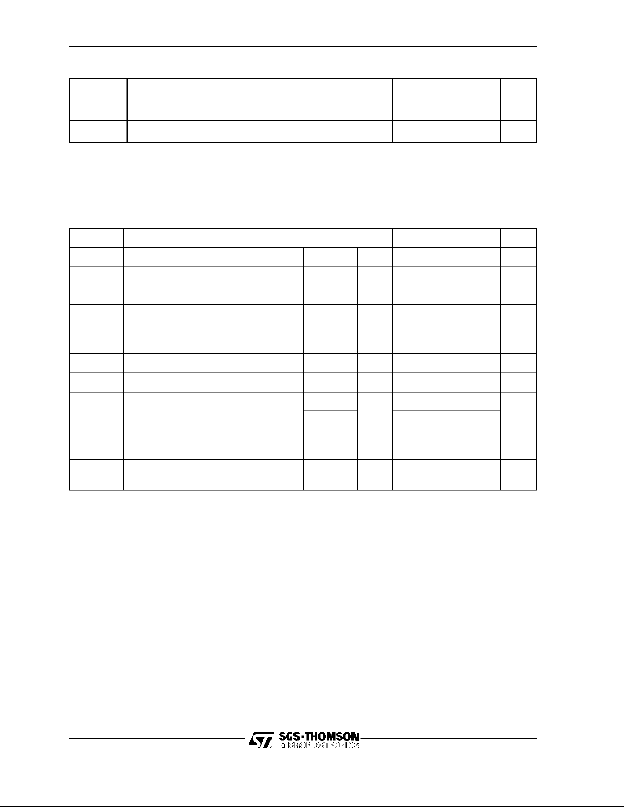
ABSOLUTE RATINGS (limitingvalues)
Symbol Parameter Value Unit
TO220AB
(Plastic)
G
A
K
I
T(RMS)
I
T(AV)
I
TSM
I2tI
I
TM
dI/dt Critical rate of rise of on-state current
Tstg
Tj
Tl Maximum lead temperature for soldering during 10 s at 4.5 mm
Symbol Parameter TYP Unit
RMS on-state current
(180° conduction angle, single phase circuit)
Average on-state current
(180° conduction angle, single phase circuit)
Non repetitive surge peak on-state current
( Tj initial = 25°C)
2
t value tp = 10 ms 450 A2s
Non repetitive surge peak on-state current
( Tj initial = 25°C)
Exponential pulse wave form
Gate supply : IG= 100 mA diG/dt = 1 A/µs
Storage and operating junction temperature range - 40 to + 150
from case
Tc = 110 °C12 A
Tc = 110 °C8 A
tp = 8.3 ms 315 A
tp = 10 ms 300
tp = 1 ms 750 A
100 A/µs
- 40 to + 125
260 °C
212 512 1012 2012
°C
°C
V
DRM
V
RRM
April 1995
Repetitive peak off-state voltage
Tj = 125 °C
25 50 100 200 V
1/5
TYP 212 ---> T Y P 2012
THERMAL RESISTANCES
Symbol Parameter Value Unit
Rth (j-a) Junction to ambient 60 °C/W
Rth (j-c) DC Junction to case for DC 1.3 °C/W
GATE CHARACTERISTICS (maximumvalues)
P
ELECTRICAL CHARACTERISTICS
=1W PGM= 10W (tp = 20 µs) I
G (AV)
Symbol Test Conditions Value Unit
=4A(tp=20µs) V
FGM
RGM
=5V.
I
GT
V
GT
V
GD
tgt VD=V
I
L
I
H
V
TM
I
DRM
I
RRM
dV/dt Linear slope up to VD=67%V
tq VD=67%V
VD=12V (DC) RL=33Ω Tj=25°C MAX 30 mA
VD=12V (DC) RL=33Ω Tj=25°C MAX 1.5 V
VD=V
DRMRL
DRMIG
dIG/dt = 1.5A/µs
IG= 1.2 I
IT= 500mA gate open Tj=25°C MAX 50 mA
ITM= 50A tp= 380µs Tj=25°C MAX 1.5 V
V
DRM
V
RRM
gate open
dITM/dt=30 A/µsdV
=3.3kΩ Tj= 125°C MIN 0.2 V
= 200mA
GT
Rated
Rated
DRMITM
= 50A VR= 25V
/dt= 50V/µs
D
DRM
Tj=25°C TYP 1 µs
Tj=25°C TYP 60 mA
Tj=25°C MAX 0.01 mA
Tj= 125°C2
Tj= 125°C MIN 200 V/µs
Tj= 125°C TYP 100 µs
2/5
 Loading...