

DUAL CMOS RAIL TO RAIL OPERATIONAL AMPLIFIER
.
SINGLESUPPLYOPERATIONFROM
2.7V TO 16V
.
LOW SUPPLYCURRENT: 500µA(VCC= 5V)
.
LATCH - UP IMMUNITY
OPERATIONALAMPLIFIERS
.
RAILTO RAILINPUTAND OUTPUT
.
EXTREMELYLOW INPUT BIAS CURRENT :
1pA typ.
.
1MHzTYPICALGAIN BANDWIDTH PRODUCT
.
SPECIFIEDFOR600Ω OUTPUT LOAD
COMPARATORS
.
PUSH-PULL OUTPUT (no external pull-up resistor required)
.
EXTREMELYLOW INPUT BIAS CURRENT :
1pA typ.
.
EXTREMELYLOW INPUT OFFSET
CURRENT: 1pAtyp.
.
INPUTCOMMON-MODE VOLTAGERANGE INCLUDES GROUND
.
HIGHINPUT IMPEDANCE: 1012typ.
.
FASTRESPONSETIME :2µs TYP. FOR 5mV
OVERDRIVE
.
SPICEMACROMODEL INCLUDED IN THIS
SPECIFICATION
TSM221
AND DUAL CMOS COMPARATOR
N
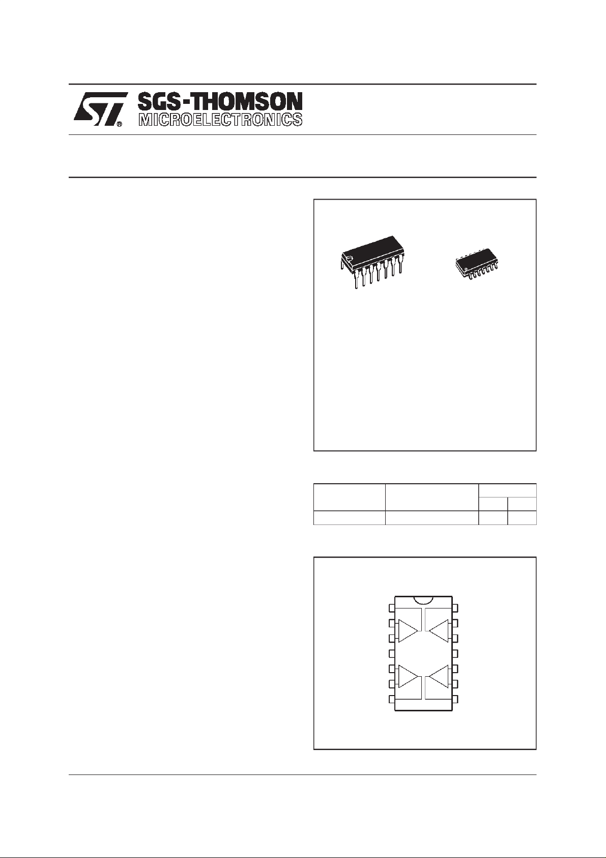
DIP14
(Plastic Package)
ORDER CODES
Part Number Temperature Range
TSM221I -40, +125
(Plastic Micropackage)
D
SO14
Package
o
C ••
ND
DESCRIPTION
The TSM221isa space-savingmonolithicICwhich
includes a dual Rail to Rail op-amp and a micropower dual comparator, using a CMOS process.
Thismixedcircuitisa generalpurposeanalogblock
for Telecom or Industrial applications,offering an
integratedhigh performancessolution.
December 1997
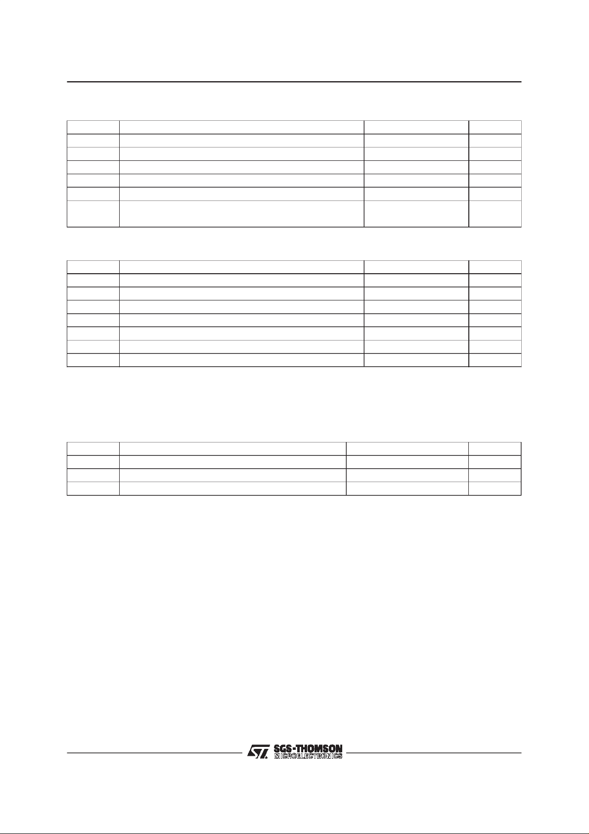
PIN CONNECTIONS (top view)
Output 1
1
Inve rting Input 1
Non-inverting Input 1
Non-inve rting Input 2
Inve rting Input 2
Output2
2
-
+
3
Op-a mp1
+
CCV
4
5
+
-
6
Comp1 Comp2
7
Op-a mp2
-
+
+
-
14
Output 4
Inve rting Input 4
13
Non-inverting Input 4
12
-
CCV
11
Non-inverting Input 3
10
Inve rting Input 3
9
Output 3
8
1/11
TSM221
ABSOLUTEMAXIMUM RATINGS (OPERATIONALAMPLIFIERS)
Symbol Parameter Value Unit
V
CC
V
id
V
I
in
I
o
T
oper
T
stg
ABSOLUTEMAXIMUM RATINGS (COMPARATORS)
Symbol Parameter Value Unit
V
CC
V
id
V
V
O
I
o
T
oper
T
stg
Notes : 1. All voltages values, except differential voltage are with respect to network ground terminal.
Supply Voltage - (note 1) 18 V
Differential Input Voltage -(note 2) ±18 V
Input Voltage - (note3) -0.3 to 18 V
i
Current on Inputs (Op-Amps) ±50 mA
Current on Outputs (Op-Amps) ±130 mA
Operating Free Air Temperature Range -40 to +125
Storage Temperature -65 to +125
Supply Voltage - (note 1) 18 V
Differential Input Voltage -(note 2) ±18 V
Input Voltage - (note4) -0.3 to 18 V
i
Output Voltage 18 V
Output Current (Comparators) 20 mA
Operating Free Air Temperature Range -40 to +125
Storage Temperature -65 to +125
2. Differential voltages are non-inverting input terminal with respect to the inverting input terminal.
3. The magnitude of input and output voltages must never exceed (V
4. The magnitude of input and output voltages must never exceed the magnitude of the positive supply voltage.
+
CC
) +0.3V.
o
C
o
C
o
C
o
C
OPERATING CONDITIONS
Symbol Parameter Value Unit
V
CC
V
icm
V
icm
Supply Voltage 2.7 to 16 V
Common Mode Input Voltage Range (Op-Amps) Vdd-0.2 to VCC+0.2 V
Common Mode Input Voltage Range (Comparators) 0 to V
+
-1.5 V
CC
2/11
TSM221
OPERATIONAL AMPLIFIERS
ELECTRICALCHARACTERISTICS
+
=5V,V
V
CC
Symbol Parameter Test Condition Min. Typ. Max. Unit
V
io
DV
io
I
io
I
ib
A
vd
I
CC
CMR Common Mode Rejection Ratio V
SVR Supply Voltage RejectionRatio V
V
OH
V
OL
I
o
I
sink
GBP Gain Bandwidth Product A
SR Slew Rate A
∅m Phase Margin 30 Degrees
e
n
C
s
Note 1 : Maximum values including unavoidable inaccuracies of the industrial test.
Note 2 : Op-amps and comparators
-
=0V,RL,CLconnectedto VCC/2, T
CC
InputOffset Voltage
≤ T
T
min.
=25oC (unless otherwise specified)
amb
≤ T
amb
max.
10
12
mV
InputOffset Voltage Drift 5 µV/oC
InputOffset Current - (note 1)
≤ T
T
min.
amb
≤ T
max.
InputBias Current - (note 1)
≤ T
T
min.
amb
≤ T
max.
LargeSignal Voltage Gain RL= 10kΩ,VO= 1.5V to 3.5V
≤ T
T
min.
amb
≤ T
max.
10
7
1 100
pA
200
1 150
pA
300
50 V/mV
TotalSupply Current- (note 2) No load 500 800 µA
= 1.5 to 3.5V, Vo= 2.5V 60 85 dB
ic
+
= 3V to 5V,VO=VCC/2 55 80 dB
CC
HighLevel OutputVoltage
R1 connected to V
CC/2
Low Level Output Voltage
R1 connected to V
CC/2
Output Short Circuit Current Vo=V
Output Sink Current Vo=V
RL= 10k
= 600Ω
R
L
= 100Ω
R
L
4.90
4.25
RL= 10k
= 600Ω
R
L
= 100Ω
R
L
-
CC
+
CC
= 100, RL= 10k,
VCL
= 100pF, f = 100kHz 1
C
L
=1,RL= 10k,
VCL
= 100pF, Vi= 1V to 4V 0.7
C
L
45 65 mA
45 65 mA
4.95
4.55
3.7
40
350
1400
100
500
mV
MHz
V/µs
Equivalent Input Noise Voltage Rs= 100Ω, f = 1kHz 30 nV
√Hz
ChannelSeparation f = 1kHz 120 dB
V
3/11
TSM221
OPERATIONALAMPLIFIERS
ELECTRICAL CHARACTERISTICS
+
=3V,V
V
CC
Symbol Parameter Test Condition Min. Typ. Max. Unit
V
io
DV
io
I
io
I
ib
A
vd
I
CC
CMR Common Mode Rejection Ratio V
SVR Supply Voltage Rejection Ratio V
V
OH
V
OL
I
o
I
sink
GBP Gain Bandwidth Product A
SR Slew Rate A
∅m Phase Margin 30 Degrees
e
n
C
s
Note 1 : Maximum values including unavoidable inaccuracies of the industrialtest.
Note 2 : Op-amps and comparators
-
=0V,RL,CLconnectedto VCC/2, T
CC
Input Offset Voltage
≤ T
T
min.
amb
=25oC(unless otherwise specified)
amb
≤ T
max.
10
12
Input Offset Voltage Drift 5 µV/oC
Input Offset Current - (note1)
≤ T
T
min.
amb
≤ T
max.
Input Bias Current - (note 1)
≤ T
T
min.
amb
≤ T
max.
Large Signal Voltage Gain RL= 10kΩ,VO= 1.5V to 3.5V
≤ T
T
min.
amb
≤ T
max.
3
2
1 100
200
1 150
300
10 V/mV
Total Supply Current- (note2) No load 415 600 µA
= 0 to 3V, Vo= 1.5V 70 dB
ic
+
= 2.7V to 3.3V, VO=VCC/2 50 80 dB
CC
High Level Output Voltage
R1 connected to V
CC/2
Low Level Output Voltage
R1 connected to V
CC/2
Output Short Circuit Current Vo=V
Output Sink Current Vo=V
RL= 10k
= 600Ω
R
L
= 100Ω
R
L
2.90
2.30
RL= 10k
= 600Ω
R
L
= 100Ω
R
L
-
CC
+
CC
= 100, RL= 10k,
VCL
= 100pF, f = 100kHz 0.8
C
L
=1,RL= 10k,
VCL
= 100pF, Vi= 1.3V to 1.7V 0.3
C
L
20 40 mA
20 40 mA
2.96
2.60
2
30
300
900
70
400
MHz
V/µs
Equivalent Input Noise Voltage Rs= 100Ω, f = 1kHz 30 nV
√Hz
Channel Separation f = 1kHz 120 dB
mV
pA
pA
V
mV
4/11

MACROMODEL FOR OP-AMPS (VCC= 3V)
Applies to : TSM221
TSM221
** Standard Linear Ics Macromodels,1993.
** CONNECTIONS :
* 1 INVERTING INPUT
* 2 NON-INVERTING INPUT
* 3 OUTPUT
* 4 POSITIVEPOWER SUPPLY
* 5 NEGATIVE POWER SUPPLY
.SUBCKT TSM2213V 1 3 2 4 5 (analog)
**********************************************************
.MODEL MDTH D IS=1E-8 KF=6.564344E-14CJO=10F
* INPUT STAGE
CIP 2 5 1.000000E-12
CIN 1 5 1.000000E-12
EIP 10 52 51
EIN 16 5 1 5 1
RIP 10 11 6.500000E+00
RIN 15 16 6.500000E+00
RIS 11 15 1.271505E+01
DIP 11 12 MDTH 400E-12
DIN 15 14 MDTH 400E-12
VOFP 12 13 DC 0.000000E+00
VOFN 13 14 DC 0
IPOL 13 54.000000E-05
CPS 11 15 2.125860E-08
DINN 17 13 MDTH 400E-12
VIN 17 5 0.000000e+00
DINR 15 18 MDTH 400E-12
VIP 4 18 0.000000E+00
FCP 4 5 VOFP 5.000000E+00
FCN 5 4 VOFN 5.000000E+00
* AMPLIFYING STAGE
FIP 5 19 VOFP 2.750000E+02
FIN 5 19 VOFN 2.750000E+02
RG1 19 5 1.916825E+05
RG2 19 4 1.916825E+05
CC 19 29 2.200000E-08
HZTP 30 29 VOFP 1.3E+03
HZTN 5 30 VOFN 1.3E+03
DOPM 19 22MDTH 400E-12
DONM 21 19 MDTH 400E-12
HOPM 22 28 VOUT 3800
VIPM 28 4150
HONM 21 27 VOUT 3800
VINM 5 27 150
EOUT 26 23 195 1
VOUT 23 50
ROUT 26 3 75
COUT 3 51.000000E-12
DOP 19 68MDTH 400E-12
VOP 4 25 1.724
HSCP 68 25 VSCP1 0.8E8
DON 69 19MDTH 400E-12
VON 24 5 1.7419107
HSCN 24 69 VSCN1 0.8E+08
VSCTHP 60 610.0875
** VSCTHP = leseuil au dessus de vio * 500
** c.a.d 275U-000Udus a l’offset
DSCP1 61 63MDTH 400E-12
VSCP1 63 640
ISCP 64 0 1.000000E-8
DSCP2 0 64 MDTH 400E-12
DSCN2 0 74 MDTH 400E-12
ISCN 74 01.000000E-8
VSCN1 73 74 0
DSCN1 71 73 MDTH 400E-12
VSCTHN 71 70 -0.55
** VSCTHN = le seuil audessous de vio * 2000
** c.a.d -375U-000Udus a l’offset
ESCP 60 0 2 1 500
ESCN 70 02 1 -2000
.ENDS
ELECTRICAL CHARACTERISTICS V
CC
+
= 3V, V
-
= 0V,RL,CLconnectedto VCC/2, T
CC
amb
unless otherwise specified
Symbol Conditions Value Unit
V
io
A
vd
I
CC
V
icm
V
OH
V
OL
I
sink
I
source
RL= 10kΩ 10 V/mV
No load 415 µA
RL= 10kΩ 2.96 V
RL= 10kΩ 30 mV
VO=3V 40 mA
VO=0V 40 mA
GBP R
SR R
= 10k
L
= 10k
L
Ω,
CL= 100pF 0.8 MHz
Ω,
CL= 100pF 0.3 V/µs
0mV
-0.2 to 3.2 V
=25oC,
5/11

TSM221
MACROMODEL FOR OP-AMPS (VCC= 5V)
Applies to : TSM221
** Standard Linear Ics Macromodels,1993.
** CONNECTIONS :
* 1 INVERTING INPUT
* 2 NON-INVERTING INPUT
* 3 OUTPUT
* 4 POSITIVEPOWER SUPPLY
* 5 NEGATIVE POWER SUPPLY
* 6 STANDBY
.SUBCKT TSM2215V 1 3 2 4 5 (analog)
**********************************************************
.MODEL MDTH D IS=1E-8 KF=6.564344E-14CJO=10F
* INPUT STAGE
CIP 2 5 1.000000E-12
CIN 1 5 1.000000E-12
EIP 10 52 51
EIN 16 5 1 5 1
RIP 10 11 6.500000E+00
RIN 15 16 6.500000E+00
RIS 11 15 7.322092E+00
DIP 11 12 MDTH 400E-12
DIN 15 14 MDTH 400E-12
VOFP 12 13 DC 0.000000E+00
VOFN 13 14 DC 0
IPOL 13 54.000000E-05
CPS 11 15 2.498970E-08
DINN 17 13 MDTH 400E-12
VIN 17 5 0.000000e+00
DINR 15 18 MDTH 400E-12
VIP 4 18 0.000000E+00
FCP 4 5 VOFP 5.750000E+00
FCN 5 4 VOFN 5.750000E+00
ISTB0 5 4 500N
* AMPLIFYING STAGE
FIP 5 19 VOFP 4.400000E+02
FIN 5 19 VOFN 4.400000E+02
RG1 19 5 4.904961E+05
RG2 19 4 4.904961E+05
CC 19 29 2.200000E-08
HZTP 30 29 VOFP 1.8E+03
HZTN 5 30 VOFN 1.8E+03
DOPM 19 22MDTH 400E-12
DONM 21 19 MDTH 400E-12
HOPM 22 28 VOUT 3800
VIPM 28 4230
HONM 21 27 VOUT 3800
VINM 5 27 230
EOUT 26 23 195 1
VOUT 23 50
ROUT 26 3 82
COUT 3 51.000000E-12
DOP 19 68MDTH 400E-12
VOP 4 25 1.724
HSCP 68 25 VSCP1 0.8E+08
DON 69 19MDTH 400E-12
VON 24 5 1.7419107
HSCN 24 69 VSCN1 0.8E+08
VSCTHP 60 610.0875
** VSCTHP = leseuil au dessus de vio * 500
** c.a.d 275U-000Udus a l’offset
DSCP1 61 63MDTH 400E-12
VSCP1 63 640
ISCP 64 0 1.000000E-8
DSCP2 0 64 MDTH 400E-12
DSCN2 0 74 MDTH 400E-12
ISCN 74 01.000000E-8
VSCN1 73 74 0
DSCN1 71 73 MDTH 400E-12
VSCTHN 71 70 -0.55
** VSCTHN = le seuil audessous de vio * 2000
** c.a.d -375U-000Udus a l’offset
ESCP 60 0 2 1 500
ESCN 70 02 1 -2000
.ENDS
ELECTRICAL CHARACTERISTICS V
CC
+
= 5V, V
-
= 0V,RL,CLconnectedto VCC/2, T
CC
unless otherwise specified
Symbol Conditions Value Unit
0mV
-0.2 to 5.2 V
A
I
V
V
V
I
I
source
GBP R
SR R
6/11
V
CC
sink
icm
OH
OL
io
vd
RL= 10kΩ 50 V/mV
No load 500 µA
RL= 10kΩ 4.95 V
RL= 10kΩ 40 mV
VO=5V 65 mA
VO=0V 65 mA
= 10k
Ω,
L
= 10k
L
CL= 100pF 1 MHz
Ω,
CL= 100pF 0.7 V/µs
amb
=25oC,

TSM221
COMPARATORS
ELECTRICAL CHARACTERISTICS
+
=5V,V
V
CC
Symbol Parameter Test Condition Min. Typ. Max. Unit
V
io
I
io
I
ib
V
OH
V
OL
V
icm
CMR Common Mode Rejection Ratio V
SVR Supply Voltage Rejection Ratio V
T
plh
T
ph1
T
f
T
R
Note 1 : The specified offset voltageis the maximum value required todrive the output up to 4.5V or down to 0.3V.
Note 2 : Maximum values including unavoidable inaccuracies of the industrialtest.
-
=0V,T
CC
Input Offset Voltage - (note 1)
≤ T
T
min.
amb
=25oC (unless otherwise specified)
amb
Vic=V
icm min.
≤ T
max.
+
V
CC
= 5V to 10V
Input Offset Current - (note2)
≤ T
T
min.
amb
≤ T
max.
Input Bias Current - (note 2)
≤ T
≤ T
≤ T
amb
amb
amb
≤ T
≤ T
≤ T
max.
max.
max.
Vid= 1V,
= -4mA
I
oh
Vid= -1V,
= 4mA
I
oh
T
min.
High Level Output Voltage
T
min.
Low Level Output Voltage
T
min.
Input Common Mode Voltage
≤ T
T
min.
Response Time Low to High
Overdrive = 5mV
Overdrive = 10mV
amb
≤ T
max.
ic=Vicm min.
+
= 5V to 10V 90 dB
CC
= 0V, f = 10kHz,
V
ic
= 50pF 1.5
C
L
Overdrive = 20mV
Overdrive = 40mV
TTL input
Response Time High to Low
Overdrive = 5mV
Overdrive = 10mV
= 0V, f = 10kHz,
V
ic
= 50pF 2.2
C
L
Overdrive = 20mV
Overdrive = 40mV
TTL input
Fall Time f = 10kHz, CL= 50pF,
overdrive50mV
Rise Time f = 10kHz, CL = 50pF,
overdrive50mV
0toV
0toV
4.5
4.3
CC
CC
1.1
0.9
0.7
0.6
1.6
1.1
0.75
0.17
+
+
-1.2
-1.5
5
6.5
1
300
1
600
4.7 V
220 300
375
82 dB
30 ns
30 ns
mV
pA
pA
mV
µs
µs
7/11

TSM221
COMPARATORS
ELECTRICAL CHARACTERISTICS
+
=3V,V
V
CC
Symbol Parameter Test Condition Min. Typ. Max. Unit
V
io
I
io
I
ib
V
OH
V
OL
V
icm
CMR Common Mode Rejection Ratio V
SVR Supply Voltage Rejection Ratio V
T
plh
T
phl
T
f
T
R
Note 1 : The specified offset voltageis the maximum value required todrive the output up to 4.5V or down to 0.3V.
Note 2 : Maximum values including unavoidable inaccuracies of the industrialtest.
-
=0V,T
CC
Input Offset Voltage - (note 1)
≤ T
T
min.
amb
=25oC (unless otherwise specified)
amb
Vic= 1.5V 5
≤ T
max.
Input Offset Current - (note2)
≤ T
T
min.
amb
≤ T
max.
Input Bias Current - (note 2)
≤ T
≤ T
≤ T
amb
amb
amb
≤ T
≤ T
≤ T
max.
max.
max.
Vid= 1V,
= -4mA
I
oh
Vid= -1V,
= 4mA
I
oh
T
min.
High Level Output Voltage
T
min.
Low Level Output Voltage
T
min.
Input Common Mode Voltage
≤ T
T
min.
Response Time Low to High
Overdrive = 5mV
TTL input
Response Time High to Low
Overdrive = 5mV
TTL input
amb
≤ T
max.
ic=Vicm min.
+
= 5V to 10V 75 dB
CC
= 0V, f = 10kHz,
V
ic
= 50pF 1.5
C
L
= 0V, f = 10kHz,
V
ic
= 50pF 2.2
C
L
Fall Time f = 10kHz, CL= 50pF,
overdrive50mV
Rise Time f = 10kHz, CL = 50pF,
overdrive50mV
0toV
0toV
2
1.8
CC
CC
0.7
0.15
+
+
6.5
1
300
1
600
2.4 V
300 400
450
-1.2
-1.5
80 dB
30 ns
30 ns
mV
pA
pA
mV
µs
µs
8/11

MACROMODEL FOR COMPARTORS (VCC= 3V)
Applies to : TSM221
TSM221
** Standard Linear Ics Macromodels,1993.
** CONNECTIONS :
* 1 INVERTING INPUT
* 2 NON-INVERTING INPUT
* 3 OUTPUT
* 4 POSITIVEPOWER SUPPLY
* 5 NEGATIVE POWER SUPPLY
.SUBCKT TSM221C 1 3 2 4 5
**********************************************************
************************* RVAR *************************
.SUBCKT RVAR 20 10 IN OUT
VSENS0 IN 1 0V
R0 1 OUT 125
F0 1 OUT POLY(2) VSENS0 VSENS2 0 0 0 0 1E+08
VSENS2 20 3 0V
R2 3 10 1E+09
.ENDS RVAR
*********************** COMPARATOR *********************
.MODEL MDTH D IS=1E-11 KF=1.050321E-32
CJO=10F
* INPUT STAGE
CIP 2 5 1.000000E-12
CIN 1 5 1.000000E-12
EIP 10 02 01
EIN 16 0 1 0 1
RIP 10 11 6.500000E+01
RIN 15 16 6.500000E+01
RIS 11 15 1.939046E+02
DIP 11 12 MDTH 400E-12
DIN 15 14 MDTH 400E-12
VOFP 12 13 DC 0.000000E+00
VOFN 13 14 DC 0
IPOL 13 0100E-06
CPS 11 15 8.16E-09
DINN 17 13 MDTH 400E-12
VIN 17 5 0.000000e+00
DINR 15 18 MDTH 400E-12
VIP 4 18 1.200000E+00
FCP 4 5 VOFP 0.02
FCN 5 4 VOFN 0.02
FIBP 2 0 VOFN 2.000000E-08
FIBN 0 1 VOFP2.000000E-08
* AMPLIFYING STAGE
RG1 5 19 2.8E+05
RG2 4 19 2.8E+05
DOPM 19 22MDTH 400E-12
DONM 21 19 MDTH 400E-12
HOPM 22 28 VOUT 3000
VIPM0 28 40-87
EIPM 40 44 5 42
**VIPM 28 4 150
HONM 21 27 VOUT 3000
VINM0 50 27 -114
EINM 5 50 4 5 54
**VINM 5 27 150
DOP 19 25MDTH 400E-12
VOP 4 25 1.097
DON 24 19MDTH 400E-12
VON 24 5 1.097
FIP 0 19 VOFP 104
FIN 0 19 VOFN 104
EOUT 26 23 195 1
VOUT 23 5 0V
XOUT 4 5 26 3 RVAR
*ROUT 26 3 62.5
.ENDS
ELECTRICAL CHARACTERISTICS V
CC
+
= 3V, V
CC
-
= 0V,T
=25oC, unless otherwise specified
amb
Symbol Conditions Value Unit
Vic= 1.5V 0 mV
No load, peroperator 7 µA
0to1.8V V
Vid= 1V, IOH= -4mA 2.4 V
Vid= 1V, IOH= -4mA 300 mV
Overdrive = 5mV 1.5 µs
Overdrive = 5mV 2.2 µs
V
V
V
t
t
V
I
CC
PLH
PHL
io
icm
OH
OL
9/11

TSM221
PACKAGE MECHANICALDATA
14 PINS- PLASTICDIP
Dim.
a1 0.51 0.020
B 1.39 1.65 0.055 0.065
b 0.5 0.020
b1 0.25 0.010
D 20 0.787
E 8.5 0.335
e 2.54 0.100
e3 15.24 0.600
F 7.1 0.280
i 5.1 0.201
L 3.3 0.130
Z 1.27 2.54 0.050 0.100
Min. Typ. Max. Min. Typ. Max.
Millimeters Inches
10/11

PACKAGE MECHANICALDATA
14 PINS - PLASTICMICROPACKAGE(SO)
TSM221
Dim.
Min. Typ. Max. Min. Typ. Max.
Millimeters Inches
A 1.75 0.069
a1 0.1 0.2 0.004 0.008
a2 1.6 0.063
b 0.35 0.46 0.014 0.018
b1 0.19 0.25 0.007 0.010
C 0.5 0.020
c1 45
o
(typ.)
D 8.55 8.75 0.336 0.334
E 5.8 6.2 0.228 0.244
e 1.27 0.050
e3 7.62 0.300
F 3.8 4.0 0.150 0.157
G 4.6 5.3 0.181 0.208
L 0.5 1.27 0.020 0.050
M 0.68 0.027
S8
Information furnished is believed to be accurate and reliable. However, SGS-THOMSON Microelectronics assumes no responsibility
for the consequences of use of suchinformation nor for any infringement of patents or other rights of third parties which may result
from its use. No license is granted by implication or otherwise under any patent or patent rights of SGS-THOMSON Microelectronics.
Specification mentioned in this publication are subject to change without notice. This publication supersedes and replaces all
information previously supplied. SGS-THOMSON Microelectronics products are not authorized for use as critical components in life
support devices or systems without express written approval of SGS-THOMSON Microelectronics.
o
(max.)
1997 SGS-THOMSON Microelectronics – Printed in Italy – AllRights Reserved
SGS-THOMSONMicroelectronics GROUP OF COMPANIES
Australia- Brazil - Canada - China - France - Germany - Italy - Japan - Korea - Malaysia - Malta - Morocco
The Netherlands - Singapore - Spain - Sweden - Switzerland - Taiwan- Thailand -United Kingdom - U.S.A.
ORDER CODE :
11/11
 Loading...