

1/7
■ OVER VOLTAGE PROTECTION FOR 3.3V
5V AND 12V WITHOUT EXTERNAL COMPONENTS
■ UNDER VOLTAGE PROTECTION FOR 3.3V
5V AND 12V WITHOUT EXTERNAL COMPONENTS
■ OVER VOLTAGE PROTECTION FOR -12V
OR -5V W I T H EX TERNAL COMPON E N TS
■ EXTERNALLY ADJUSTABLE UNDER VOLT-
AGE BLANKING DURING POWER UP
■ POWER GOOD I N PUT / OU TP U T
■ EXTERNALLY ADJUSTABLE PG DELAY
■ F AULT OUTPUT
■ REMOTE OUTPUT
■ EXTERNALLY ADJUSTABLE REMOTE
DELAY
■ PRECISION VOLTAGE REFERENCE
■ 2kV ESD PROTECTION
DESCRIPTION
The TSM112 integrated circuit incorporates all
sensing circuitry to regulate and protect from over
voltage and under voltage a multiple output power
supply (3.3V, 5V and 12V).
TSM112 incorporat es all the nec essary functions
for Housekeeping features whi ch allow s afe operation in all conditions, and very hi gh system integration.
TSM112 integrates a precise voltage reference.
APPLICATION
■ PC SMPS Triple Power Line Housekeeping
IC (3.3V 5V 12V)
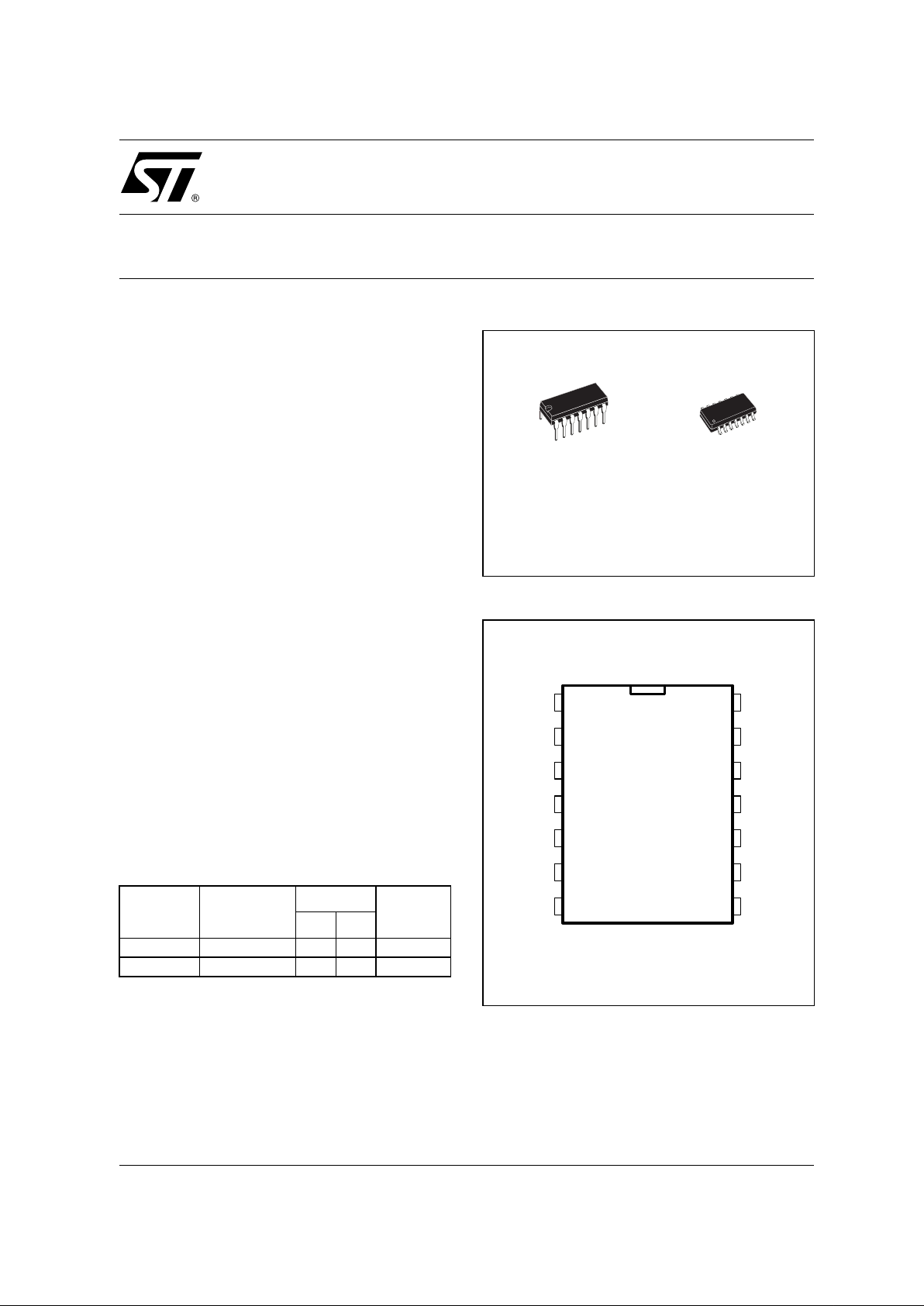
ORDER CODE
N = Dual in Line Package (DIP)
D = Small Outline Package (SO) - also available in Tape & Reel (DT)
PIN CONNECTIONS (top view)
Part
Number
Temperature
Range
Package
Marking
ND
TSM112CN 0 to 85°C
•
TSM112C
TSM112CD 0 to 85°C
•
M112
N
DIP14
(Plastic Package)
D
SO14
(Plastic Micropackage)
VCC
REM
TREM
TPG
PG
VS33
VS5
VS12
PI
TUV
EP
GND VREF
10
9
87
6
5
4
3
2
1
11
12
1314FAUL
T
January 2001
TSM112
3.3V 5V 12V HOUSEKEEPING IC
TSM112
2/7
PIN DESCRIPTION
ABSOLUTE MAXIMUM RATINGS
OPERATING CONDITIONS
Name Pin # Type Function
Vcc 14 Power Supply Positive Power Supply Line
Gnd 7 Power Supply Ground Line. 0V Reference For All Voltages
Vs12 3 Analog Input
Over and Under voltage Sense Input Dedicated to the 12V Line
1)
Vs5 2 Analog Input
Over and Under voltage Sense Input Dedicated to the 5V Line
1)
Vs33 1 Analog Input
Over and Under voltage Sense Input Dedicated to the 3.3V Line
1)
Tuv 6 Timing Capacitor Adjustable Under voltage Blanking Delay at Power Up (Setting Capacitor)
Fault 13 Open Collector Fault Output. Fault is high when Over or Under Voltage has been Detected
PI 5 Analog Input Power Good Input. Detection of the Power Conditions
PG 12 Open Collector Power Good Output. PG output is High when the Power Conditions are
OK
Tpg 11 Timing Capacitor Adjustable Power Good Delay (Setting Capacitor)
REM 9 Logic Input Input Remote Control of the Complete System by the Motherboard
(µController). Remote is active high. Switch OFF/ON of the Power Supply.
Reset of the Complete System after a FAULT Activation.
Trem 10 Timing Capacitor Adjustable Remote Delay (Setting Capacitor).
Vref 8 Voltage Reference 2.5V Reference for all Voltages
EP 4 Analog Input Extra Protection Circuit. Can be used for -12V or -5V Over Voltage
Protection.
1. Over and Under Voltage Inputs can go higher than Vcc within the allowed Max Rating range
Symbol DC Supply Voltage Value Unit
Vcc
DC Supply Voltage
1)
25 V
Iout Output Current Power Good 30 mA
Io Output current for the Voltage reference 20 mA
VFault Fault Ouput 5 V
Top Operating Free Air Temperature Range -55 to 125 °C
Pd Power Dissipation 0.7 W
Tstg Storage Temperature -55 to 150 °C
ESD Electrostatic Discharge 2 kV
Tuv Adjustable Under voltage Blanking At Power UP 5 V
EP Extra Protection 5 V
PI Power Good Input 5 V
PG Power Good Output 5 V
Tpg Adjustable Power Good Delay 5 V
REM Remote Control 5 V
Trem Adjustable Remote Delay 5 V
1. All voltage values, except differential voltage are with respect to network ground terminal.
Symbol Parameter Value Unit
Vcc DC Supply Conditions 4.5 to 24 V
Toper Operating Free Air Temperature Range 0 to 85 °C
TSM112
3/7
ELECTRICAL CHARACTERISTICS
Tamb = 25°C and Vcc = 17V (unless otherwise specified)
Symbol Parameter Test Condition Min Typ Max Unit
Total Current Consumption
Icc Total Supply Current 3 5 mA
Over Voltage and Under Voltage Protection
Vov33 Over Voltage Sense 3.3V Input can go higher than
Vcc
3.8 4 4.2 V
Vov5 Over Voltage Sense 5V Input can go higher than
Vcc
5.8 6.1 6.4 V
Vov12 Over Voltage Sense12V Input can go higher than
Vcc
13.4 14.2 15 V
Vuv33 Under Voltage Sense 3.3V 2.1 2.3 2.5 V
Vuv5 Under Voltage Sense 5V 3.7 4 4.3 V
Vuv12 Under Voltage Sense 12V 9.2 10 10.8 V
Vep Extra Over voltage Protection Threshold 1.28 V
Tfault Fault Delay Before Latching Internally Fixed Delay 100
µ
s
Under Voltage Blanking During Power Up
Tuv Under Voltage Blanking During Power
Up (Vcc rising)
Cuv = 2.2µF
Adjustable Blanking
100 300 500 ms
Thuv Blanking Threshold 1.28 V
Power Good (PG)
Vpgth Power Good Voltage Threshold 1.28 V
Vpghyst Power Good Voltage Threshold
Hysteresis
70 mV
Vpgol Low Output Open Collector Saturation
Voltage
Collector Current = 15mA 0.4 V
Ipgoh High Output Open Collector Leakage
Current
PG Output = 5V 1
µ
A
Tpgr Power Good Output Rise Time Load Capacitor = 100pF 1
µ
s
Tpgf Power Good Output Fall Time Load Capacitor = 100pF 1
µ
s
Tpg Power Good Adjustable Delay Load Capacitor Cpg=2.2µF 100 300 500 ms
PIth Power Input Detection Threshold 1.28 V
Fault
Vfaultol Fault Output Saturation Voltage Level IFault = 1mA 1 V
Ifaultoh Fault Output Leakage Current Level Vfault = 5V 1 µA
Remote Control (REM)
Vremth Remote ON/OFF Input Voltage
Threshold
0.7 0.8 1 V
Vremih High Input Remote Voltage 3.3 3.4 V
Iremil Low Input Remote Saturation Current 0.5 mA
Trem1 Remote Adjustable Delay ON to OFF Load Capacitor
Crem=0.1µF
40 50 60 ms
Trem2 Remote Adjustable Delay OFF to ON Load Capacitor
Crem=0.1µF
40 50 60 ms
Voltage Refer ence
Vref Internal Voltage Reference Io = 0mA 2.46 2.5 2.54 V
Regline Line regulation Io = 0mA
4.5V<Vcc<24V
410mV
Regline Line regulation Io = 10mA
4.5V<Vcc<24V
15 mV
Regload
Load regulation
1)
0<Io<10mA 25 mV
1. Do not short circuit the Vref Pin
TSM112
4/7
Figure 1 : Figure 1: Application Sche mat ic
Figure 2 : Internal Schematic
PRIMARY
RECT.
MAIN
CONV.
12V
5V
3.3V
AUX.
CONV.
5Vstby
Vcc
~
TSM112
Over & Undervoltage Protection
Reference
Logic
Sequencer
12V
5V
3.3V
5Vstby
PG
REM
FAULT
PWM + OPTO
PWM + OPTO
+ Vref
+ Vref
OVP
Vref
HOUSEKEEPING
LOGIC
SECONDARY
Vcc
Vs12
Vs5
Vs33
PG
REM
to MOTHERBOARD
FROM
MAIN
CONV.
POWER
SUPPLY
OUTPUT
12V
5V
3.3V
12V
5V
3.3V
PI
TO
UVP
Trem
Tpg
UV
BLANK
Tuv
FAULT
Gnd
TSM112
Vref
Ep
TSM112
5/7
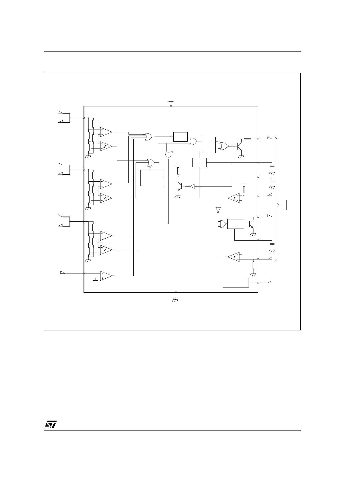
Figure 3 : Figure 3 : Detailed Internal Schematic
Vref
OVP
Vov12
VS12
VS5
VS33
0.8V
FAULT
Rem
Pg
3.47V
SRQ
Vcc
1.25V
PI
VREF
IN 12V
OUT 12V
IN 5V
OUT 5V
IN 3.3V
OUT 3.3V
TO MOTHERBOARD
UVP
Vuv12
Tfault
Tpg
Tpg
Cpg
Trem
Cuv
Tuv
Vref
OVP
Vov5
UVP
Vuv5
Vref
OVP
Vov33
UVP
Vuv33
OVP
UVP
TSM112
Crem
Trem
Tuv
Vcc
Power Up
UV blanking
Gnd
Vref
1.25V
OVP
EP
1k

6/7
TSM112: Housekeeping IC.
TSM112 is a one chip solution for all PC SMPS: it
integrates on one chip the Housekeeping Circuitry
(Over Voltage and Under Voltage protections, with
adequate sequencing).
Triple Power Line Protection.
The TSM112 Housekeeping Circuit is dedicated to
3.3V, 5V and 12V power lines protection. It integrates a Precision Voltage Reference, a Triple
Over Voltage Protection Circuit and a Triple Under
Voltage Protection Circuit as well as all the necessary logic and transient timing management circuits for optimal and secure communication with
the motherboard, du ring start up, switch off and
stabilized conditions.
Over Voltage Protection
The Over Voltage Protection Circuit is made of
three comparators with internal voltage thresholds
(Vov33, Vov5, Vov12) which do not require any
external components for proper operation. The
outputs of these three comparators are ORed.
Under Voltage Protection
The Under Voltage Protection Circuit is made of
three comparators with internal voltage thresholds
(Vuv33, Vuv5, Vuv12) which do not require any
external components for proper operation. The
outputs of these three comparators are ORed, and
blanked by an internal delay circuitry (Power Up
Blanking - Tuv) which can be adjusted with an external capacitor (Cuv). This allows that during
power up, the under voltage protection circuit is inhibited.
Latch OFF
The Over Voltage and Under Voltage Circuits outputs are again ORed before activating a latch.
When activated, this latch commands the full
switch OFF of the three main power lines (3.3V,
5V, 12V) by an ex ternal link between the housekeeping and the primary PWM circuits via the
main optocoupler or any other device . Note that
the Under Voltage Circuit, after Power Up UV
blanking, bears no other delay to the latch setting
input whereas the Over Voltage circuit bears an
additional Tfault delay time. This allows an efficient protection against Output Short Circuit c onditions.
Power Good
The Over Voltage and Under Voltage Circuits are
Ored to switch the Power Good output active (PG)
to warn the motherboard that the voltage of at
least one of the three power li nes is out of range.
The PG activation bears an internal Tpg delay circuitry which can be adjusted with an ex ternal capacitor (Cpg).
Remote Control
Thanks to this information link to the motherboard,
a resetting signal to the latch is achievable with
the Remote pin (REM). When the Remote pin is
active, the external Fault link between Housekeeping circuit and the PWM generator is active
(high = PWM OFF) and the PG pin is active (high).
Note that to reset effectively the latch, a minimum
width Remote pulse should be app lied thanks to
an internal delay circuitry (Trem) which can be adjusted with an external capacitor (Crem).
TSM112
PRINCIPLE OF OPERATION AND APPLICATION HINTS
TSM112
7/7
Information furnished is believed to be accurate and reliable. However, STMicroelectronics assumes no responsibility for the consequences
of use of su ch i n for mat i on n or f or a ny in fr ing em ent o f pa te nts or ot her r igh ts of th ir d pa r tie s w hic h may res ul t f rom i ts us e. No license is granted
by impl i cation or othe rwise under any patent or patent rights of STMicroelectronics. Specificati ons mentione d i n t hi s publication are subject
to change without notice. Thi s publication supersedes and replaces all informat i on previously supplied. STMicr oel ectronics pro ducts are not
authori zed for use as critical components i n l i fe support devices or systems without express w ritten approva l of ST M i croelectronics.
© The ST logo is a registered trademark of STMicroelectronics
© 2001 STMicroelectronics - Printed in Italy - All Rights Reserved
STMicr oelectronics GROUP OF COMPANIE S
Australi a - Brazil - China - F i nl and - France - Ger m any - Hong Kong - I ndi a - Italy - Japan - Ma l aysia - Malta - Mo rocco
Singapo re - Spain - Sweden - Switzerland - United Kingdom
© http://www.st.com
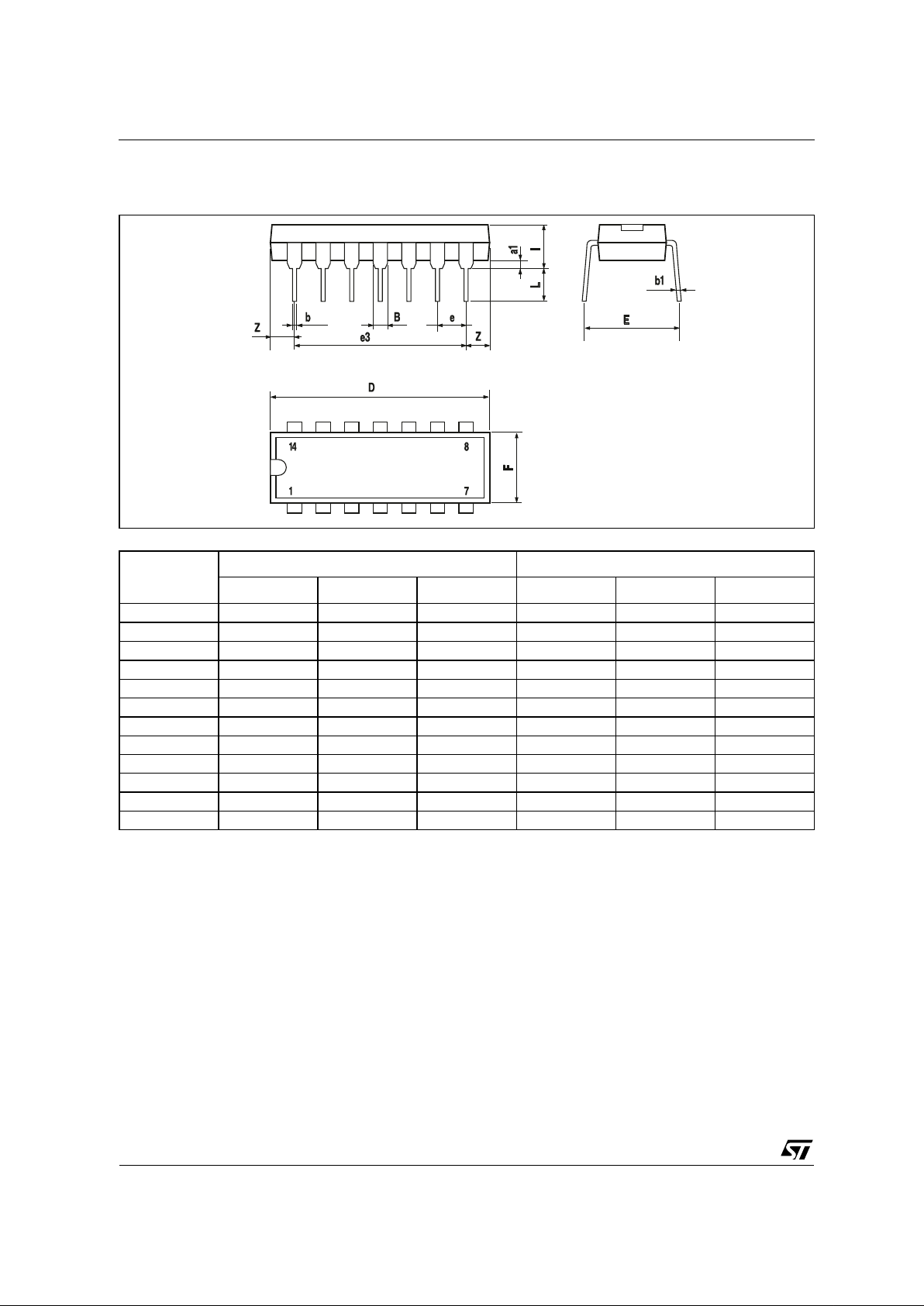
PACKAGE MECHANICAL DATA
14 PINS - PLASTIC PACKAGE
Dim.
Millimeters Inches
Min. Typ. Max. Min. Typ. Max.
a1 0.51 0.020
B 1.39 1.65 0.055 0.065
b 0.5 0.020
b1 0.25 0.010
D 20 0.787
E 8.5 0.335
e 2.54 0.100
e3 15.24 0.600
F 7.1 0.280
i 5.1 0.201
L 3.3 0.130
Z 1.27 2.54 0.050 0.100
 Loading...