

TRIPLEVOLTAGE AND CURRENTSUPERVISOR
.OVERVOLTAGE PROTECTIONFOR 3.3V, 5V
AND 12V WITHOUT EXTERNAL
COMPONENTS
.OVERCURRENT PROTECTION FOR3.3V, 5V
AND 12V WITH INTERNAL THRESHOLD
VOLTAGE
.POWERGOODCIRCUITRY
.GENERATESPOWERGOODSIGNAL
.REMOTE ON/OFFFUNCTION
.PROGRAMMABLE TIMING FOR POWER
GOODSIGNAL
.14.5VTO 36V SUPPLYVOLTAGERANGE
.TWO 1.6% VOLTAGE REFERENCES FOR
MAIN AND AUXILIARY CONVERTER
REGULATIONLOOPS
TSM11 1
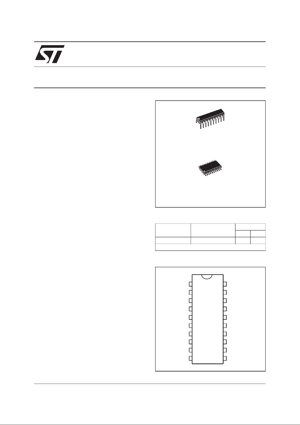
N
DIP20
(Plastic Package)
D
SO20
(PlasticMicropackage)
DESC RIP TI ON
The TSM111 integrated circuit incorporates all
sensingcircuit to control a tripleoutputpower supply.Itincludesvoltagereferences, comparatorsand
matchedresistorsbridge for overcurrentand overvoltage detectionwithout the need of any external
components.Timinggeneratorwithexternalcapacitors, control turn On and Off delays. It providesan
integratedandcost effective solutionforsimultaneous multiple voltagecontrol.
APPL ICATIONS
ThiscircuitisdesignedtobeusedinSMPSforDesktop PC,tosupervisecurrentsandvoltagesof alloutputs and generate power good information to the
system while managing all timing during transitory
operation.
The IC also manages the standbymode of SMPS
while the PCis in sleepmode.
ORDER CODES
Part
Number
TSM111C 0, +70
Example : TSM111CD
PIN CONNE CTIONS (top view)
Vs33
Vs5
Vs12
ADJ
Vcc
PWM
REM
Trem
PG
Tpor
Temperature
Range
1
2
3
4
5
6
7
8
9
10 11
o
C ••
20
Is33
19
Is5
18
Is12
17
Tsur
16
GND
15
FbMAIN
14
VrefMAIN
13
VrefAUX
12
FbAUX
UV
Package
ND
May 1999
1/18
TSM111
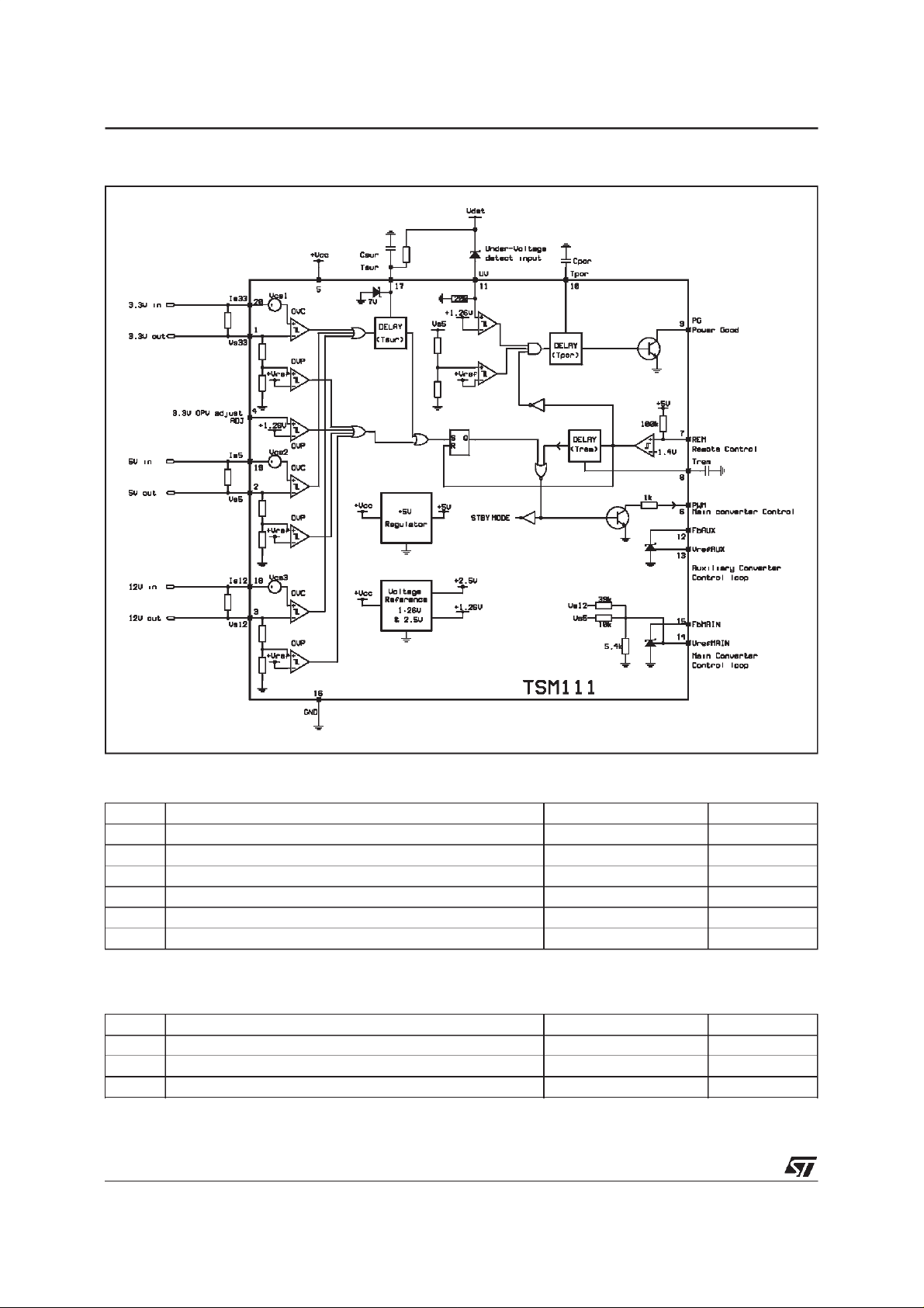
SCHE MATIC DIAGRAM
ABSOLUTE MAXIMUMRATINGS
Symbol Parameter Value Unit
V
I
T
DC Supply Voltage pin 5 - note 1 44 V
CC
Output Current Power Good and PWM 30 mA
out
Power Dissipation 1 W
P
d
Storage Temperature Range -55 to +150
stg
ESD Electrostatic Discharge 2 kV
Input Current 50 mA
I
in
Note : 1. A ll voltages values , except differential voltage, ar e wit h r espect to net work g r ound t er minal.
OPERATING CONDITIONS
Symbol Parameter Value Unit
V
T
Note : 2. T he D C supply volt a ge must be higher than the maximum voltage applie d on th e 3.3, 5, 12V inp ut s
2/18
DC Supply Voltage pin 5 - note 2 15 to 36 V
CC
Operating Free AirTemperature Range 0 to +70
oper
Operating Cathode Current, Vrefaux and Vrefmain 30 mA
I
k
(I s3.3, Is5, I s12) plus 2V.
For exam ple, if 13.2V i s pre sent on t he I s12 input, th e mi nimum re quired value on V
CC
is 15.2V.
o
C
o
C
TSM111
ELECTRICAL CHARACTERISTICS
= 16V, T
V
CC
Symbol Parameter Test Condition Min. Typ. Max. Unit
I
V
V
V
V
V
V
V
V
Total Suppy Current PG Low 5 10 mA
CC
Current Sense Threshold Voltage 3.3V 46.5 50 53.5 mV
cs1
Current Sense Threshold Voltage 5V 46.5 50 53.5 mV
cs2
Current Sense Threshold Voltage 12V 60.5 65 69.5 mV
cs3
Current Sense Input Common Mode
iscm
Voltage Range
Overvoltage Sense 3.3V 3.8 4 4.2 V
vs1
Overvoltage Sense 5v 5.8 6.1 6.4 V
vs2
Overvoltage Sense 12V 13.4 14.2 15 V
vs3
Threshold Voltage, 3.3V OVP
Adj
Protection.
ADJ input pin4
V
T
V
V
surend
Threshold voltage (Tsur input) 2.4 2.5 2.6 V
sur
Tsur Timing with Determined External
sur
Components
Tsur Input Clamp Voltage 7 8 V
Input Pulled Down Voltage for V33, V5
pull
and V12
=0oCto70oC (typical values given for 25oC)
amb
see note 2 0 VCC-2 V
33kΩ to VCC, 4.7µFto
ground
Isink = 100µA,
REMOTE high
1.22 1.26 1.3 V
21 ms
0.4 V
VOLTAGE REFERENCE, AUXILIARY CONVERTER (Fbaux)
Symbol Parameter Test Condition Min. Typ. Max. Unit
Vrefaux Reference Voltage I
Iaux Current Stability I
= 0.5mA, T
r
= 0.5mA to 10mA 20 mV
r
=25oC 2.46 2.5 2.54 V
amb
Taux Temperature Stability 17 mV
Regliaux Line Regulation 15 < V
Ioutaux Output Sinking Current Capability V
out
< 36V 1 mV/V
CC
>2V 15 25 mA
VOLTAGE REFERENCE, MAIN CONVERTER (Fbmain)
Symbol Parameter Test Condition Min. Typ. Max. Unit
Vrefmain Reference Voltage I
Imain Current Stability I
= 0.5mA, T
r
= 0.5mA to 10mA 20 mV
r
Tmain Temperature Stability 17 mV
Reglimain Line Regulation 15 < V
Ioutmain Output Sinking Current Capability V
CC
>2V 15 25 mA
out
Resp Absolute Precision of the Internal
Resistor Connected to Vrefmain
(39k, 10k, 5.4k)
Resm Matching of the Internal Resistors
Connected to Vrefmain
(39k, 10k, 5.4k)
=25oC 2.46 2.5 2.54 V
amb
< 36V 1 mV/V
+-15 %
+-1 %
3/18
TSM111
POWER GOOD SECTION
Symbol Parameter Test Condition Min. Typ. Max. Unit
Tpor Turn on Delay for Power Good,
Cpor = 2.2µF
Ic Tpor Delay Charging Current 12 20 28 µA
Vth Tpor Delay Threshold Voltage 1.8 2 2.2 V
Vhdet Under Voltage Comparator Hysteresis 20 40 80 mV
Vhpor Hysteresis on Tpor 200 250 mV
Vdet Voltage Detect Level
UV Input pin 11
Rdet Load Resistor on Vdetect
UV Input pin 11
Vvs4 Undervoltage Sense 5V 4.1 4.3 4.5 V
tr PG Output Rise Time C
tf PG Output Fall Time C
Vol2 Power Good Output Saturation Level Ic = 15mA 0.4 V
Ioh2 Power Good Leakage Current Collector V
REMOTE On/Off
Symbol Parameter Test Condition Min. Typ. Max. Unit
Vrem Remote On/Off Input Threshold Level 1 1.8 V
Iil Remote Input Low Driving Current 1 mA
Vol1 Remote Output (PWM) Saturation Level Ic = 0.5mA 1.3 V
Ioh1 Remote Output (PWM) Collector
Leakage Current
Vih1 Remote Input Voltage Level Pin 7 open 4.2 5.25 V
Trem1 Timing On to Off in to On/Off
out, Cext = 100nF
Trem2 Timing Off to On in to On/Off
out, Cext = 100nF
Ic = 20µA typ.,
100 300 500 ms
Vth = 2V typ.
1.22 1.26 1.3 V
20 kΩ
= 100pF 1 µs
L
= 100pF 300 ns
L
=5V 1 µA
out
Vout = 5V 1 µA
4 8 14 ms
16 24 34 ms
4/18
PIN DESCRIPTION
Name Pin Type Function
V
CC
Vrefmain 14 analog input Reference comparison input for main converter regulation loop.
Fbmain 15 analog output Output for main converter regulation loop (optocoupler)
Vrefaux 13 analog input Reference comparison input for auxiliary converter regulation loop.
Fbaux 12 analog output Output for auxiliary converter regulation loop (optocoupler)
IS33 20 analog input 3.3V overcurrent control sense input.
V33 1 analog input 3.3V overvoltage control sense input.
IS5 19 analog input 5V overcurrent control sense input.
V5 2 analog input 5V overvoltage control sense input.
IS12 18 analog input 12V overcurrent control sense input.
V12 3 analog input 12V overvoltage control sense input.
Adj 4 ana input Adjustment pin for 3.3V OVP. This pin is to be used for an OVP other
Tsur 17 program.
Rem 7 logic input Remote On/Off logic input for µC, turn off PWM after Trem delay.
Trem 8 program.
PWM 6 logic output Output signal to control the primary side of the main SMPS through
Tpor 10 program.
UV 11 analog input Undervoltage detection, control and detect main AC voltage failure.
PG 9 logic input Power Good logic output, 0 or 5V. Power Good high (=1) means that
GND 16 supply Ground or Negative supply voltage.
5 supply Positive supply voltage. The DC supply voltage must be higher than
the maximum voltage applied on the 3.3, 5, 12V inputs (Is3.3, Is5,
Is12) plus 2V.
For example, if 13.2V is present on the Is12 input, the minimum
required value on V
CC
is 15.2V
2.5V +-1.6%
2.5V +-1.6%
than 3.3V (eg for µC powersupply = 2.7V). When not in use, this pin
should be grounded. When in use, V
should not be connected.
S33
Overcurrent blank-out time 20 to 30ms settable through external RC.
analog input
The voltage at this pin is clamped at typically 5V. Trip voltage = 1.25V.
Rem = 0 means that the main SMPS is operational.
Connected to externalcapacitor to determine Trem (remote control
analog input
delay) timing. Trem (on to off) is 8ms typ. Trem (off to on) is 24ms typ.
Crem = 0.1µF
an opto-coupler. When PWM is low, the main SMPS is operational.
Connected to externalcapacitor for Power-on-reset timing.
analog input
Cpor = 2.2µF
the power is good for operation.
TSM111
5/18
TSM111
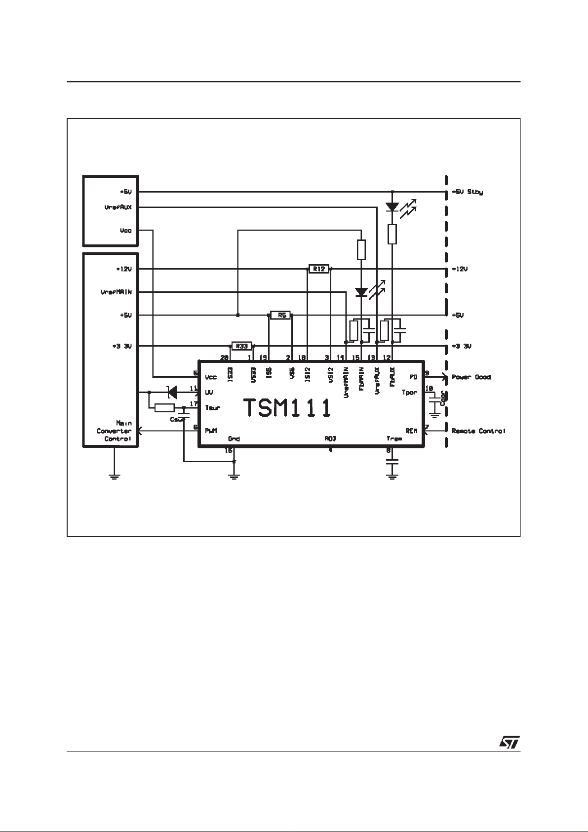
APPL ICATION DIAGRAM
6/18

TIMING DIAGRAM : remote control
TSM111
7/18
TSM111
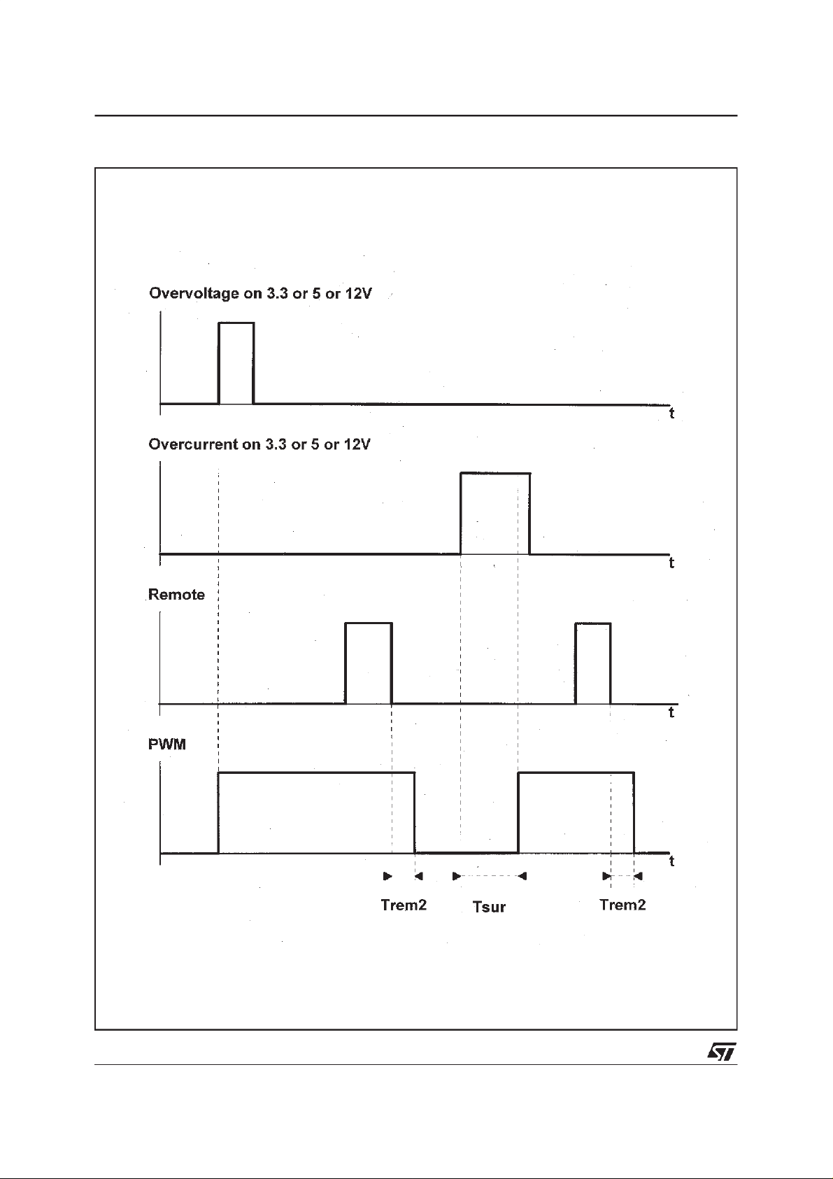
TIMING DIAGRAM : overvoltage o r overcurrent shut -down
8/18

TSM111
AN EXAMP LE O F 90W MI CR O A T X
POWER SUPPLY USING L5991A, VIPER2 0 AND TSM1 1 1
Protectionagainstaccidentalshort circuitsand fault
conditions is mandatory in PC power supplies.
These protection circuits can be realized by using
many discrete components which occupy a lot of
PCBspace,designtimeinfinetuningthecircuit and
also addto assemblingcosts.
ST’ssinglechipTSM111ICprovidescompleteprotectioncircuits designeasier, with fewernumber of
components.TSM111 is an idealsupervisorIC for
PC powersupplies.
The salient featuresand benefits of this device are
listedbelow :
a)Overvoltageprotectionfor3.3V,5Vand12Vwithout externalcomponent.
b) Over currentprotectionfor 3.3V,5V and 12V.
c) GeneratesPower Good signal.
d) Programmabletimingfor Power Good signal.
e) Wide range supply operating voltageup to 36V
(44VAMR).
f) Stableinternalvoltage reference.
g) Two 1.6% voltage referencefor Mainand Auxil-
iary regulation.
h) Few externalcomponents.
i) Circuitoccupieslittlespace on PCB.
j) Easyimplementation of thecircuit.
FEATURE DESCRIPTI ONS
a)Overvoltageprotectioncanbeimplementedwithout anyadditionalcomponents.Overvoltagesense
levelsfor3.3V,5V,12Vare4V,6.1V,14.2Vrespectively. With very little tolerances,betterprotectionis
achieved.
b) Overcurrent protectioncan beimplementedwith
very small value sense resistors. As the current
sense thresholdlevels are set very low,regulation
is not affected.The current sense threshold levels
for 3.3V, 5V, 12V are 50mV, 50mV and 65mV respectively.
c) The power goodsignal(pin9) isassertedto indicate the 5V and 3.3V is above the under voltage
thresholdlevel. PG pin goes high when the above
conditionis reached.Pull up resistorR27 (3.1K) is
connectedto 5V STDBY supplyfrom this pin.
d) The timing of thepowergood signalcan be controlledby adjustingthe valueofthechargingcapacitor on pin 10. With 2.2µF/16Vcapacitoron pin 10,
400msecturnon delayis achieved.
e) Thepower supplycanbe operatedfrom 14.5Vto
36V.TheV
mustalwaysbehigherthanthesupply
CC
voltageon the 12Vinput pin by 2V.i.e. if 14Vis appearing12V inputpin the Vcc must be> 16V.
A COMPLETE P C SMPS SECO NDARY SUPE RVI SOR
9/18

TSM111
f) Two internal high precision TL431 shunt regulatorsarebuilt-in.Itprovidesstablereferencevoltages
with a voltageprecisionof 1.6%.
SUPERVISORY CIRCUIT O PERATION
The system power ON/OFF logic is generated by
the PC,whichis ”Low” insystem”On” conditionand
”High” when the systemis ”Off”. This is connected
to remotepin 7.
TheIC’sinternallogiccircuitgeneratesacontrolsignal on pin 6. In normal operation,whenthere is no
over voltageor over currentat the threeinputs, the
voltageon pin 6 follows the Remote pin 7 voltage,
i.e. if the remotepin7 is lowthe pin 6is alsolow or
viceversa.
When fault is detected on the inputs, control pin 6
goes ”High”. This controlpin 6 output canbe used
to turnoff theMains PowerSupplyduringfault con-
dition. An optocoupler is connected directly, with
cathodeconnectedto the IC pin6 andanode to
5V (from STDBYsupply).
In normal operation the voltage on pin 6 is (opto
cathode)is around3.7 V. On the primary side the
opto transistor collectoris pulled througha resistor
to Vref.
It is requiredto invertthe signal before connecting
to the feedbackcompensationpin 6 of L5991A for
reverse logic.i.e duringnormaloperationthe compensationpin is not affectedand duringfaultconditionthe pinis pulledLow. Slightdelay (R34,C32)is
introducedonthe primary sideto avoidfaultturnon
condition.
Note : Once t he f ault condition is removed, it is requi r ed t o
reset t h e Remote pin to make t he system functi on again.
10/18

BILL OF MATERIAL
The following are the bill of material for the 90W SMPS :
No Part Number Qt Manufacturers Remarks/Descirptions
ICs
1 L5991A 1 ST Advanced PWM Controller
2 VIPer20DIP 1 ST Aux controller PWM+Mos
3 TSM111 1 ST Triple Voltage and Current Supervisor
4 LM7912CV 1 ST -12V Post Regulator
5 TL431 1 ST Programmable Voltage Reference
MOSFETs
6 STP6NB80 1 ST TO220 6A, 800V Mos
7 STP3020L 1 ST TO220 22mohm 30V Mos
Rectifiers
8 BYV10-40 1 ST 1A, 40V or BYV10-60 or BYW100-200
9 BYW100-200 3 ST 1A, 100V or 200V, BYW100-100
10 STPS20L40CT 1 ST 2x10A, 40V or STPS2045CT or
11 STSPS10L40CT 1 ST 2x5A, 40V
12 KAL04 1 - 3Amp 400VAC Bridge Rectifier or higher
13 1N4148 1 -
Transformers / Inductors
12 HM00-98150 1 BI Tech.** Aux Transformer
13 HM00-98151 1 BI Tech. Main Transformer
14 HM00-98148 1 BI Tech. Coupled inductors
15 HM50-150K 1 BI Tech. 15uH inductors - output filter
16 HM11-51502 1 BI Tech. 2.2uH Inductors - output filter
17 HM28-32022 1 BI Tech. Common Mode choke - AC input filter
18 10uH 1 - 10uH inductors - output filter
Connectors
19 AC input conn 1 20 20-pin conn:
39-01-2200
21 Fann connector 1 22 Fuse 3.5A 1 23 NTC 1 Siemens 2.2 ohm
24 TLP621 Optocoupler 3 Toshiba 100% transfer ratio
25 AC switch 1 26 115V-230V selector 1 -
1 Molex 20pin output connector with terminals
STPS30L40CT
Molex 39-00-0038
TSM111
11/18

TSM111
.... continued BILL OF MATERIAL
No Part Number Qt No Part Number Qt
Capacitors Resistors
27 47UF/25V 1 52 20K 1
28 3.9NF 1 53 47K,3W 1
29 .47UF/16V 1 54 100K,1/2W 2
30 1NF 2 55 5.1K 1
31 100UF/25 1 56 3 MOHM 1
32 .22UF/250V A.C 2 57 1OR 2
33 1000UF/10V 2 58 10 MOHM 1
34 3300UF/10 1 59 4.7K 5
35 470UF/16V 2 60 68K 1
36 2.2NF 2 61 680R 1
37 2.2UF/16 1 62 39K 1
38 470UF/25V 1 63 3.1K 1
39 4.7NF 4 64 470K 1
40 47UF/16V 1 65 100R 1
41 100UF/25V 3 66 10K 4
42 100UF/25V 1 67 3.3K 1
43 47NF 3 68 5 MOHM 1
44 220UF/200V 2 69 1K 1
45 1000UF/25V 1 70 330R 1
46 2.2UF 1 71 10,1/4W 2
47 1.5NF 1 72 470R 1
48 10NF 1 73 0.68 2
49 .1UF 1 74 6.8K 2
50 3.3NF 1
51 56NF 1
** BI T echnol o ies Pte Lt e
Phone No: 65 249- 1115
F ax No: 65 445-1983
Attn: Kelvin Lim, Sales Dept
12/18

TSM111
17V
C18
5VSTDBY
470uF/16V
L3
10uH
C35
+
D7
470uF/16
BYW100-200
6
7
T2
AUX TRANS
D5
D6
OPT
OPT
-12V
1
3
R43
C20
4.7K
470nF
R
X
C17
+
D8
100uF/25
BYW100-200
98
R9
47
D4
1N4148
2
Vcc
8
IC1
VIPER20
GND
3
1osc
comp4
7
DRAIN(out)
6
5
123456789
11121314151617181920
F
2
C40
1000uF/25V
D15
BYW100-200
12V
R
1K
L6
INDUCTOR
+
L2
COUPLEDINDUCTOR
D16
BYW100-200
T1
MAINSTRANS
1
C29
470uF/25V
R
680,1/2W
OUT
GND
IN
D13
BYW100-200
C
100uF/25V
IC7
2
L7912
C19
100uF/25V
D12
BYW100-200
12
64 3
R45
4.7K
IC10
TL431
GNDANALOG
R44
330
IC2
1
TLP621
2
34
1235
+
R
47uF/25V
8.2K
R15
5.1K
C13
C14
3.9nF
R16
4.7K
.47uF/16V
C16
1nF
5V
L4
2.2uH
R17
10
5
R10
47K
C3
+
220uF/200V
R11
100K,1/2W
NTC
2.2ohm
R28
470K
F1
3.5A
S1
CN1
SWSPST
CON1
CON3
10
CN3
R421KR38
C25
+
470uF/16V
C24
+
3300uF/10
D11
STPS2045CT C21
C12
4.7nF
VAR
C2
.22uF/250V A.CLF01
C1
.22uF/250V A.C
A.CINPUT
100V~240VA.C
12
3.3K
C38
R26
39K
47nF
C23
3.3V
1000uF/10V
Q3
C22
+
STP3020
1000uF/10V
D14
1N4148
D12
STP1060CT
2.2nF
R18
10
D3
21
OPT
D2
BYT11-800
C4
+
220uF/200V
R12
100K,1/2W
S2
SWSPST
D1
BRIDGE
R
OPT
PWOK
PSON/OFF
R29
R47
10K
R19
10mohm
C26
2.2nF
121110789
R23
680
IC4
12
43
TLP621
C9
C10
R10
10
D5
1N4148
C31
4.7nF
R9
4.7K
R8
6.8K
4.7nF
+
47uF/25V
R4
10
R
OPT
R17A
3.5mohm
R39
5mohm
9
14
15
R27
3.1K
R22
33K
12
C37
47nF
13
15
14
3
18
2
19
1
20
C34
100uF/25V
R13
10K
Q1
STP6NB80
R5
10
8
10 13 12
Vc
Vcc
OUT
DIS
DC-LIM
DC
R2
6.8K
C6
.1uF
4.7K
C41
2.2uF
910
FbAUX
PG
VrefAUX
FbMAIN
VrefMAIN
VS12
IS12
VS5
IS5
VS33
7
Tpor
REM
Trem
ADJ
TSM111
SUPERVISOR
IC6
Gnd
C51
8
100nF
R
4
20K
16
IS33
UV
11
D14
OPT
R24
10K
R7A
.22
R7A1
R7
D
1K
20V
R6
470
C11
1nF
SGNDPGND
L5991
16
C5
1.5nF
C55
10uF/35V
11
Tsur
17
C28
2.2uF/16
IC5
12
TLP621
R34
10K
R3
100
C7
3.3nF
IC3
6
L5991A
COMP
VFBSSSTBYRCTVREF
57
C8
56nF
PWM
34
C30
C32
R20
220uF/16V
4.7K
Q2
NPN1
4.7nF
+
Vcc
56
ISEN
IC3
234
13/18
TSM111
EVAL UATI ON BOARD - TECHNICAL NOTICE
TSM111 is a HousekeepingIC which is best used
in PC Switch Mode Power Suppliesfor secondary
3.3V,5V, and 12V power linesprotection.
TSM111integratesallthe necessaryfunctionsfor a
secure and reliable overcurrent and overvoltage
protection, as well as a logic interface for proper
communication with the motherboardand adjustable timing circuitry for optimized sequencingmanagement. Moreover, TSM111 integrates two preciseshuntvoltagereferencesfor direct optocoupler
drive. TSM111, integratingthe equivalent of more
than 25 discrete components,savesa lotof design
time and fine tuning, as well as PCB area, and increasesthereliabilityof thewhole application.
How to use the TSM111 EvaluationBoard?
Thisevaluation boardallows to adapt the TSM111
housekeepingchiptoanalreadyexistingPCPower
Supplyby simply choosingproper valuesfor it’sexternalcomponents,and makingthe adequateconnectionsto theI/O of the evaluationboard.
The ElectricalSchematicof theTSM111evaluation
boardis shownon figure1. It includesthe TSM111
as well as the minimum component number requiredto maketheTSM111 fitin a PCSMPS application.
Components calculations
Theovervoltageprotectionis notto be adjusted.Internalvoltage thresholdsare given by Vvs1, Vvs2,
Vvs3for respectiveprotectionof the 3.3V, 5V, 12V
powerlines.
Theovercurrentprotectionis given bythe choiceof
the Sense resistors R1, R2, R3 (respectively for
eachpowerline3.3V,5V,12V).Internalprecisevoltage thresholdsdefinethe trippingvoltagedrops for
each linefollowingequations1, 2 & 3 :
Vcs1= R1 x I33 eq1
Vcs2= R2 x I5 eq2
Vcs3= R3 x I12 eq3
whereI33, I5, and I12 are the trippingcurrents.
The system will latch (Fault output will be active -
high)if the overcurrentlasts more than the authorizedsurge delay Tsurgiven by equations4 & 5 :
Icharge= Vcc/ R4 eq4
Tsur= (C1 x Vsur) / Icharge eq5
Note that eq4 is an approximation of a capacitive
charge where Vcc (16V min) is large versus the
thresholdvoltage Vsur(2.5V).
R4=33kΩ, C1=4.7µF =>Tsur=21ms
Thanks to the Tsur adjustment, the normal surge
currents which occur during power up (capacitive
14/18
J3
Optaux
J16
VrefAux
J15
VrefMain
J7
IN12V
J6
In5V
J5
In3.3V
J1
Vdet
J2
Fault
J13
Vcc
J14
Gnd
EVALUATION BOARD - ELECTRICA L SCHEMATIC
Roptaux
1
19
Is5
Vs33
U1 TSM111
Vout
GND
1
R9
R2
rs5V
5Vstby
3
R10
R7
R8
Vcc
5
C6
RoptMain
R3
rs12V
2
18
Vs5
Is12
Gnd
16
C5
C4
3
14
15
Vs1 2
Vref Main
Adj
4
I
1INV
13
12
PG
FbAu x
Fbmain
Vref Au x
Tpor
Rem
TRem
8
R5 R rem
C2
Crem
5Vstby
9
10
7
1
Optaux
2
VrefAux
1
2
J18
1
OptMain
OptMain
1
2
1
1
1
1
2
1
2
1
2
1
2
2
VrefMain
In12V Out12V
In5V
11
17
6
20
Is33
UV
Tsur
PWM
U2 78L05
2
+
R1
rs3.3V
Vin
In3.3V
D1
Vdet
5Vstby
UV
R4
Rsur
R6
Fault
VCC
C1 Csur
C7
R11
Cpor
C3
Out5V
Out3.3V
PG 1
D6
From c
D5
SW1
5Vstby
12
34
BP Rem
1
1
1
2
1
2
1
2
J8
Out12V
J9
Out5V
J10
Out3.3V
J11
PG
J12
Rem
J20

TSM111
loadscharging)areblankedfor atimedependingon
eachapplication.
Whenthe systemhas latched(eitherafter overcurrent or overvoltagecondition),thesystem needsto
beresetviatheRemoteinput.The C2capacitordeterminestwo differenttimingsto the Fault output:
C2=100nF=> Trem1(ON to OFF)=8ms
C2=100nF=> Trem2(OFF to ON)=24ms
R5 is a pull down resistor on the remote pin of
TSM111.Note that an integratedpull up resistorof
100kΩ is to be taken into account in thechoice of
R5, knowingthat thethresholdvoltage of the input
comparatoris 1.4V. Therefore,R5 shouldbe lower
than38.8kΩ.
R5 = 1kΩ is agood value.
The evaluation board integrates the possibility to
maketheRemotesignaleithermanual,orelectronic
thanksto theORingdiodesD5 andD6 (andthepull
down resistor R5), and the Push Button (SW1).
Thesediodes can of course be replacedby straps
according to the evaluation requirements(manual
or electronic).
The Tpor delay time allows the PG output (Power
Good) to rise to high level when the 5V power line
internalsupervision circuitry has stayedabove the
undervoltage 4.3V threshold for more than Tpor
timefollowing the approximatedequation6 :
C3 x Vth = Ic x Tpor eq6
whereVth is 2V and Ic is 20µA.
C3=2.2µF=> Tpor=300ms
Whenthe 5Vpower linepasses underthe4.3V un-
dervoltage threshold,the Power Good signal (PG)
fallsimmediately to low level.
ThePowerGoodoutputcanalsobetriggeredbythe
Vdet input of the board. This input should be connected to a power line representative of the AC
mainspowersituation.Asanexample,anadditional
windingonthe auxiliary powersupplyoffer an early
warningof power downfromthemainspowerpoint
of view. The UV threshold is internally fixed to
Vdet=1.26V. Therefore, it is necessary to add a
zenerdiodeD1.
D1=15Vzener=> Vdet=16.26V
Note that a 20kΩ serial pull down resistor is inte-
grated. Therefore, only a low power zener is
needed.
The Faultoutput needsa pullup resistorR6.
The Power Good output needs a pull up resistor
R11. Both signals are pulled up to the 5Vstandby
power supply which can be generated from the
evaluation board thanks to a 78L05 5V regulator.
ThisregulatorneedsaC6bypasscapacitor.TheC7
bypass capacitor smoothens the V
CC
pin of
TSM111.
TheAdj(Adjust)pinshouldbeconnectedto ground.
Adjust allows to tune a newovervoltageprotection
value (ex2.7V insteadof 3.3V).
Exampleof componentlists
Table 1 gives an example of componentlist
Name Type Value Comment
U1 IC TSM111 DIP20
U2 IC 78L05 TO92
R1 R 1/4W
R 1/2W
R1W
R2 R 1/4W
R 1/2W
R1W
R3 R 1/4W
R 1/2W
R1W
R4 R 1/4W 33kΩ
R5 R 1/4W 1kΩ
R6 R 1/4W 47kΩ
R7 R 1/4W depends on opto used
R8 R 1/4W 10k
R9 R 1/4W depends on opto used
R10 R 1/4W 10k
R11 R 1/4W 47kΩ
D1 Z 1/4W 15V
D5 D 1/4W 1N4148
D6 D 1/4W 1N4148
C1 C Electro 4.7µF
C2 C Plastic 100nF
C3 C Electro 2.2µF
C4 C Plastic 10NF comp. network to
C5 C Plastic 10NF comp. network to
C6 C Plastic 100nF
C7 C Electro 10µF
10mΩ
5mΩ
2.5mΩ
10mΩ
5mΩ
2.5mΩ
65mΩ
13mΩ
6.5mΩ
Ω
comp. network to
be fine tuned
Ω
comp. network to
be fine tuned
be fine tuned
be fine tuned
5A
10A
20A
5A
10A
20A
1A
5A
10A
Figures2a and 2b show thecopper and silkscreen
sidesof theEvaluationboardPCB.
Notethat it is not a 1/1scale.
15/18

TSM111
Figure 2a Figure 2b
16/18

PACKAG E MECHANI CAL DATA
20 PINS -PLAS TIC DIP
TSM111
Dimensions
a1 0.254 0.010
B 1.39 1.65 0.055 0.065
b 0.45 0.018
b1 0.25 0.010
D 25.4 1.000
E 8.5 0.335
e 2.54 0.100
e3 22.86 0.900
F 7.1 0.280
I 3.93 0.155
L 3.3 0.130
Z 1.34 0.053
Min. Typ. Max. Min. Typ. Max.
Millimeters Inches
17/18

TSM111
PACKAG E MECHANI CAL DATA
20 PINS -PLASTIC MICROPACKAGE (SO)
Dimensions
Min. Typ. Max. Min. Typ. Max.
Millimeters Inches
A 2.65 0.104
a1 0.1 0.3 0.004 0.012
a2 2.45 0.096
b 0.35 0.49 0.014 0.019
b1 0.23 0.32 0.009 0.013
C 0.5 0.020
c1 45
o
(typ.)
D 12.6 13.0 0.496 0.512
E 10 10.65 0.394 0.419
e 1.27 0.050
e3 11.43 0.450
F 7.4 7.6 0.291 0.299
L 0.5 1.27 0.020 0.050
M 0.75 0.030
S8
Information furnished is believed to be accurate and reliable. However, STMicroelectronics assumes no responsibility for the
consequences of use of such information nor for any infringement of patents or other rights of third parties which may result
from its use. No license is granted by implication or otherwise under any patent or patent rights of STMicroelectronics.
Specifications mentioned in this publication are subject to change without notice. This publication supersedes and replaces all
information previously supplied. STMicroelectronics products are not authorized for use as critical components in life support
devices or systems without express written approval of STMicroelectronics.
Australia - Brazil - Canada - China - France - Germany - Italy - Japan - Korea - Malaysia - Malta - Mexico - Morocco
The Netherlands - Singapore - Spain - Sweden - Switzerland - Taiwan - Thailand - United Kingdom - U.S.A.
The ST logo is a trademark of STMicroelectronics
1999 STMicroelectronics – Printed in Italy – All Rights Reserved
STMicroelectronics GROUP OF COMPANIES
http://www.st.com
o
(Max.)
18/18
 Loading...