

1/13
■ CURRENT MEASUREMENT ON OUTPUT
POSITIVE LI NE
■ CONSTANT VOLTAGE MODE CONTROL
■ CONSTANT CURRENT MODE CONTROL
■ PRECISION VOLTAGE AND CURRENT
CONTROL LOOPS
■ ADJUSTABLE SWITCHING FREQUENCY
■ ADJUSTABLE OVER VOLTAGE LOCKOUT
■ ADJUSTABLE UNDER VOLTAGE LOCKOUT
■ STANDBY MO D E (L OW QUIESCE NT
CURRENT)
■ SUSTAINS 60V
■ MINIMAL EXTERNAL COMPONENTS
COUNT
■ DRIVING ABILITY FOR EITHER P-MOSFET
OR PNP TRANSISTORS
DESCRIPTION
TSM108 is a P-channel MOSFET controller which
ensures constant voltage and constant current in
Switching Mode Power Supply (step down) like in
automotive battery charging applications.
TSM108 can easily be configured for very wide
voltage and current needs.
TSM108 is built in rugged BCD technology and
includes a PWM generator, Voltage and Current
control loops, a precision Voltage Reference, and
a P-Mosfet Gate Drive output. TSM108 can
sustain 60V on Vcc, and therefore meet the
standard Load Dump requirements in the
Autom o tive field.
TSM108 includes security functions which lock the
PMosfet in OFF state: OVLO (Over Voltage
Lockout) and UVLO (Under Voltage Lockout). The
P-Mosfet Gate is also protected from over voltage
drive thanks to a 12V clamping protection circuit.
TSM108 includes a standby feat ure which allows
very low quiescent current when activated, as well
as safe P-Mosfet Off state .
TSM108 is suitable for car environment
accessories, as well as numerous other DC/DC
step down regulation.
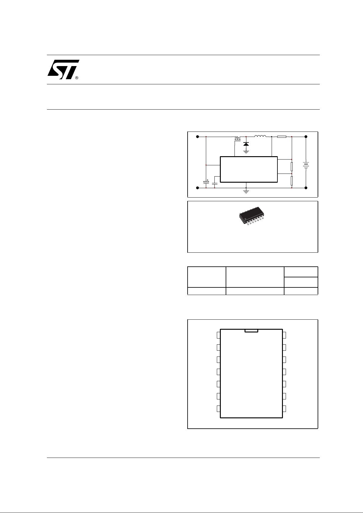
APPLICATION DIAGRAM
ORDER CODE
D = Small Outline Package (SO) - also available in Tape & Reel (DT)
PIN CONNECTIONS (top view)
Part Number Temperature Range
Package
D
TSM108I -40°, +125°C
•
MOSFET P
BATTERY
TSM108
DC INPUT
or PNP
D
SO14
(Plastic Micropacka ge)
VCC
G
OV
UV
ICTRL
OSC
GND
VCOM
P
VCTRL
ICOMP
VREF
VS
7
6
5
4
3
2
1
8
9
10
11
12
13
14 GD
!STBY
TSM108
AUTOMOTIVE SWITCH MODE
VOLTAGE AND CURRENT CONTROLLER
November 2001

TSM108
2/13
PIN DESCRIPTION
ABSOLUTE MAXIMUM RATINGS
OPERATING CONDITIONS
Name Pin Type Description
VCC 1 Power Supply Power Supply Line of the Device - Source of the P-MOSFET
GND 3 Power Ground 0V Reference for all Voltages
GD 14 Gate Drive Gate Drive Pin of the P-MOSFET - Middle Point of the MOSFET
Push Pull Output Stage
VREF 10 Output Voltage Reference Output
VS 13 HZ Input Voltage Sense Resistor Input
ICTRL 12 HZ Input Current Regulation Input
VCTRL 11 HZ Input Voltage Regulation Input
VCOMP 8 Output Compensation pin - Output of Voltage Control Op-Amp
ICOMP 9 Output Compensation pin - Output of Current Control Op-Amp
OSC 7 Input Oscillator Frequency Set Capacitor
!STBY 2 Input Standby Command (Command = 0V ===> Device Standby)
UV 4 I/O Programmable Under Voltage Lockout. The middle point of the
integrated resistor bridge is accessible. Preset value is 8V min.
OV 5 I/O Programmable Over Voltage Lockout. The middle point of the
integrated resistor bridge is accessible. Preset value is 33V max.
G 6 Test Pin Internally Connected to Ground
Symbol Parameter Value Unit
V
CC
Supply Voltage 60 V
T
j
Maximum Junction Temperature 150 °C
R
thja
Thermal Resistance Junction to Ambient (SO package) 130 °C/W
T
amb
Ambient Temperature -55 to +125 °C
V
max
Out Terminal Voltage (ICTRL, VS) 10 V
Symbol Parameter Value Unit
V
CC
Supply Voltage UVLO to OVLO V
V
ter1
Out Terminal Voltage (ICTRL, VS) 0 to 9 V
V
ter2
Out Terminal Voltage (UV, OV, OSC) 0 to 6 V

TSM108
3/13
ELECTRICAL CHARACTERISTICS
T
amb
= 25°C, VCC = 12V (unless otherwise specified)
Symbol Parameter Test Condition Min. Typ. Max. Unit
CURRENT CONSUMPTION
I
CC
Current Consumption 4 7 mA
STANDBY
I
stby
Current Consumption in Standby Mode 150
µ
A
V
sh
Input Standby Voltage High Impedance Internal Pull up resistor.
Stby pin should be left
open
2V
V
sl
Input Standby Voltage Low 0.8 V
OSCILLATOR
F
OSC
Frequency of the Oscillator C
OSC
= 220pF 70 100 130 kHz
VOLTAGE CONTROL 1)
2)
1. V
ref
paramete r i ndi cates glob al precision of the voltage control loop.
2. Control Gain : A
v
= 95dB ; Input R esistance : Rin = infinite ; Output Resistance : R
out
= 700MΩ ; Output Source/Sink Current :
I
so
, Isi = 150µA ; Recommended val ues for the com pensation network are : 22nF & 22kΩ in series bet ween outpu t and ground.
V
ref
Voltage Control Reference T
amb
= 25°C
-25°C < T
amb
< 85°C
2.450
2.520
2.590
V
CURRENT CONTROL 3) 4)
5)
3. V
sense
paramete r i ndi cated global precis i on of the current contro l lo op.
4. Control Gain : A
v
= 105dB ; Input Resistance : Rin =380kΩ ; Output Resistance : R
out
= 105MΩ ; Output Source/Sink Current :
I
so
, Isi = 150µA ; Recommended val ues for the com pensation network are : 22nF & 22kΩ in series bet ween outpu t and ground.
5. A current foldb ack function i s implemented thanks to a systema tic -6mV negat i ve offset on the current amplifier i nputs which
protects the battery fr om over charging current under low battery volt age conditi ons, or output short circui t conditions.
V
sense
Current Control Reference Voltage T
amb
= 25°C
-25°C < T
amb
< 85°C
196
191
206 216
221
mV
GATE DRIVE - P CHANNEL MOSFET DRIVE
I
sink
Sink Current - Switch ON T
amb
= 25°C
-25°C < T
amb
< 85°C
15
40 mA
I
source
Source Current - Switch OFF T
amb
= 25°C
-25°C < T
amb
< 85°C
30
80 mA
C
load
Input Capacitance of the PMOSFET
6)
6. The Gate Drive output stag e has been optim i zed for PMo sf ets with input capacitance equal to Cload. A bigger Mosfet (with input
capacitance higher than Cload) can be used with TSM108, but the gate drive performances will be reduced (in particular when
reaching the Dmax. PW M mode).
11.5nF
PWM
∆
max.
Maximum Duty Cycle of the PWM function 95 100 %
UVLO
UV
Under Voltage Lock Out
7)
7. The given limits comprise the hysteresis (UV
hyst
).
-25°C < T
amb
< 85°C 8 9 V
UV
hyst
UVLO Voltage Hysteresis - low to high 200 mV
R
uvu
Upper Resistor of UVLO bridge
8)
8. It is possible to m odify the UVLO and OVLO l i m i ts by adding a resi stor (to ground or to VCC) on the pins UV and OV.
The internal values of the resistor should be taken into account
T
amb
= 25°C 184 k
Ω
R
uvl
Lower Resistor of UVLO bridge (see note 8) T
amb
= 25°C 76.5 k
Ω
OVLO
OV Over Voltage Lock Out (see note 7) -25°C < T
amb
< 85°C 32 35 V
OV
hyst
OVLO Voltage Hysteresis - low to high 400 mV
R
ovu
Upper Resistor of OVLO bridge (see note 8) T
amb
= 25°C 275 k
Ω
R
ovl
Lower Resistor of OVLO bridge (see note 8) T
amb
= 25°C 23.2 k
Ω
TSM108
4/13
DETAILED INTERNAL SCHEMATIC
13
12
9
11
10
8
14
7
2
4
5
1
3
VS
ICTR
L
ICOMP
VCOMP
VREF
VCTR
L
Vsense
200mV
VREF
2,52V
GND
6
VCC
!STBY
UV
OV
OSC
GD
TSM108
10k
Ω
20µA
VCC
Ruvu
184k
Ω
Ruvl
76,5k
Ω
VREF
VCC
Rovu
275k
Ω
Rovl
23,2k
Ω
G
4,5V
15V
Oscillator block
Protection block
maximum duty cycle = 95%

TSM108
5/13
OSCILLATOR FREQUENCY VERSUS TIMING CAPACITOR
TSM108 AS A STAND ALONE DC/DC CONVERTER FOR CIGARETTE LIGHTER ACCESSORIES
0
50
100
150
200
250
300
350
10 100 1000
Oscilla tor freque ncy (kHz)
Cosc Timing Capacitor (pF)
Q1
MOSFET P
L1
Rsense
Csupply
load
L2
1
DC INPUT
1
Cf
Rf
R1
R2
1
DC OUTPUT
1
CompDComp
+
-
-
+
+-
Vcc
Gnd
!Stby
UV
OV
Vs
Vs
Ictrl
Icomp
Vcomp
Vref
Vctrl
G
Oscillator
Uv/Ov/Stby
Cosc
Osc

6/13
Description of a DC/DC step down battery
charging application
1. Voltage and Current Controller
TSM108 is designed to drive a P-Channel
MOSFET transistor in Switch Mode Step Down
Converter applications. Its two integrated
operational amplifiers ensure accurate Voltage
and Current Regulation.
The Voltage Control dedicated operational
amplifier acts as an error amplifier and compares
a part of the output voltage (external resistor
bridge) to an integrated highly precise voltage
reference (V
ref
).
The Current Control dedicated operational
amplifier acts as an error amplifier and compares
the drop voltage through the s ense resistor to an
integrated low value voltage reference (V
s
).
These two amplified errors are ORed through
diodes, and the resulting signal (“max of”) is a
reference for the PWM generator to set the
switching duty cycle of the P-Channel MOSFET
transistor.
The PWM generator comprises an oscillator (saw
tooth) and a comparator which gives a variable
duty cycle from 0 to 95%. This PWM signal is the
direct command o f the output Push Pull stage to
drive the Gate of the P-Channel MOSFET.
Thanks to this architecture, the TSM108 is ideal to
be used from a DC power supply to control the
charging Voltage and Current of a battery in
applications such as Automotive accessories for
Portable Phone charging and power supplies.
2. Voltage Control
The Voltage Control loop is to be set thank s to an
external resistor bridge connected between the
output positive line and the Ground reference. The
middle point is to be connected to the V
ctrl
pin of
TSM108, and, if R1 is the upper resistor, and R2,
the lower resistor of the bridge, the values of R1
and R2 should follow:
❑ eq1: Vref = Vout x R2 / (R1 + R2)
When under Constant Voltage Control mode, the
output voltage is fixed thanks to the R1/R2 resistor
bridge.
The total value of R1 + R2 resistor bridge will
determine the necessary bleeding current to keep
the Voltage Control loop effective, even under “no
load” conditions.
The voltage compensation loop is directly
accessible from the pins Vcomp and Vref
(negative input of the Voltage Control dedicated
operational amplifier). The c ompens ation net work
is highly dependant of the conditions of use of the
TSM108 (switching frequency, external
components (R, L, C), MOSFET, output
capacitor...).
3. Current Control
The Current control loop is to be set thanks to the
Sense resistor which is to be placed in series on
the output positive line. The output side of the
Sense resistor should be connected to the Ictrl pin
of TSM108, and the common point between
Rsense and the filtering self L should be
connected to the Vs pin of TSM108. If Ilim is the
value of the charging current limit The value of
Rsense should verify:
❑ eq2: V
s
= R
sense
x Il
im
When under Constant Current Control mode, the
output current is fixed thanks to the Rsense
resistor (under output short circuit conditions,
please refer to this corresponding section).
The wattage calibration (W) of the sense resistor
should be chosen according to:
❑ eq2a: W > R
sense
x Il
im
2
The current compensation loop is directly
accessible from the pins Icomp and Ictrl (negative
input of the Current Control ded icated operat iona l
amplifier.
The compensation network is highly dependant of
the conditions of use of the TSM108 (switching
frequency, external components (R, L, C),
MOSFET, output capacitor...).
4. PWM frequency
The internal oscillator of T SM108 is a saw tooth
waveform that can be frequency adjusted.
In automotive accessory battery charging
applications, it is recommended to set the
switching frequency at a typical 100kHz in order to
PRINCIPLE OF OPERATION AND APPLICATION HINTS
TSM108

TSM108
7/13
obtain the best compromise between electrical
noise, and size of the filtering self.
An external capa citor is t o be connected betwe en
ground and the Osc pin of TSM108 to set the
switching frequency.
The maximum duty cycle of the PWM function is
limited to 95% in order to ensure safe driving of
the MOSFET.
5. Gate Drive
The Gate Drive stage is directly commanded from
the PWM output signal. The Gate Drive stage is a
Push Pull Mosfet s tage which bears different On
resistances in order to ensure a slower turn ON
than turn OFF of the P-Channel MOSFET. The
values of the output Gate Drive currents are given
by Isink (switch ON) and Isource (switch OFF).
The Gate Drive stage bears an i nteg rated vo ltage
clamp which will prevent the P-Channel MOSFET
gate to be driven with voltages higher than 15V
(acting like a zener diode between Vcc and GD
(Gate Drive) pin.
6. Under Voltage Lock-Out, Over Voltage
Lock-Out
The UVLO and OVLO security functions aim at the
global application security.
When the Power supply decreases, there is the
inherent risk to drive the P-Channel MOSFET with
insufficient Gate voltage, and therefore to lead the
MOSFET to linear operation, and to its
destruction.
The UVLO is an input power supply voltage
detection which imposes a complete switch OFF
of the P-Channel MOSFET as soon as the Power
Supply decreases below UV. To avoid un wanted
oscillation of the MOSFET, a fixed hysteresis
margin is integrated (UVhyst).
UVLO is internally programmed to ensure 8V min
and 9V max, but the middle point of the integrated
resistor bridge is accessible and the value of t he
UVLO is therefore adjustable by adding an
external resistor to modify the bridge ratio. The
resistor typical values of the bridge are given
(Ruvh, Ruvl).
When the Power supply increases, there is the
inherent risk to dissipate too much conduction
energy through the P-Channel MOSFET, and
therefore to lead to its destruction.
The OVLO is an input power supply voltage
detection which imposes a complete switch OFF
of the P-Channel MOSFET as soon as the Power
Supply increases above O V. To avoid unwanted
oscillation of the MOSFET, a fixed hysteresis
margin is integrated (OV
hyst
).
OVLO is internally programmed to ensure 32V
min. and 33V max., but the middle point of the
integrated resistor bridge is accessible and the
value of the OVLO is therefore adjustable by
adding an external resistor to modify the bridge
ratio.
The resistor typical values of the bridge are given
(R
ovh
, R
ovl
).
Examples:
Let’s suppose that the internally set value of the
UVLO and / or OVLO level should be modified in a
specific application, or under specific
requirements.
6.1. UVLO decrease:
If the UVLO level needs to be lowered (UV 1), an
additional resistor (Ruvh1) must be connected
between UV and Vcc following the equation:
❑ UV = Vref (Ruvh/Ruvl +1)
❑ UV1 = Vref ((Ruvh//Ruvh1)/Ruvl +1) (i)
where Ruvh//Ruvh1 means that Ruvh1 is in
parallel to Ruvh
Solving i. we obtain:
❑ Ruvh1 = Ruvl x Ruvh (UV1 - Vref) / (Vref x
Ruvh - Ruvl (UV1 - Vref))
As an example, if UV1 needs to be set to 6V,
Ruvh1 = 256kΩ
6.2. UVLO increase:
If the UVLO level needs to be increased (UV2), an
additional resistor (Ruvl2) must be connected
between UV and Gnd following the equation.
❑ UV = Vref (Ruvh/Ruvl +1)
❑ UV1 = Vref (Ruvh/(Ruvl//Ruvl2) +1) (ii)
where Ruvl//Ruvl2 means that R uvl2 is in parallel
to Ruvl
Solving ii. we obtain:
❑ Ruvl2 = Vref x Ruvh Ruvl / (UV2 x Ruvl -
Vref x (Ruvh + Ruvl))
As an example, if UV2 needs to be set to 12V,
Ruvl2 = 132kΩ
6.3. OVLO decrease:
If the OVLO level needs to be lowered (OV1), an
additional resistor (Rovh1) must be connected
between OV and Vcc following the equation:
❑ OV = Vref (Rovh/Rovl +1)
❑ OV1 = Vref ((Rovh//Rovh1)/Rovl +1) (iii)
where Rovh//Rovh1 means that Rovh1 is in
parallel to Rovh
Solving iii. we obtain:
❑ Rovh1 = Rovl x Rovh (OV1 - Vref) / (Vref x
Rovh - Rovl (OV1 - Vref))
As an example, if OV1 needs to be set to 25V,
Rovh1 = 867kΩ

TSM108
8/13
6.4. OVLO increase:
If the OVLO level needs to be increased (OV2), an
additional resistor (Rovl2) must be connected
between OV and Gnd following the equation.
❑ OV = Vref (Rovh/Rovl +1)
❑ OV2 = Vref (Rovh/(Rovl//Rovl2) +1) (iv)
where Rovl//Rovl2 means that R ovl2 is in parallel
to Rovl
Solving iv. we obtain:
❑ Rovl2 = Vref x Rovh Rovl / (OV2 x Rovl -
Vref x (Rovh + Rovl))
As an example, if OV2 needs to be set to 40V,
Rovl2 = 87kΩ
7. Standb y Mode
In order to reduce to a minimum the current
consumption of the TSM108 when in inactive
phase, the Standby mode (!STBY pin of TSM108)
imposes a complete OFF state of the P-Channel
MOSFET, as well as a complete shut off of the
main functions of the TSM108 (operational
amplifier, PWM generator and oscillator, UVLO
and OVLO) and therefore reduces the
consumption of the TSM108 to the Istby value.
This !STBY command is TTL compatible, which
means that it can be directly commanded from
whatever logic signal.
8.Power Transistor: P-MOSFET or PNP
Transistor?
The TSM108 can drive, with minor external
components change, either a P-channel
MOSFET, or a PNP transistor. The choice of the
transistor is completely to the user’s responsibility,
nevertheless, here follows a few elements which
will help to decide which is the most adapted
transistor to drive depending on the application
characteristics in terms of power and
performances.
The following figures shows two different
schematics where both driving abilities of TSM108
are shown. The third schematic shows how to
improve the switch off commutation when using a
bipolar PNP transistor.
P- MOSFET? PNP Transistor?
The most immediate way to choose from a
P-channel MOSFET or a PNP transistor is to
consider the ratio between the output power of the
application and the expected components price:
the lower the power, the more suitable the PNP
transistor is; the higher the power, the more
suitable the P-channel MOSFET is. As an
example, for a DC/DC adaptor built for 12V/6V,
the recommended limit to choos e from one to the
other is situated around 200mA.
Below 200mA, the price/ performance ratio of the
PNP transistor is very attractive, whereas above
200mA, the P-channel Mosfet takes the
advantage.
9. Calculation of the Passive Elements
Let’s consider the following characteristics for a
Cigarette Lighter Cellular Phone Battery Charger:
Vin = 12V - input voltage of the converter
Vout = 6V - output voltage of the converter
F = 100kHz - switching frequency of the converter
adjustable with an external capacitor
Iout = 625mA - output current limitation
9.1. Inductor
The minimum inductor value to choose should
apply to
Lmin = (1 - D) R / 2F
where R = Vout / Iout = 9.6Ω
and where D = Vout / Vin = 0.5
Therefore, Lmin = 24µH.
L1
GD
D1
TSM108
Q1
MOSFET P
Q1 L1
GD
D1
TSM108
Q1 L1
GD
D1
TSM108

TSM108
9/13
This component value is valid if the above
described characteristics are fixed... but in the
automotive field, the input voltage of the converter
is dependant of the car bat tery conditions. Also,
the frequency may vary depending on the
temperature, due to the fact that the frequency is
fixed by an external capacitor. Therefore, we must
calculate the inductor v al ue considering the worst
case condition in order to av oid the saturation of
the inductor, which is when the batt ery voltage is
at it’s highest, and the switching frequency at it’s
lowest. Thanks to the OVLO function integrated in
TSM108, the operation of the DC/DC converter
will be stopped as soo n as the voltage exceeds
the OVLO level. Let’s suppose the O VLO pin has
been left open, therefore, the maximum input
voltag e of the D C / D C converter will b e V in max. =
32V. Frequency min stands in the range of 75kHz
In this case, D = 6 / 32 = 0.1875, therefore Lmin =
52µH.
If we allow a 25% security margin
Lmin = 68µH
9.2. Capacitor
The capacitor choice will depend mainly on the
accepted voltage ripple on the output
Ripple = DVout / Vout = (1-D) / 8LCF²
Therefore, C = (1-D) / 8LRippleF². If C = 22µF,
then Ripple = 0.4% which should be far
acceptable.
Here again, the worst co nditions for t he ripple are
set when the input voltage is a t the highest (32V )
and the frequency at it's lowest (75kHz).
with C = 22µF, Ripple = 1.2%
9.3. Ratings for the Inductor, Capacitor,
Transistor and Diode
The inductor wire must be rated at the rms c urrent,
and the core should not saturate for peak inductor
current. The capacitor must be selected to limit the
output ripple to the design specifications, to
withstand peak output voltage, and to carry the
required rms current.
The transistor and the diode should be rated for
the maximum input voltage (up to 60V in
automotive applications). The diode recovery time
must be in accordance with the time period a nd
the maximum authorized switching time of the
power transistor.
A compromise between the switching and
conducting performances of the transistor must be
found, because choosing a very low ohmic Mosfet
aiming at the benefit of low conduction losses may
bring much higher switching losses than the
expected benefit.
Losses in the switch are:
Pswitch = Prise + Pfall + Pon
where Prise + Pfall represent the switching losses
and where Pon represents the conduction losses.
Prise + Pfall = Iout x Vin x (Trise + Tfall) x F / 2
Pon = Ron x Iout² x d
where Trise is the switching on time, and Tfall is
the switching off time, and where d is the duty
cycle of the switching profile, which can be
approximated to 1 under full load conditions.
With the two last equations, we can see easily that
what we may gain by choosing a performing low
Rdson P-channel M OSF ET (for example) may be
jeopardized by the long on and off switching times
required when using a large input gate
capacitance.
10. Electromagnetic Compatibility
The small schematic hereafter shows how to
reduce the EMC noise when used in an EMC
sensitive environment:
EMC Improvement
The RC components should realize a time
constant corresponding to one tenth of the
switching time constant of the TS M10 8 (i.e. in our
example, the oscillator frequency is set to 10µs
corresponding to 100kHz, therefore, the RC
couple should realise a time constant close to
1µs).
Choosing the componen ts must privilege a rather
small resistivity (between 10 to 100W). A guess
couple of values for RC in our example would be:
R= 22W, C= 47nF
11. Efficiency Calculations (rough estimation)
The following gives a rough estimation of the
efficiency of a car phone charger, knowing that the
exact calculations depend on a lot of paramete rs,
as well as on a wide choice of external
components.
Let’s consider the following characteristics of a
classical car phone charger application:
L1
GD
D1
TSM108
Q1
MOSFET P

TSM108
10/13
❑ Vin = Vcc = 12V, Iout = 625mA, Vout = 6V
❑ Mosfet: Pchannel Mosfet: Rdson = 100mΩ,
Ciss = 1nF.
❑ Driver: TSM108
❑ PWM frequency: 100kHz
❑ Free wheel diode: Vf = 0.7V
❑ Shunt: Rsense = 330mΩ
The efficiency (η) of a regulator is defined as t he
ratio of the charging power (Pout) to the total
power from the supply (Pin).
❑ Eq3: η = Pout/Pin
The output power is:
Pout=Iout x Vout where Iout is the charging
current (Vsense/Rsense = 625mA at full load) and
Vout is the regulated voltage (Vref(1+R1/R2) =
6V).
Pout = 3.75W
The input power can be found by adding the
output power (Pout) to the total power loss in the
circuit (Plosses) i.e.
❑ Pin = Pout + Plosses
The power is lost partly on the chip and partly on
the external components which are mainly the
diode, the switch and the shunt. Plosses = Pchip +
Pswitch + Pdiode + Pshunt.
In Plosses, we neglect the losses in the inductor
(because the current through the inductor is
smoothened making the serial resistor of the
inductor very low), and the losses in the Gate
(charge and discharge).
a. The power lost in the chip is Pchip = Vcc x Icc.
(Vcc = 12V, Icc = 6mA) Pchip = 72mΩ
b. The power lost in the switch depends on the ON
resistance of the switch and the c urrent passing
through it. Also there is power loss in the switch
during switching time (commutation losses) and
that depends on the switching freq uency and the
rise and fall time of the switching signal.
Rise time (Pchannel goes off) depends on the
output source current of the TSM108 and the input
gate capacitance of the Mosfet.
Trise = Ciss x Vgate / Isource
Fall time (Pchannel goes on) depends on the
output sink current of the TSM 108 and the input
gate capacitance of the Mosfet .
Tfall = Ciss x Vgate / Isink
Trise = 150ns and Tfall = 300ns (Vgate is approx
12V).
❑ Pswitch = Prise + Pfall + Pon
where:
Prise = Iout x (Vcc+Vf) x Trise x PWMfreq / 2
Prise = 625mA x 12.7 x 150ns x 100kHz / 2.
Prise = 59.5mW
where:
Pfall = Iout x (Vcc+Vf) x Tfall x PWMfreq / 2
Pfall = 625mA x 12.7 x 300ns x 100kHz / 2.
Pfall = 119.1mW
where:
Pon = Rdson x Iout² x D (where D is the duty cycle
- at full charge, D can be approximated to 1)
Pon = 100mΩ x 625mA². Pon = 39.1mW
❑ Pswitch = 217.7mW
c. The power lost in the fly back diode is Pdiode =
Vf x Iout(1-D) where D = Vout/Vcc = 6/12. D = 0.5
❑ Pdiode=219mW
d. the power lost in the sense resistor (shunt
resistor) is Pshunt = Rsense x Iout²
❑ Pshunt = 129mW
Therefore,
Plosses = Pchip+Pswit ch+P diode +P shunt
= 72mW + 217.7mW + 219mW + 129m W
❑ Plosses = 638mW
The yield (efficiency) is
❑ Pout / Pin = 3.75 / (3.75 + 0.638) = 85.5%
η
= 85.5%
The following table gives a tentative efficiency
improvement view following the choice of some
external components. Be aware that some of the
following choices have non negl igible cost effects
on the total application.
Improved efficiency - by changing the external comp on ents value one by on e
Rsense 330m
Ω
220m
Ω
---Iout 625mA 936mA - - - Vout (R1/R2) 6V - 7.5V - - Rdson 100m
Ω
- - 140m
Ω
-Ciss 0nF - - 0.85nF - PWM Freq 100kHz - - - 50kHz Free Wheel 0.7V - - - - 0.3V
Yield 85.5% 85.6% 88.9% 85.7% 87.3% 88.1%
Cost influence - ==<>>>

TSM108
11/13
12. Measured Performances
The few following curves show the measured
performances of TSM108 used in DC/DC step
down converter, either with a Pchannel MOSFET
or with a PNP bipolar transistor.
12.1. Voltage and Current Control, Efficiency Performances using a Pchann el MOSFET :
0 0.1 0.2 0.3 0.4 0.5 0.6 0.7
Iout (A)
0
1
2
3
4
5
6
7
Vout (V)
0%
10%
20%
30%
40%
50%
60%
70%
duty cycle on (%)
CV & CC Regulation - Switching duty cycle vs Iout
Vin = 12V, Vout = 6V, Iout = 600mA
0 0.1 0.2 0.3 0.4 0.5 0.6 0.7
Iout (A)
0%
10%
20%
30%
40%
50%
60%
70%
80%
90%
100%
Efficiency (%)
0%
10%
20%
30%
40%
50%
60%
70%
80%
90%
100%
duty cycle on (%)
Converter efficiency & Switching duty cycle vs Iout
Vin = 12V, Vout = 6V, Iout = 600mA
5 1015202530 35
Vin (V)
5.992
5.993
5.994
5.995
5.996
5.997
5.998
5.999
6
6.001
Vout (V)
77%
78%
79%
80%
81%
82%
83%
84%
85%
86%
Efficiency (%)
Vout & Ef ficiency versus Vin
Vout = 6V, Iout = 600mA

TSM108
12/13
12.2. Voltage and Current Control, Efficiency Performances using a PNP bipolar transistor
0 0.05 0.1 0.15 0.2 0.25
Iout (A)
0
1
2
3
4
5
6
7
Vout (V)
0%
10%
20%
30%
40%
50%
60%
70%
duty cycle on (%)
PNP transistor Rbase = 220 L=150µH
Vout & duty cycle ver sus Iout
Vin=12V, Vout=6V , Iout=200m A
0 0.05 0.1 0.15 0.2 0.25
Iout (A)
0%
10%
20%
30%
40%
50%
60%
70%
80%
Efficiency (%)
0%
10%
20%
30%
40%
50%
60%
70%
80%
duty cycle on (%)
PNP transistor Rbase = 220 L=150µH
Efficiency & duty cycle versus Iout
Vin=12V, Vout=6V, Iout=200mA
5 101520253035
Vin (V)
6.025
6.03
6.035
6.04
6.045
6.05
Vout (V)
60%
65%
70%
75%
80%
85%
Efficicency (%)
PNP transistor Rbase =220 L=150µH
Vout & Efficiency versus Vin
Vout = 6V, Iout = 200mA

TSM108
Information furnished is believed to be accurate and reliable. However, STMicroelectronics assumes no responsibility for the consequences
of use of su ch i n for mat i on n or f or a ny in fr ing em ent o f pa te nts or ot her r igh ts of th ir d pa r tie s w hic h may res ul t f rom i ts us e. No license is granted
by impl i cation or ot herwise under any patent or patent r i ghts of STM i croelectronics. Specificat i ons mentio ned in this publicat ion are subject
to change without notic e. T hi s publicati on supersedes and replaces all informat i on previou sly supplied . S T M i croelectronics produc ts are not
authori zed for use as critical com ponents in l i fe support devices or systems without express written ap proval of STM i croelectr o nics.
© The ST logo is a registered trademark of STMicroelectronics
© 2001 STMicroelectronics - Printed in Italy - All Rights Reserved
STMicr oelectronics GROUP OF COMPANIES
Australi a - Brazil - Chi na - Finlan d - F rance - Germ any - Hong Kong - India - It al y - Japan - Ma l aysia - Malta - Morocco
Singapo re - Spain - Sweden - Switzerland - United Ki ngdom
© http://www.st.com
13/13
PACKAGE MECHANICAL DATA
14 PINS - PLASTIC MICROPACKAGE (SO)
Dim.
Millimeters Inches
Min. Typ. Max. Min. Typ. Max.
A 1.75 0.069
a1 0.1 0.2 0 .004 0.008
a2 1.6 0.063
b 0.35 0.46 0.014 0.018
b1 0.19 0.25 0.007 0.010
C 0.5 0.020
c1 45° (typ.)
D (1) 8.55 8.75 0.336 0.344
E 5.8 6.2 0.228 0.244
e 1.27 0.050
e3 7.62 0.300
F (1) 3.8 4.0 0.150 0.157
G 4.6 5.3 0.181 0.208
L 0.5 1.27 0.020 0.050
M 0.68 0.027
S 8° (max.)
Note : (1) D and F do not include mold flash or protrusions - Mold flash or protrusions shall not exceed 0.15mm (.066 inc) ONLY FOR DATA BOOK.
 Loading...