


VOLTAGE AND CURRENTCONTROLLER
.
1.24V SERIES VOLTAGE REFERENCE WITH
10mA OUTPUT CURRENT AND 1% PRECISION (TSM101A)
.
TWO OPERATIONAL AMPLIFIERS WITH
ORED OUTPUT AND 1MHZ GAIN BANDWIDTH PRODUCT
.
BUILT-IN CURRENT GENERATOR WITH ENABLE/DISABLEFUNCTION
.
4.5 TO 32V SUPPLYVOLTAGERANGE
.
SO8, DIP8 AND TSSOP8PACKAGES
TSM101/A
N
DIP8
(Plastic Package)
(Thin ShrinkSmall Outline Package)
(Plastic Micropackage)
P
TSSOP8
D
SO8
DESCRIPTION
The TSM101/TSM101Aintegratedcircuit incorporates a highstabilityseries bandgapvoltagereference, two ORed operational amplifiers and a
current source.
This IC compares the DC voltage and the current
level at the output of a switching power supply to
an internal reference. It provides a feedback
throughan optocouplerto the PWMcontroller IC in
the primaryside.
The controlled current generator can be used to
modify the level of current limitation by offsetting
the information coming from the current sensing
resistor.
APPLICATIONS
This circuitisdesignedtobe used in battery chargers with a constant voltage and a limited output
current.
Itcanbeusedineverytypesofapplicationrequiring
a precision voltage regulation and current limitation.
Other applications include voltage supervisors,
over voltageprotection...
ORDERCODES
Part Number
TSM101C/AC -20, +80
TSM101I/AI -40,+105
PIN CONNECTIONS
Temperature
Range
1
2
3
4
Package
o
Vref
NDP
C •••
o
C •••
8
7
6
5
June 1999
1/15
TSM101/A
ABSOLUTEMAXIMUM RATINGS
Symbol Parameter Value Unit
V
CC
I
out
P
V
I
in
T
stg
T
T
thja
Notes : 1. All voltages values, except differential voltage are with respectto network ground terminal
OPERATING CONDITIONS
Symbol Parameter
V
CC
T
oper
DC Supply Voltage - (note 1) 36 V
Output Current - (note 2) 20 mA
Power Dissipation 200 mW
d
Input Voltage - (note 3) -0.3, VCC-1.5 V
in
Input Current ±1mA
Storage Temperature -40 to +125
Maximum Junction Temperature 150
j
Thermal Resistante Junction to Ambiant 130 to 200
2. The voltagereference isnot protected against permanent short circuit
TSM101C/AC/I/AI
Value
Supply Voltage 4.5 to 32 V
Operating FreeAir TemperatureRange T
min.
to T
max.
o
o
o
C/W
Unit
o
C
C
C
ELECTRICAL CHARACTERISTICS
=25oC, VCC=15V (unless otherwisespecified)
T
amb
OPERATIONALAMPLIFIER : TSM101C/I/AC/AI
Symbol Parameter Test Conditions Min. Typ. Max. Unit
Total Supply Current VCC= 15V 2 mA
I
CC
Input Voltage Range 0 VCC-1.5V V
V
i
Input Offset Voltage 25oC
V
io
I
Input Bias Current
ib
Output Sink Current, Vol= 2.5V 25oC
I
sink
A
Large Signal Voltage Gain RL=2kΩ
vo
= 1.2V on pin 7 and Vin= 0V on pin 5 25oC
@V
in
SVR Supply VoltageRejection Ratio T
CMR Common Mode Rejection Ratio T
GBP Gain Bandwidth Product V
Output Leakage Current 25oC
I
oh
CC
V
in
T
min.<Tamb.<Tmax.
T
min.<Tamb.<Tmax.
T
min.<Tamb.<Tmax.
T
min.<Tamb.<Tmax.
min.<Tamb.<Tmax.
min.<Tamb.<Tmax.
= 15V, F = 100kHz
= 10mV, RL = 2kΩ
= 100pF
C
L
T
min.<Tamb.<Tmax.
-5
-7
-700
-1000
15
7
-300 0
0
15 mA
8
15
65 90 dB
80 dB
1 MHz
2
7
V/mV
mV
nA
µA
2/15
ELECTRICAL CHARACTERISTICS
=25oC, VCC=15V (unlessotherwisespecified)
T
amb
VOLTAGEREFERENCE : TSM101
TSM101/A
Symbol Parameter Test Conditions
Reference Voltage I
V
ref
Temperature Stability T
K
vt
R
R
Load Regulation 1 < I
eglo
Line Regulation 5 < Vin< 32V 3.5 10 3.5 10 mV
egli
= 1mA, T
out
min.<Tamb.<Tmax.
out
=25oC 1.21 1.24 1.27 1.21 1.24 1.27 V
amb.
< 10mA 5 15 5 15 mV
VOLTAGE REFERENCE : TSM101A
Symbol
V
ref
K
vt
R
eglo
R
egli
Parameter
Reference Voltage I
Temperature Stability T
Load Regulation 1 < I
Test Conditions
= 1mA, T
out
min.<Tamb.<Tmax.
amb.
< 10mA 5 15 5 15 mV
out
=25oC 1.227 1.24 1.252 1.227 1.24 1.252 V
Line Regulation 5 < Vin< 32V 3.5 10 3.5 10 mV
CURRENT GENERATOR : TSM101,TSM101A
Symbol Parameter Test Conditions
Current Source 1.4 1.4 mA
I
o
Temperature Stability T
K
cgt
Line Regulation 4.5 < VCC< 32V 0.003 0.03 0.003 0.03 mA
C
glir
V
V
I
I
csleak
Voltage at the enable
csen
pin to have
= 1.4mA
I
O
Voltage at the enable
csdis
pin to have
= 0mA
I
O
Input Current on the
csen
pin
C
sen
Leakage Current Vcs=2V
min.<Tamb.<Tmax.
T
min.<Tamb.<Tmax.
T
min.<Tamb.<Tmax.
T
min.<Tamb.<Tmax.
T
min.<Tamb.<Tmax.
TSM101C TSM101I
Min. Typ. Max. Min. Typ. Max.
Unit
30 100 35 120 ppm/oC
TSM101AC TSM101AI
Min. Typ. Max. Min. Typ. Max.
Unit
30 100 35 120 ppm/oC
TSM101C/AC TSM101I/AI
Min. Typ. Max. Min. Typ. Max.
Unit
500 600 ppm/oC
0.6 0.6 V
22V
30 30 µA
µA
0.5 2 0.5 2
3/15
TSM101/A
8
Vref
Gnd
1
4
7
Vref
Vrin
Cse n
Crref
Crin
2
3
5
DESCRIPTION
Name Pin Type Function
V
ref
V
rin
C
rin
C
rref
C
sen
OUTPUT 6 OUTPUT Output pin common to the voltage regulation and current limitation
V
CC
GND 4 INPUT Ground
1 OUTPUT Voltage Reference Output 1.24V, 10mA max. Do notshort circuit
7 INPUT Voltage Regulation Loop Input
5 INPUT Current Limitation Loop Input, connected to the sense resistor
3 INPUT Current Limitation Reference Input
2 INPUT Current source enable input. This current source can be used to
offset the voltage measurement on the sense resistor and therefore to
modify the charge current. The current source is enabled when the
input voltage on pin 2 is lower than 0.8V.
loops. This output can drivethe primary side (LED) of an optocoupler.
8 INPUT Power Supply Input (4.5 to 32VDC)
+Vcc
6
OUTPUT
4/15

TSM101/A
APPLICATION NOTE
A BATTERY CHARGER USING THE TSM101
by S. LAFFONT and R. LIOU
This technical note showshow to use theTSM101
integrated circuit with a switching mode power
supply(SMPS) to realize a battery charger.
An exampleof realizationofa12VNickel-cadmium
battery chargeris given.
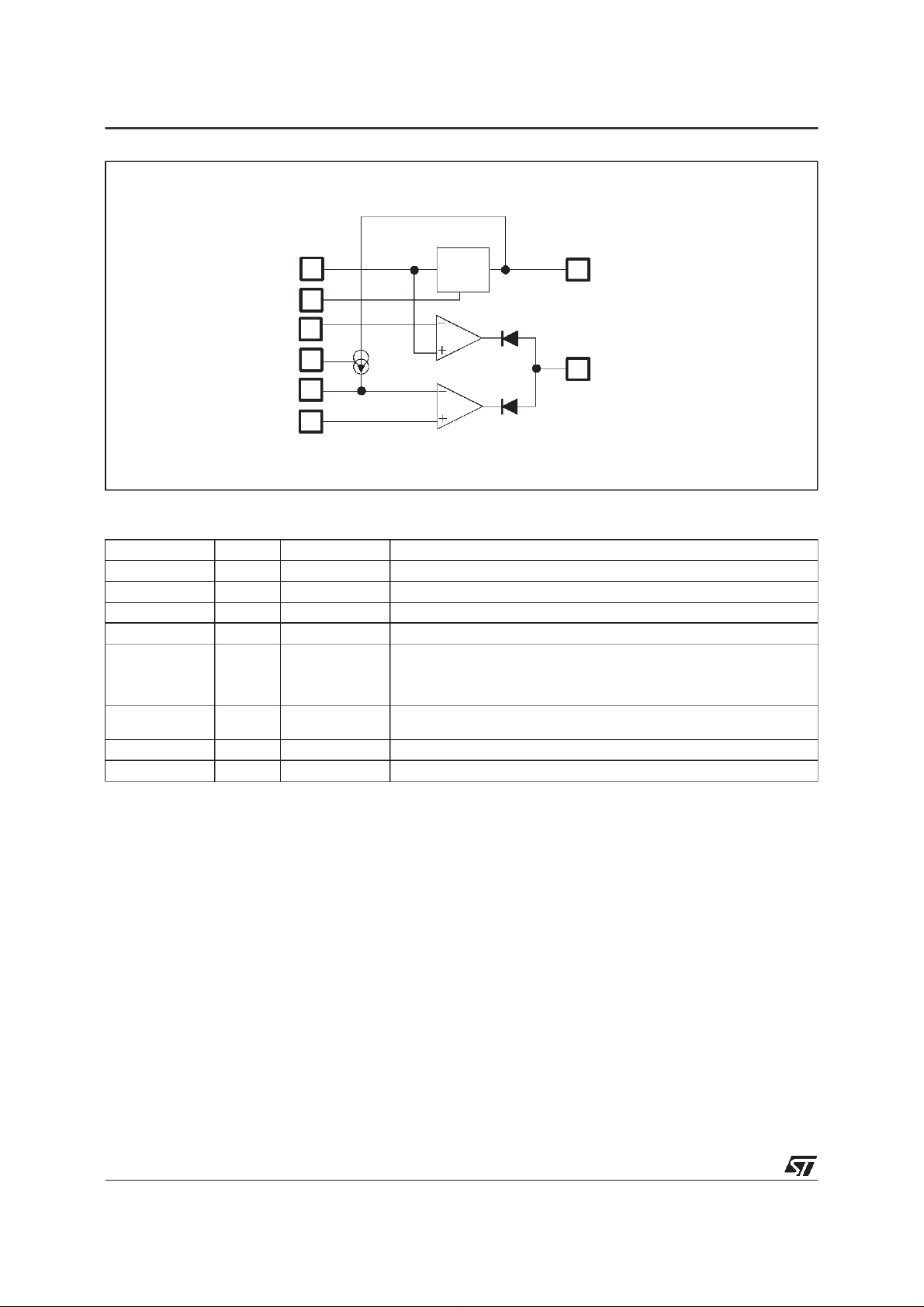
1 - TSM101PRESENTATION
The TSM101integratedcircuit incorporatesahigh
stability series band gap voltage reference, two
ORed operational amplifiers and a current source
(Figure 1)
Figure 1 : TSM101Schematic Diagram
1
Vref
2
3
4
This IC compares the DC voltage and the current
level at the output of a switching power supply to
an internal reference.It provides a feedback
throughan optocouplerto the PWMcontroller IC in
the primaryside.
The controlled current generator can be used to
modify the level of current limitation by offsetting
the information coming from the current sensing
resistor.
8
7
6
5
A great majority of low or medium end power
supplies is voltage regulated by using shunt programmablevoltage referenceslike the TL431
(Figure 2).
Thegalvanic insulation of the controlinformationis
doneby using an opto-couplerin linearmode with
a variable photo current depending on the difference between the actual output voltage and the
desiredone.
A current limitation is used to protect the power
supply against short circuits, but lacks precision.
This limitation is generally realized by sensing the
currentof the power transistor,in the primaryside
of the SMPS.
Therole of theTSM101isto makea fineregulation
of the output current of the SMPS and a precise
voltagelimitation.
The primary current limitation is conserved and
acts as a security for a fail-safe operation if a
short-circuit occursat the output of the charger.
2 - PRINCIPLE OF OPERATION
Thecurrent regulation loop and the voltagelimitation loop use an internal 1.24V band-gap voltage
reference.This voltage referencehas a good precision(better than1.5%) and exhibitsa verystable
temperaturebehavior.
The current limitation is performed by sensing the
voltageacross thelowohmicvalueresistor R5and
comparing it to a fixed value set by the bridge
composedby R2and R3 (Figure 3).
Whenthe voltageon R5 is higher than the voltage
on R3 the output of the current loop operational
amplifier decreases. The optocoupler current increasesand tends to reducethe output voltage by
the way of the PWM controller.
Thevoltage regulationisdonebycomparinga part
of the output voltage (resistor bridge R6, R7 and
P1) to the voltagereference(1.24V).
If this part is higher than 1.24V, the output of the
voltageloop operationalamplifierdecreases.
5/15

TSM101/A
Figure 2 : SMPSUsing a TL431as VoltageController
The optocoupler current increases and tends to
reduce the output voltage by the way of the PWM
controller.
By enablingtheTSM101currentsource(pin2) itis
possible tooffset the current sensing by a voltage
equal to :
# R4* Io with Io=1.4mA
• V
off
This offset lowers the output charge current and
this function can be used to charge two types of
batteries having different capacities. The current
sourceis enabledby connecting pin 2 to ground
3 - CALCULATION OF THE ELEMENTS
The charge current is regulated at 700mA (if the
charge control input is left open) or 200mA(if the
charge control inputisput to ground), allowingthe
charge of two differenttypes of batteries.
3.1 - Voltagelimitation
The end-of-chargevoltageis limited at 1.45V/cell,
this is the recommended voltage for an ambient
temperatureat 25
o
C.
A diode is generally inserted at the output of the
chargerto avoid the discharge of thebattery if the
charger is not powered. This diode is sometimes
directly integrated in the battery pack. The influ-
ence of this diode on the charge is negligibleif the
voltagedrop(0.7V)is takenintoaccount duringthe
designof the charger.
The voltage at the output of thecharger is :
out
R6+R7
=
R6
xV
r
• V
and regardingR6 and R7 :
V
• R6 =(
ref
− V
) xR7
ref
V
out
P1, which is a part of R6 and R7 is not considered
in thisequation.
The following values are used on the application
board :
• R7 = 12kΩ
• R6 = 1kΩ
• P1 = 220Ω, adjust for V
= 15.2V with the
output
batteryreplaced by a 1kΩ resistor
• R10 = short circuit
• C3 = 100nF
3.2 - Currentregulation
R5 isthe senseresistorusedforcurrent measurement.
6/15

TSM101/A
The currentregulationiseffectivewhenthe voltage
drop across R5 is equal to the voltageon pin 5 of
the TSM101 (assuming that the internal current
sourceis disabled).
For mediumcurrents (<1A), a voltage drop across
R5 of 200mV = Vr5 is a good value, R5 can be
realized with standard low cost 0.5W resistors in
parallel.
V
• R5 =
r5
, R5 = 0.285Ω (four 1.2Ω resistor in
I
ch
parallel)
R2 and R3 can be chosen using the following
formula :
(V
− Vr5)
• R2 = R3
ref
x
V
r5
CHARGECONTROL
Ifthepin2isleftopen,thechargecurrentisnominal
at # 700mA.
If pin 2 is connectedto ground,the internalcurrent
source is enabled, the current measurement is
off-settedby a voltageequal to :
• V
x R4 withIo =1.4mA
r4=Io
This can be used to lower the charging current or
eventuallyto stop thecharge, if V
r4>Vr5
In our example, the current offsetis equal to 700200mA= 500mA,representinga voltageoffset
=140mV across R4.
V
r4
The following values are used on the application
board :
• R5 = 4 *1.2Ω 0.5W in parallel
• R4 = 100Ω
• R2 = 1.2kΩ
• R3 = 220Ω
• R9 = short circuit
• R1 = 10kΩ
• C2 = 100nF
• C5 = 100nF
• C1 = output capacitorof the SMPS
• C4 = 10µF
4 - SCHEMATIC DIAGRAM
Figure 2 represents a schematic of the output
circuit of a ”classical” SMPS using a TL431 for
voltage regulation. This circuit is modified to use
the TSM101 and the final circuit is representedin
figure 3.
Figure3 : SMPSUsing the TSM101
7/15

TSM101/A
5 - IMPROVEMENT
5.1. High frequency compensation
Two R-C devices (R9 + C2 & R10 + C3)are used
to stabilizethe regulationat high frequencies.
The calculation of these values is not easy and is
a function of the transferfunction of the SMPS.
A guess value for the capacitors C2 and C3 is
100nF.
5.2. Powersupply for TSM101
In applicationsrequiringlow voltagebatterycharge
or when the chargeris in currentregulation mode,
the outputvoltagecanbe toolowtosupplycorrectly
the TSM101.
Thesame problemoccurs whentheoutputisshortcircuited.
A solution to providea quasi constant supply voltagetotheTSM101isshownatfigure4:anauxiliary
Figure4 : An AuxiliaryWinding for TSM101 Power Supply
winding is added at the secondary side of the
transformer.
This winding is forward coupled to the primary
winding,thevoltageacrossitisdirectlyproportional
to the mains rectified voltage, even if the flyback
voltage is close to zero.
As this auxiliary winding is a voltage source, it is
necessary to add a resistor (R11) on the cathode
of the rectifier (D3) to limit the current.
8/15
A low cost regulator (Q2 and Zener diode D4) is
used to powertheTSM101. Thisis necessarywith
autoranging SMPS with wide input voltages, for
example90 to240Vwithout switching. In standard
SMPS with voltage range from 200 to 240VACor
100 to130VAC,this regulatorcan beremoved and
replaced by the small power supply shown on
figure 5 (Raux, Caux, D2).

TSM101/A
5.3. HigherPrecision for the VoltageControl
The voltage drop through the sense resistor R5
offsets the voltage measurement. In most battery
charging applications, this offset is not taken into
account because the error is negligeable compared to theend-of-charge voltage due tothe fact
that the charging current value decreases drasticallyduring thefinalphaseofthe batterycharging.
But in other applicationsneeding highest possible
precision in voltage control, another connecting
Figure5 : PreciseOutputVoltage Control
schematic is possible for TSM101 as shown on
figure 5.
In this schematic, the 0V reference is defined as
the commonpoint between the sense resistor,the
0V Output Voltage, the foot of the resistor bridge
R6/R7,and the ground(pin 4) of the TSM101.
TSM101A(1%internalvoltagereferenceprecision)
is requiredin such applications.
5.4. An exampleof applicationwhere the
charging current is different accordingto the
charging phase.
Thefollowingapplicationincludesaspecificrecommendationwhichrequiresthatthechargingcurrent
shouldbefixedto Ich1 =800mAinnormalcharging
conditions, and Ich2 = 200mA when the cell voltage is below Vl=2.5Vto optimizethe cell life-time.
Moreover, an Charging Status LED should be
switched off when the cell voltage is above
Vh=6.5V.
Figure 6 shows how this can easily be achieved
using an additional dual comparator (type LM393)
where the first operator (C1) isusedtoactivatethe
TSM101 internal current generator to offset the
currentmeasurementthankstoR4, andthe second
(C2)is used to switch the status LED off.Onfigure
6, thestatus signalis determinedby voltage measurement, this could as wellbe achieved by current
measurement.
If V5 = 100mV is the maximum tolerable voltage
drop through the sense resistor R5 during normal
9/15

TSM101/A
chargingconditions,thenthe followingcalculations
apply :
Current Control :
R5 = V5 / Ich1 = 0.1 / 0.8 = 0.125
R5 = 125mΩ
V5 = Vref x R3 / (R2 + R3) with R2 + R3 ~ 12kΩ
and Vref= 1.24V
R3 = 1kΩ,R2 =11.4kΩ
V5 = R4 x Io +R5 x Ich2, therefore,R4 = (V5- R5
x Ich2) / Io with Io = 1.4mA
Figure 6 : OptimizedChargingConditions
R4 = 53.6Ω
Vref = Vl x R15 / (R14 + R15) with Vl = 2.5V and
R14 + R15~ 20kΩ
R15 = R14= 10kΩ
Voltage Control :
Vref= Vh x R6 / (R6 + R7) with Vh = 6.5Vand
R6 + R7 ~ 12kΩ
R6 = 2.36kΩ, R7 = 10kΩ
Vref= Vh R17 / (R16 + R17)
R17 = 10kΩ, R16 =42kΩ
10/15

TSM101/A
EVALUATION BOARD - TECHNICALNOTE
TSM101 integrates in the same 8 pin DIP or SO
package
• one 1.24V precision voltagereference
• two operationnalamplifiers
• two diodes which impose a NORfunctionon the
outputsof the operationnalamplifiers
• one currentsourcewhichcanbe activated/inhibited thanks to anexternal pin.
An immediate way to take advantage of the high
integration and reliabilityof TSM101is to use it as
a voltage and current controlleron power supplies
secondary.Theapplication note AN896 describes
precisely how to use TSM101 in anSMPS battery
charger.
The TSM101EvaluationBoardis adaptableto any
power supply or battery charger (SMPS or linear)
as a voltage and current controller with minimal
constraints from the user.
HOW TO USE THE TSM101EVALUATION
BOARD ?
The generic Electrical Schematic is shown on figure 1. It represents an incomplete SMPS power
supplywhere the primary side is simplified.
The ”IN+”and ”IN-” power inputs of the evalu-
ation board should be connected directly to the
power lines of thepower supplysecondary.
The”Vcc” input of the evaluationboard should be
connectedto the auxiliary supply line.
In the case of an SMPS power supply,the ”Reg”
output of the evaluation board should be connected to the Optocoupler input to regulate the
PWM block in the primary side. In the case of a
linear power supply, the ”Reg” output should be
connectedto the baseof thedarlington to regulate
the poweroutput.
A diode might be needed on the output of the
evaluation board in the case of a battery charger
application to avoid the discharge of the battery
when the charger is not connected.
COMPONENTS CALCULATIONS
The voltage control is given by the choiceof the
resistorbridge R6/R7 (and thetrimmer P1) due to
equation1 :
• Vref = R6/(R6+R7)xVout eq1
where Vref = 1.24V
Figure1
11/15

TSM101/A
The current control is given by the choice of the
voltage drop through the sense resistor R5 (to be
linkedtothenominalcurrentoftheapplication)and
by the valueof thesense resistor itself.
For medium currents (< 1A), a good value for the
voltage drop through R5 can be Vsense = 200mV
(dissipation< 200mW).
TheresistorbridgeR2/R3shouldbechosenfollowing equation2 :
• Vsense = R3/(R2+R3)xVref eq2
The totalvalue of the resistor bridge should be in
the range of the kΩ in order to ensure a proper
chargeforthe voltagereference(in therangeofthe
mA).
Tosetthecurrentlimit,thesenseresistorR5should
be chosen following equation 3 :
• Ilim = Vsense/R5 eq3
The internal current generator (Isce) can be used
to offset the currentlimitation with a lower value.
This current generator is activated by connecting
pin 2 to ground. Itis inhibited if pin 2 is connected
to the positive rail via the pull up resistor R1.
The current offset is given by the choice of the
resistor R4.
If Ilim1 is the currentlimitcalculatedintheprevious
paragraph,and Ilim2 isthe currentlimitthatistobe
set when pin 2 is connected to ground,R4 should
be chosen following equation 4 :
• R4 = (Vsense- Ilim2xR5)/Isce eq4
where Isce = 1.4mA
C4 and C5 are b ypass capacitors used to
smoothen the regulatedoutputs.
C2 and C3are capacitorsused for highfrequency
compensation.
Table 1
Voltage /
Current
Control
R1 10kΩ 10kΩ 10kΩ
R2 1.2kΩ 1.2kΩ 1.2kΩ
R3 220Ω 220Ω 220Ω
R4 100Ω 68Ω 68Ω
R5 1.2Ωx4 0.8Ωx4 1Ωx1
R6 1kΩ 1kΩ 1kΩ
R7 12kΩ 8.2kΩ 5.6kΩ
P1 100Ω 100Ω 100Ω
2 straps 0Ω 0Ω 0Ω
C2 100nF 100nF 100nF
C3 100nF 100nF 100nF
C4 10µF22µF 4.7µF
C5 100nF 100nF 100nF
15V
700mA
200mA
12V
1A
500mA
8.2V
200mA
100mA
Figure2representsinrealdimensionsthePCBand
the silkscreen of the TSM101Evaluationboard.
Figure2
EXAMPLESOF COMPONENTLISTS
Table 1 summerizesafewexamplesof component
lists to generate quickly 15V/700mA/200mA,
12V/1A/500mAor8.2V/200mA/100mAvoltageand
current regulations.
12/15

PACKAGE MECHANICALDATA
8 PINS- PLASTICDIP
TSM101/A
Dim.
A 3.32 0.131
a1 0.51 0.020
B 1.15 1.65 0.045 0.065
b 0.356 0.55 0.014 0.022
b1 0.204 0.304 0.008 0.012
D 10.92 0.430
E 7.95 9.75 0.313 0.384
e 2.54 0.100
e3 7.62 0.300
e4 7.62 0.300
F 6.6 0260
i 5.08 0.200
L 3.18 3.81 0.125 0.150
Z 1.52 0.060
Min. Typ. Max. Min. Typ. Max.
Millimeters Inches
13/15

TSM101/A
PACKAGE MECHANICALDATA
8 PINS- PLASTICMICROPACKAGE (SO)
Dim.
A 1.75 0.069
a1 0.1 0.25 0.004 0.010
a2 1.65 0.065
a3 0.65 0.85 0.026 0.033
b 0.35 0.48 0.014 0.019
b1 0.19 0.25 0.007 0.010
C 0.25 0.5 0.010 0.020
c1 45
D 4.8 5.0 0.189 0.197
E 5.8 6.2 0.228 0.244
e 1.27 0.050
e3 3.81 0.150
F 3.8 4.0 0.150 0.157
L 0.4 1.27 0.016 0.050
M 0.6 0.024
S8
Min. Typ. Max. Min. Typ. Max.
Millimeters Inches
o
(typ.)
o
(max.)
14/15

PACKAGE MECHANICAL DATA
8 PINS -THIN SHRINK SMALLOUTLINEPACKAGE
TSM101/A
Dim.
Min. Typ. Max. Min. Typ. Max.
Millimeters Inches
A 1.20 0.05
A1 0.05 0.15 0.01 0.006
A2 0.80 1.00 1.05 0.031 0.039 0.041
b 0.19 0.30 0.007 0.15
c 0.09 0.20 0.003 0.012
D 2.90 3.00 3.10 0.114 0.118 0.122
E 6.40 0.252
E1 4.30 4.40 4.50 0.169 0.173 0.177
e 0.65 0.025
k0
o
o
8
o
0
o
8
l 0.50 0.60 0.75 0.09 0.0236 0.030
Information furnished is believed to be accurate and reliable. However, STMicroelectronics assumes no responsibility for the
consequences of use of such information nor forany infringement of patents or other rights of third parties which may result from
its use. No license is granted by implication or otherwise under any patent or patent rights of STMicroelectronics. Specifications
mentioned in this publication are subject to change without notice. This publication supersedes and replaces all information
previously supplied. STMicroelectronicsproductsare notauthorized foruseascritical components in lifesupport devicesorsystems
without express written approval of STMicroelectronics.
Australia - Brazil - Canada - China - France - Germany - Italy - Japan- Korea - Malaysia - Malta - Mexico - Morocco
The Netherlands - Singapore - Spain - Sweden - Switzerland - Taiwan - Thailand - United Kingdom -U.S.A.
The ST logo is a trademark of STMicroelectronics
1999 STMicroelectronics – Printed in Italy – All RightsReserved
STMicroelectronics GROUP OF COMPANIES
http://www.st.com
15/15
 Loading...