

Datasheet TSM1011IST, TSM1011IDT, TSM1011ID, TSM1011AIST, TSM1011AID Datasheet (SGS Thomson Microelectronics)
...
Revision B 1/9
■ Constant voltage and constant current
control
■ Low voltage operation
■ Low external component count
■ Current sink output s tage
■ Easy compensation
■ 2KV ESD protection
■ VOLTAGE REFERENCE:
l
Fixed output voltage reference
2.545V
l
0.5% and 1% voltage precision
DESCRIPTION
The TSM1011 is a highly integrated solution for
SMPS applications requiring CV (constant
voltage) and CC (constant current) modes.
The TSM1011 integrates one voltage reference
and two operational amplifiers (with ORed outputs
—common collectors).
The voltage reference combined with one
operational amplifier makes it an ideal voltage
controller. The other operational amplifier,
combined with few external resistors and the
voltage reference, can be used as a current
limiter.
APPLICATIONS
■ Adapters
■ Battery chargers
ORDER CODE
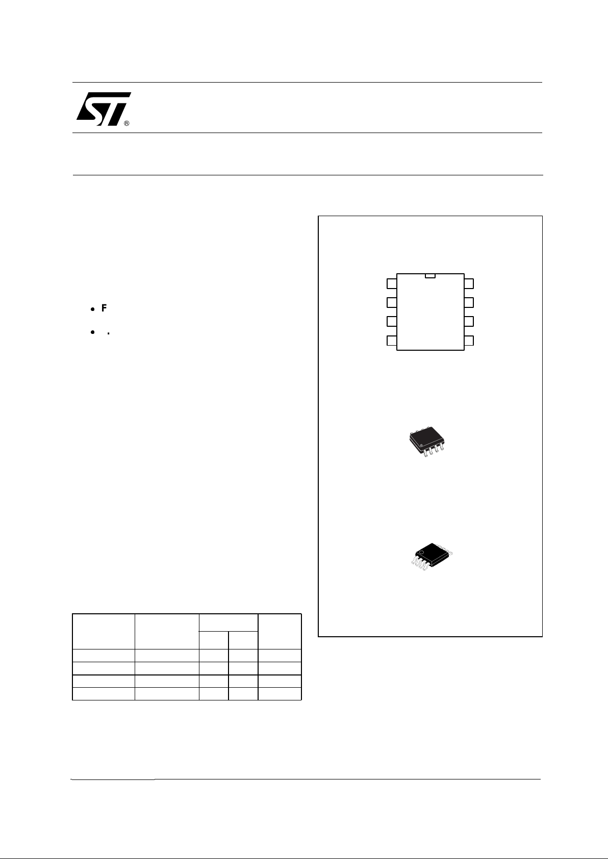
D = Small Outline Package (SO) - also available in Tape & Reel (DT
ST = Small Outline Package (MiniSO8) only available in Tape & Reel
PIN CONNECTIONS (top view)
Part Number
Temperature
Range
Package
Marking
SD
TSM1011ID 0 to 105°C • M1011
TSM1011AID 0 to 105°C • M1011A
TSM1011IS 0 to 105°C • M802
TSM1011AIS 0 to 105°C • M803
1
2
3
45
6
Cc-
Gnd
VccVref
Out 7
8
Cc+
Cv+Cv-
D
SO-8
(Plastic Package)
D
MiniSO-8
(Plastic Micropackage)
TSM1011
Constant Voltage and Constant Current Controller
for Battery Chargers and Adapters
September 2003
TSM1011 PIN DESCRIPTIONS
2/9
1 PIN DESCRIPTIONS
SO8 & MiniSO8 Pinout
2 ABSOLUTE MAXIMUM RATINGS
3 OPERATING CONDITIONS
Name Pin # Type Function
Vref 1 Analog Output Voltage Reference
Cc- 2 Analog Input Input pin of the operational amplifier
Cc+ 3 Analog Input Input pin of the operational amplifier
Cv- 4 Analog Input Input pin of the operational amplifier
Cv+ 5 Analog Input Input pin of the operational amplifier
Gnd 6 Power Supply Ground Line. 0V Reference For All Voltages
Out 7 Analog Output Output of the two operational amplifier
Vcc 8 Power Supply Power supply line.
Symbol DC Supply Voltage Value Unit
Vcc DC Supply Voltage (50mA =< Icc) -0.3V to Vz V
Vi Input Voltage -0.3 to Vcc V
PT Power dissipation W
Toper Operational temperature 0 to 105 °C
Tstg Storage temperature -55 to 150 °C
Tj Junction temperature 150 °C
Iref Voltage reference output current 10 mA
ESD Electrostatic Discharge 2 KV
Rthja Thermal Resistance Junction to Ambient Mini SO8 package 180 °C/W
Rthja Thermal Resistance Junction to Ambient SO8 package
175
°C/W
Symbol Parameter Value Unit
Vcc DC Supply Conditions 4.5 to Vz V
ELECTRICAL CHARACTERISTICS TSM1011
3/9
4 ELECTRICAL CHARACTERISTICS
T
amb
= 25°C and Vcc = +18V (unless otherwise specified)
Symbol Parameter Test Condition Min Typ Max Unit
Total Current Consumption
Icc Total Supply Current, excluding current
in Voltage Reference.
Vcc = 18V, no load
Tmin. < Tamb < Tmax.
1mA
Vz Vcc clamp voltage Icc = 50mA 28 V
Operators
V
io
Input Offset Voltage
TSM1011
TSM1011A
T
amb
= 25°C
T
min.
≤ T
amb
≤ T
max.
T
amb
= 25°C
T
min.
≤ T
amb
≤ T
max.
1
0.5
4
5
2
3
mV
DV
io
Input Offset Voltage Drift 7
µ
V/°C
I
io
Input Offset Current T
amb
= 25°C
T
min.
≤ T
amb
≤ T
max.
23050nA
I
ib
Input Bias Current T
amb
= 25°C
T
min.
≤ T
amb
≤ T
max.
20
50
150
200
nA
SVR Supply Voltage Rejection Ratio V
CC
= 4.5V to 28V 65 100 dB
Vicm Input Common Mode Voltage Range for CV op-amp 1.5 Vcc-1.5 V
Vicm Input Common Mode Voltage Range for CC op-amp 0 Vcc-1.5 V
CMR Common Mode Rejection Ratio T
amb
= 25°C
T
min.
≤ T
amb
≤ T
max.
70
60
85 dB
Output stage
Gm Transconduction Gain. Sink Current
Only
1
1) The cur rent depend s on the difference voltage bewee n the negati ve and the positive input s of the amp l i fier. If the voltage on the minus
input is 1mV higher than the positive amplifier, the sinking current at the output OUT will be increased by 3.5mA.
T
amb
= 25°C
T
min.
≤ T
amb
≤ T
max.
1 3.5
2.5
mA/mV
Vol Low level output voltage at 10 mA
sinking current
200 600 mV
Ios Output Short Circuit Current. Output to
Vcc. Sink Current Only
T
amb
= 25°C
T
min.
≤ T
amb
≤ T
max.
27 50 mA
Voltage reference
V
ref
Reference Input Voltage, Iload=1mA
TSM1011 1% precision
TSM1011A 0.5% precision
T
amb
= 25°C
2.519
2.532
2.545
2.545
2.57
2.557
V
∆
V
ref
Reference Input Voltage Deviation Over
Temperature Range T
min.
≤ T
amb
≤ T
max.
20 30 mV
RegLine Reference input voltage deviation over
Vcc range.
Iload = 5mA 20 mV
RegLoad Reference input voltage deviation over
output current.
Vcc = 18V,
0 < Iload < 10mA
10 mV

TSM1011 ELECTRICAL CHARACTERISTICS
4/9
In the above application sche matic, the TSM1 011 is us ed o n the seco ndary s ide of a f lyback adapter (or
battery charger) to provide an accurate control of voltage and current. The above feedback loop is made
with an optocoupler.
Fig. 1: Inter nal Sche m atic
Fig. 2: Typical Adapter Application Using TSM1011
28V
Vcc
Cv-
Out
GndCc-
Cc+
Cv+
Vref
1
4
5
6
3
2
7
8
CV
CC
D
+
R2
R1
Rsense
Rvc1
22K
Cvc1
2.2nF
Ric1
22K
To primar y
OUT+
OUT-
+
Cic1
2.2nF
Load
IL
Ric2
1K
R5
1K
R4
10K
R3
100
IL
Vsense
28V
Vcc
Cv-
Out
GndCc-
Cc+
Cv+
Vref
1
4
5
6
3
2
7
8
CV
CC
TSM1011

Voltage and Current Control TSM1011
5/9
5 VOLTAGE AND CURRENT CONTROL
5.1 Voltage Control
The voltage loop is controlled via a first
transconductance operational amplifier, the
resistor bridge R
1
, R2, and the optocoupler which
is directly connected to the output.
The relative values of R
1
and R2 should be
chosen in accordance with
Equation 1
:
Equation 1
where V
out
is the desired output voltage.
To avoid discharge of the load, the resistor bridge
R
1
, R2 should have high impedance. For this type
of application, a total value of 100kΩ (or more)
would be appropriate for the resistors R
1
and R2.
For example, if R
2
= 100kΩ, V
out
= 4.10V,
V
ref
=2.5V, then R1 = 41.9KΩ.
Note: If the low drop diode is to be inserted between the
load and the voltage reg ulation resistor bridge to
avoid current flowing from the load through th e
resistor bridge, this drop should be taken into
account in the above calculations by replacing
V
out
by (V
out
+ V
drop
).
5.2 Current control
The current loop is controlled via the second
transconductance operational amplifier, the sense
resistor R
sense
, and the optocoupler.
V
sense
threshold is achieved externally by a
resistor bridge tied t o the V
ref
voltage reference.
Its midpoint is tied to the positive input of the
current control operational amplifier, and its foot is
to be connected to lower potential point of the
sense resistor, as shown in
Figure 3
. The
resistors of this bridge are matched to provide the
best precision possible.
The control equation verifies that:
Equation 2
Equation 2’
where I
lim
is the desired limited current, and
V
sense
is the threshold voltage for the current
control lo op.
Note that the R
sense
resistor should be chosen
taking into account the maximum dissipation
(P
lim
) through it during full load operation.
Equation 3
Therefore, for most adapter and battery charger
applications, a quarter-watt, or half-watt resistor to
make the current sensing function is sufficient.
The current sinking outputs of the two
transconductance operational amplifiers are
common (to the output of the I C). This makes an
ORing function which ensures that whenever t he
current or the voltage reaches too high values, the
optocoupler is activated.
The relation between the controlled current and
the controlled output voltage can be described
with a square characteristic as shown in the
following V/I output-power graph.
Fig. 3 : Output voltage versus output current
R
1
R
2
V
ref
V
out
V
ref
–
---------------------------
⋅
=
R
senseIlim
⋅
V
sense
=
V
sense
R
5
V
ref
R4R
5
+
--------------------⋅=
I
lim
R5V
ref
⋅
R4R
5
+()
R
sense
⋅
------------------------------------------------=
P
lim
V
senseIlim
⋅=
Vout
Iout
Voltage regulation
Current regulation
TSM1011 Vcc : independent power supply
0
Secondary current regulation
TSM1011 Vcc : On power output
Primary current regulation

TSM1011 Compensation
6/9
6 COMPENSATION
The voltage-control transconduc tanc e operat iona l
amplifier can be fully compensated. Both its
output and negative inp ut are directly accessible
for external compensation components.
An example of a suitable compensation network is
shown in
Figure 5
. It consists of a capacitor
C
cv1
=2.2nF and a resistor R
cv1
=22KΩ in series.
The current-control transconductance operationa l
amplifier can be fully compensated. Both of its
output and negative inp ut are directly accessible
for external compensation components.
An example of a suitable compensation network is
shown in
Figure 5
. It consists of a capacitor
C
ic1
=2.2nF and a resistor R
ic1
=22KΩ in serie s .
Fig. 4: Schematic of compensation network
7 START UP AND SHORT CIRCUIT CONDITIONS
Under start-up or short-circuit conditions the
TSM1011 is not provided with a high enough
supply voltage. This is due to the fact that the chip
has its power supply line in common with the
power supply line of the system.
Therefore, the current limitation can only be
ensured by the primary PWM module, which
should be chosen accordingly.
If the primary current limitation is not considered
to be precise enough for the application, then a
sufficient supply for the TSM1011 has to be
ensured under all conditions. This means that it is
necessary to add some circuitry to supply the chip
with a separate power line. This can be achieved
in numerous ways, including an additional winding
on the transformer.
+
CS
DS
D
R2
R1
Rsense
Rvc1
22K
Cvc1
2.2nF
Ric1
22K
To primar y
OUT+
OUT-
+
Cic1
2.2nF
Load
IL
Ric2
1K
R5
1K
R4
10K
R3
100
IL
Vsense
+
Rlimit
Vcc
28V
Vcc
Cv-
Out
GndCc-
Cc+
Cv+
Vref
1
4
5
6
3
2
7
8
CV
CC
TSM1011

Voltage clamp TSM1011
7/9
8 VOLTAGE CLAMP
The schematic in
Figure 5
shows how to realize a
low-cost power supply f or the TSM1011 (with no
additional windings).
Please pay attention to the fact that in the
particular case presented here, this low-cost
power supply can reach voltages as high as twice
the voltage of the regulated line.
Since the Absolute Maximum Rating of the
TSM1011 supply voltage is 28V. In the aim to
protect he TSM1011 against such how voltage
values a internal zener clamp is integrated.
Fig. 5: Clamp voltage
R
limitIvzVccVz
–()⋅=
Vz
28V
Vcc
Rlimit
Vcc
Ivz
TSM1011

TSM1011 PACKAGE MECHANICAL DATA
8/9
9 PACKAGE MECHANICAL DATA
DIM.
mm. inch
MIN. TYP MAX. MIN. TYP. MAX.
A 1.35 1.75 0.053 0.069
A1 0.10 0.25 0.04 0.010
A2 1.10 1.65 0.043 0.065
B 0.33 0.51 0.013 0.020
C 0.19 0.25 0.007 0.010
D 4.80 5.00 0.189 0.197
E 3.80 4.00 0.150 0.157
e 1.27 0.050
H 5.80 6.20 0.228 0.244
h 0.25 0.50 0.010 0.020
L 0.40 1.27 0.016 0.050
k ˚ (max.)
ddd 0.1 0.04
SO-8 MECHANICAL DATA
0016023/C
8

PACKAGE MECHANICAL DATA TSM1011
9/9
10 PACKAGE MECHANICAL DATA
Informat ion furnished is believed t o be accurate and reliable. H owever, STMicr oelectroni cs assumes no responsibility for the
consequences of use of such information nor for any infringement of patents or other rights of third parties which may result from
its use. No license is granted by implication or otherwise under any patent or patent rights of STMicroelectronics. Specifications
mentioned in this publication are subject to change without notice. This publication superse des and replaces all information
previously supplied. STMicroelectr onics products are not au thorized for use as critical c omponents in life support dev ices or
systems without express written approval of STMicroelectronics.
The ST logo is a registered trademark of STMicroelectronics
All other names are the p ro p erty of thei r respective ow ners.
© 2003 STM icroelectronics - All Rights Reser ved
STMicroele ctronics GROUP OF COMPANIES
Australi a - Belgium - B razil - Canada - China - Czech Repubic - Fi nl and - France - Germany
Hong Kong - India - Isr ael - I taly - Japan - Mal aysia - Malt a - M orocco - Sin gapore - Spain
Sweden - Sw itzerland - United Kingdom - Unite d St at es
http://www.st.com
 Loading...