

1/5
OPERATIONAL AMPLIFIER
■LOW INPUT OFFSET VOLTAGE : 0.5mV typ.
■MEDIUM BANDWIDTH (unity gain) : 0.9MHz
■LARGE OUTPUT VOLTAGE SW ING : 0V t o
(VCC - 1.5V)
■INPUT COMMON MODE VOLTAGE RANGE
INCLUDES GROUND
■WIDE POWER SUPPLY RANGE : 5 to 30V
±2.5 TO ±15V
■ESD P R O TECTION : 2kV
COMPARATOR (OPEN COLLECTOR)
■INPUT COMMON MODE VOLTAGE RANGE
INCLUDES GROUND
■LOW OUTPUT SATURATION VOLTAGE :
250mV @ Io = 4mA
DESCRIPTION
The TSM100 is a m onolithic IC that includes o ne
independent op-amp and one in dependent comparator. This device is offering space and cost
saving in many applications like power supply
management or data acquisition systems.
ORDER CODE
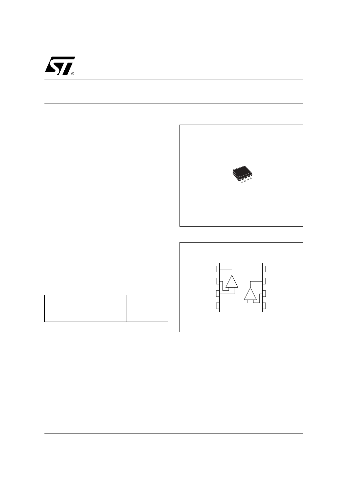
D = Small Outline Package (SO) - also available in Tape & Reel (DT)
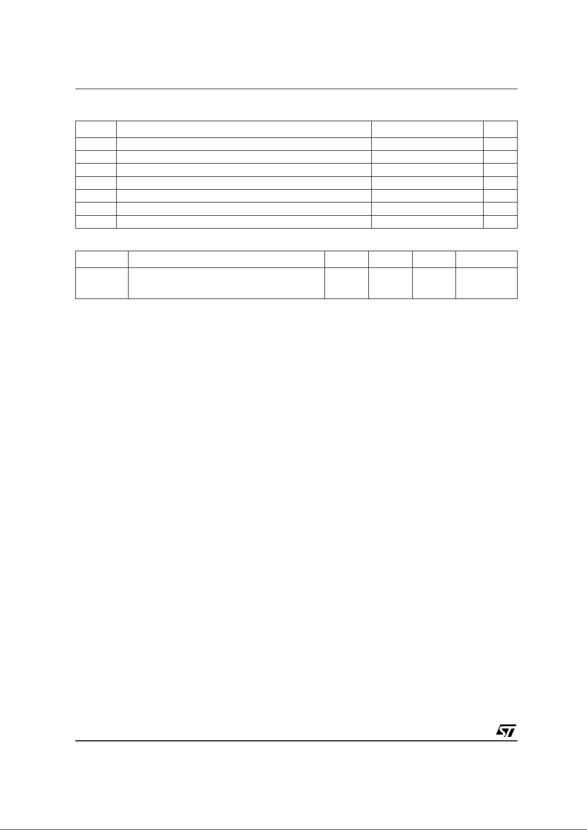
PIN CONNECTIONS (top view)
Part Number
Temperature
Range
Package
D
TSM100I -40°C, +105°C
•
D
SO8
(Plastic Micropacka ge)
+
-
+
-
Amp Output : 1
Amp Input - : 2
Amp Input + : 3
Ground : 4
5 : Comp Input
+
6 : Comp Input -
7 : Comp Output
8 : Vcc
TSM100
SINGLE OPERATIONAL AMPLIFIER AND
SINGLE COMPARATOR
July 2001
TSM100
2/5
ABSOLUTE MAXIMUM RATINGS
ELECTRICAL CHARACTERISTICS
Symbol Parameter Value Unit
V
CC
Supply Voltage 32 V
V
id
Differential Input Voltage 32 V
V
i
Input Voltage -03. to +32 V
T
oper
Operating Free-air Temperature Range -40 to +105 °C
T
j
Maximum Junction Temperature 150 °C
T
l
Maximum Lead Temperature (10 seconds maximum) 260 °C
R
thja
Thermal Resistance Junction to Ambient 175 °C/W
Symbol Parameter Min. Typ. Max. Unit
I
CC
Total Supply Current
Vcc+ = 5V, no load
Vcc+ = 30V, no load
0.9 1.4
1.8
mA

TSM100
3/5
OPERATIONAL AMPLIFIER
V
CC
+
= +5V, VCC = Ground, Vo = 1.4V,T
amb
= 25°C (unless otherwise specified)
Symbol Parameter Min. Typ. Max. Unit
V
io
Input Offset Voltage
T
amb
= 25°C
T
min.
≤ T
amb
≤ T
max.
0.5 3
4
mV
DV
io
Input Offset Voltage Drift 7
µ
V/°C
I
io
Input Offset Current 2 30 nA
I
ib
Input Bias Current 20 150 nA
Avd Large Signal Voltage Gain
V
CC
= 15V, RL = 2k, Vo = 1.4V to 11.4V 50 100
V/mV
SVR Supply Voltage Rejection Ratio
V
CC
= 5V to 30V 65 100
dB
Vicm Input Common Mode Voltage Range
V
CC
= +30V - see note
1)
1. The input common-mode voltage of either input signal voltage should not be allowed to go negative by more than 0.3V. The upper end of
the common-mode voltage range is V
CC
+
- 1.5V.
But both inpu ts can go to Vcc+ +0.3V w i th out damage.
0(V
CC
+
) -1.5
V
CMR Common Mode Rejection Ratio 65 85 dB
I
source
Output Current Source
V
CC
= +15V, Vo = 2V, Vid = +1V 20 40
mA
I
o
Short Circuit to Ground
V
CC
= +15V 40 60
mA
I
sink
Output Current Sink
V
id
= -1V,
V
CC
= +15V, Vo = 2V
V
CC
= +15V, Vo = 0.2V
10
12
20
50
mA
µA
V
OH
High Level Output Voltage
V
CC
+
= 30V
T
amb
= 25°C, RL = 2k
T
amb
= 25°C, RL = 10k
26
27
27
28
V
V
OL
Low Level Output Voltage
R
L
= 10k 5 15
mV
SR Slew Rate at Unity Gain
V
i
= 0.5 to 3V, VCC = 15V
R
L
= 2k, CL = 100pF, unity gain
0.2 0.4
V/µs
GBP Gain Bandwidth Product
V
CC
= 30V,RL = 2k, CL = 100pF
f = 100kHz, V
in
= 10mV
0.5 0.9
MHz
THD Total Harmonic Distortion
f = 1kHz
A
V
= 20dB,RL = 2k, VCC = 30V
C
L
= 100pF, Vo = 2V
pp
0.015
%
e
n
Equivalent Input Noise Voltage
f = 1kHz, Rs = 100
Ω
Vcc = 30V
40
nV/√Hz

TSM100
4/5
COMPARATOR
V
CC
+
= +5V, VCC = Ground,T
amb
= 25°C (unless otherwise specified)
Symbol Parameter Min. Typ. Max. Unit
V
io
Input Offset Voltage
T
amb
= 25°C
15mV
I
io
Input Offset Current 5 50 nA
I
ib
Input Bias Current 25 250 nA
Avd Large Signal Voltage Gain
V
CC
= 15V, RL = 15k, Vo = 1V to 11V 200
V/mV
Vicm
Input Common Mode Voltage Range
1)
1. The input common-mode voltage of either input signal voltage should not be allowed to go negative by more than 0.3V. The upper end of
the common-mode voltage range is V
CC
+
- 1.5V.
But either of both inputs can go to 36V wi t h out damage.
0(V
CC
+
) -1.5 V
I
sink
Output Sink Current
V
id
= -1V, Vo = 1.5V
616 mA
V
OL
Low Level Output Voltage
V
id
= -1V, I
sink
= 4mA 250 400
mV
I
OH
High Level Output Current
V
id
= 1V, Vcc = Vo = 30V 0.1
nA
t
re
Response Time
R
L
= 5.1k to VCC+
2)
2. The respon se time is specifi ed for a 100mV input step with 5mV overdrive. For l arger overdrive signals, 300ns can be obtained
1.3
µs
t
rel
Large Signal Response Time
V
i
= TTL, V
ref
= +1.4V, RL = 5.1k to VCC+
300
ns

TSM100
5/5
PACKAGE MECHANICAL DATA
8 PINS - PLASTIC MICROPACKAGE (SO)
Dim.
Millimeters Inches
Min. Typ. Max. Min. Typ. Max.
A 1.75 0.069
a1 0.1 0.25 0.004 0.010
a2 1.65 0.065
a3 0.65 0.85 0.026 0.033
b 0.35 0.48 0.014 0.019
b1 0.19 0.25 0.007 0.010
C 0.25 0.5 0.010 0.020
c1 45° (typ.)
D 4.8 5.0 0.189 0.197
E 5.8 6.2 0.228 0.244
e 1.27 0.050
e3 3.81 0.150
F 3.8 4.0 0.150 0.157
L 0.4 1.27 0.016 0.050
M 0.6 0.024
S 8° (max.)
Information furnished is believed to be accurate and reliable. However, STMicroelectronics assumes no responsibility for the consequences
of use of su ch i n for mat i on n or f or a ny in fr ing em ent o f pa te nts or ot her r igh ts of th ir d pa r tie s w hic h may res ul t f rom i ts us e. No license is granted
by impl i cation or othe rwise under any patent o r patent right s of STMicroelectronics. Specificat i ons mentioned i n this public ation are subject
to change without notice. T hi s publication supersedes and replaces all informat i on previously supplied. STMicroelectronics products are not
authori zed for use as critical componen ts i n l i fe support devices or systems without express w ri tten approva l of ST M i croelectronics.
© The ST logo is a registered trademark of STMicroelectronics
© 2001 STMicroelectronics - Printed in Italy - All Rights Reserved
STMicr oelectronics GROUP OF COMPANIE S
Australi a - Brazil - China - Finland - Fra nce - Germany - Hong Kong - India - It al y - Japan - Malay si a - Malta - Moro cc o
Singapo re - Spain - Sweden - Switzerland - United Ki ngdom
© http://www.st.com
 Loading...