

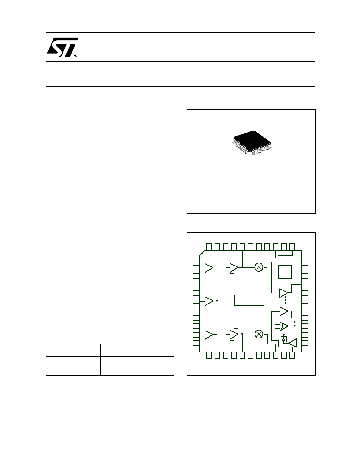
TSH511
TSH511
HiFi stereo/mono infrared receiver
Stereo sub-carrier demodulator
■ Supply voltage: 2.3V to 5.5V
■ Carriers frequency range: 0.4 to 11 MHz
■ Two FM receivers for stereo
■ Integrated audio buffers
■ Audio out puts: 20 mW into 16 ohms
■ High sensitivity: 4µV @12dB SINAD
■ Flexib ilit y : ac c e s s pin s f or each s ec ti o n
■ Receiver 2 Standby for mono operation
DESCRIPTION
The TSH511 is a 0.4 to 11 MHz dual FM receiver.
This circuit offers the functions needed for a highly
sensitive infrared HiFi STEREO receiver.
Featuring high inpu t sensitivity a nd high i nput dynamic range, each receiver integrates a RF
front-end LNA, an intermediate amplifier with 2 external filters, a voltage limiter, a quadrature FM demodulator, and finally an audio buffer.
The integrated audio buffers are abl e to drive directly a 16 ohms headphone with 20mW.
A SQUELCH circuit mutes both audio amplifiers.
Access pins to each section makes the TSH511
suited for a wide field of applications.
For MONO applications, the STANDBY pin enables one receiver only, reducing the supp ly current.
The TSH511 forms a chipset with the du al transmitter TSH512.
APPLICATIONS
■ Infrared HiFi stereo receiver
■ Infrared Multimedia Headsets
■ Stereo sub-carrier demodulator
■ FM IF receiver systems
■ Power Line Carrier Intercoms
ORDER CODE
Part Number
TSH511CF -40°C to
TSH511CFT -40°C to
Temperature
Range
+85°C
+85°C
Package Conditionning Marking
TQFP44 Tray TSH511C
TQFP44 Tape & reel TSH511C
PACKAGE
F
TQFP44
10 x 10 mm
PIN CONNECTION (top view)
424344
424344
1
1
2
2
3
3
4
4
5
5
LNA
LNA
6
6
7
7
8
8
9
9
amp.
amp.
10
10
11
11
12 13 14 15 16 17 18 19 20 21 22
12 13 14 15 16 17 18 19 20 21 22
limiteramp.
limiteramp.
limiter
limiter
FM demodulator
FM demodulator
RX2
RX2
TSH511
TSH511
RX1
RX1
FM demodulator
FM demodulator
36
36
Vref
Vref
Standby
Standby
SQUELCH
SQUELCH
3435
3435
33
33
32
32
31
31
30
30
29
29
28
28
27
27
26
26
25
25
24
24
23
23
3738394041
3738394041
Audio
Audio
buffers
buffers
December 2002
1/18

TSH511
ABSOLUTE MAXIMUM RATINGS
Symbol Parameter Value Unit
Vcc
Supply voltage
Toper Operating free air temperature range -40 to +85 °C
Tstg Storage temperature -65 to +150 °C
Tj Maximum junction temperature 150 °C
Rthjc Thermal resistance juncti on to case 14 °C/W
ESD
except
for pin 6
HBM: Human Body Model
CDM: Charged Device Model
MM: Machine Model
HBM: Human Body Model
ESD
only
for pin 6
CDM: Charged Device Model
MM: Machine Model
Latch-up
1. All voltages values, except differential vol tage, are wit h respect to network gr ound terminal
2. ElectroS tatic Disch arge pulse (E SD pulse) sim ul ating a human body discharge of 10 0 pF through 1.5k
3. Discharge to Ground of a device that has been previously charged.
4. ElectroS tatic Disch arge pulse (E SD pulse) approximati ng a pulse of a ma chine or mec hanical equi pment.
5. Corporate ST Microelectr oni cs proced ure number 0018695
Class
5)
1)
2)
3)
4)
7V
2
1.5
0.2
1
1
0.1
A
Ω
kV
kV
OPERATING CONDITIONS
Symbol Parameter Value Unit
Vcc Supply voltage 2.3 to 5.5 V
f
audio
f
carrier
BLOC DIAGRAM
Audio frequency range 20 to 20,000 Hz
Carrier frequency range 0.4 to 11 MHz
BUF-IN2
MIX-OUT2
MIX-OUT2
Standby
Standby
GND
GND
3435363738
3435363738
SQUELCH
SQUELCH
BUF-IN2
GND
GND
33
33
32
32
SBY1
SBY1
SBY2
SBY2
31
31
30
30
BUF-OUT2
BUF-OUT2
29
29
VCC
VCC
28
28
DEC-OUT
DEC-OUT
27
27
GND
GND
26
26
BUF-OUT1
BUF-OUT1
25
25
MUTE-OUT
MUTE-OUT
24
24
MUTE-INT
MUTE-INT
23
23
MUTE-IN
MUTE-IN
GND
GND
AMP-I N2
AMP-I N2
VCC
VCC
LNA-OUT2
LNA-OUT2
VCC
VCC
LNA-IN
LNA-IN
GND
GND
LNA-OUT1
LNA-OUT1
VCC
VCC
AMP-I N1
AMP-I N1
DEC-LNA
DEC-LNA
DEC-LIM2B
GND
GND
LIM-IN2
LIM-IN2
424344
424344
limiteramp.
limiteramp.
limiter
limiter
DEC-LIM2B
40
40
41
41
RX2
RX2
TSH511
TSH511
RX1
RX1
AMP-OUT2
AMP-OUT2
1
1
2
2
3
3
4
4
5
5
LNA
LNA
6
6
7
7
8
8
9
9
amp.
amp.
10
10
11
11
LIM-OUT2
LIM-OUT2
DEC-LIM2A
DEC-LIM2A
39
39
FM demodulator
FM demodulator
FM demodulator
FM demodulator
MIX-IN2
MIX-IN2
VCC
VCC
Audio
Audio
buffers
buffers
Vref
Vref
2/18
12 13 14 15 16 17 18 19 20 21 22
12 13 14 15 16 17 18 19 20 21 22
MIX-IN1
MIX-IN1
DEC-LIM1B
LIM-IN1
LIM-IN1
AMP-OUT1
GND
AMP-OUT1
GND
DEC-LIM1B
VCC
VCC
MIX-OUT1
GND
MIX-OUT1
DEC-LIM1
LIM-OUT1
DEC-LIM1
LIM-OUT1
GND
BUF-IN1
BUF-IN1
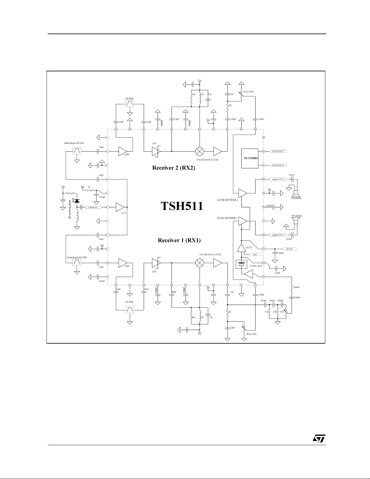
PIN DESCRIPTION
TSH511
Pin Pin name related to
1 GND - - GROUND
2 AMP-IN2 RX2 I Intermediate amplifier input
3 VCC - - SUPPLY VOLTAGE
4 LNA-OUT2 RX2 O Low Noise Amplifier output
5 VCC - - SUPPLY VOLTAGE
6 LNA-IN RX1 & RX2 I Low Noise Amplifier input
7 GND - - GROUND
8 LNA-OUT1 RX1 O Low Noise Amplifier output
9 VCC - - SUPPLY VOLTAGE
10 AMP-IN1 RX1 I Intermediate amplifier input
11 DEC-LNA RX1 & RX2 - Decoupling capacitor
12 AMP-OUT1 RX1 O Intermediate amplifier input
13 GND - - GROUND
14 LIM-IN1 RX1 I Limiter input
15 DEC-LIM1A RX1 - Decoupling capacitor
16 LIM-OUT1 RX1 O Limiter output
17 DEC-LIM1B RX1 - Decoupling capacitor
18 MIX-IN1 RX1 I Mixer input
19 VCC - - SUPPLY VOLTAGE
20 MIX-OUT1 RX1 O Mixer output (demodulated audio signal)
21 GND - - GROUND
22 BUF-IN1 RX1 I Audio buffer input
23 MUTE-IN RX1 & RX2 I Noise amplifier input (Squelch circuit)
24 MUTE-INT RX1 & RX2 - Capacitor connection of the noise rectifier
25 MUTE-OUT RX1 & RX2 O Capacitor connection (ramp generator to mute the audio)
26 BUF-OUT1 RX1 O Audio buffer output
27 GND - - GROUND
28 DEC-OUT RX1 & RX2 - Decoupling capacitor of Audio buffers
29 VCC - - SUPPLY VOLTAGE
30 BUF-OUT2 RX2 O Audio buffer output
31 SBY2 RX1 & RX2 I Standby 2
32 SBY1 RX1 & RX2 I Standby 1
33 GND - - GROUND
34 BUF-IN2 RX2 I Audio buffer input
35 GND - - GROUND
36 MIX-OUT2 RX2 O Mixer output
37 VCC - - SUPPLY VOLTAGE
38 MIX-IN2 RX2 I Mixer input
39 DEC-LIM2A RX2 - Decoupling capacitor
40 LIM-OUT2 RX2 O Limiter output
41 DEC-LIM2B RX2 - Decoupling capacitor
42 LIM-IN2 RX2 I Limiter input
43 GND - - GROUND
44 AMP-OUT2 RX2 O Intermediate amplifier output
1. pin direction: I = inp ut pin, O = output pi n, - = pi n to connect to supply or deco upl i ng capacitors or external compo nents
direction
1)
Pin description
3/18
TSH511
TYPICAL SCHEMATIC
Stereo infrared receiver
4/18
TSH511
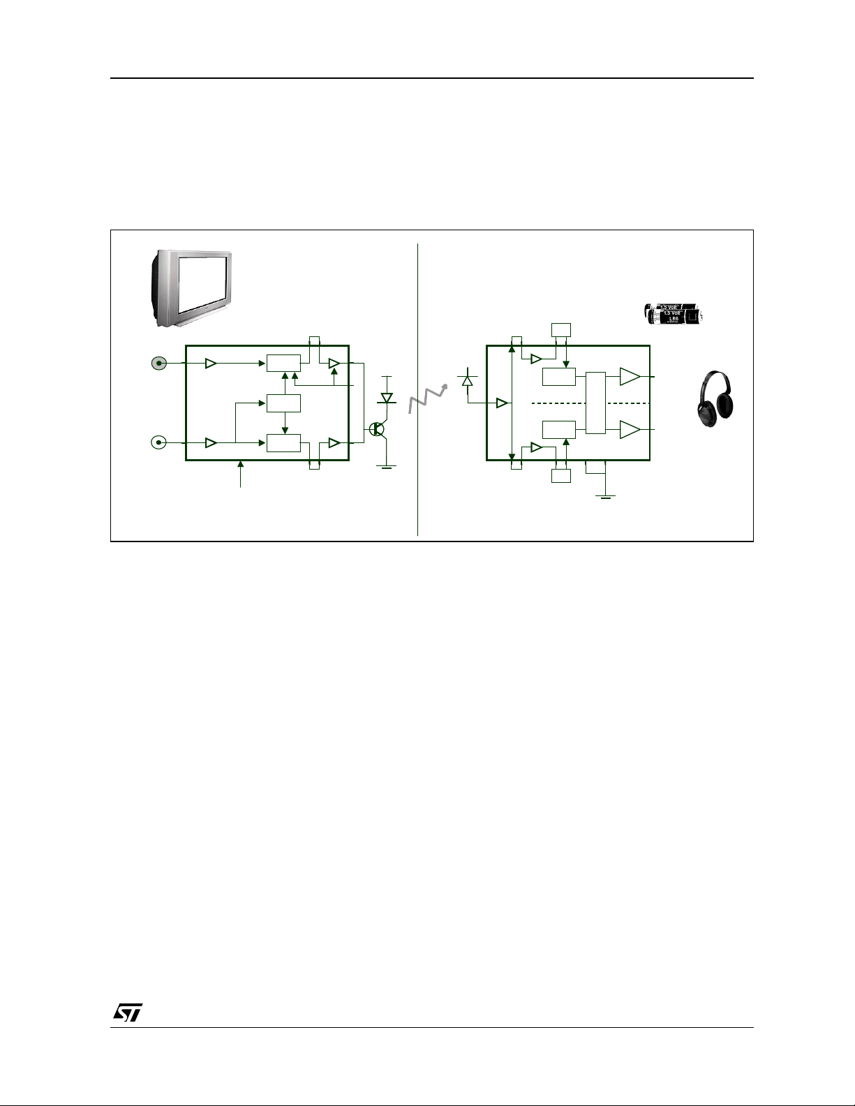
INFRARED STEREO HEADPHONE APPLICATION
The right side of the figure shows the block-diagram of an infrared stereo receiver using the TSH511. The
sensitive LNA directly connected to the photodiode does not require an external pre-amplifier. After filtering, the amplified signals are limited and demodulated with quadrature demodulators. The two integrated
audio buffers directly drive the stereo headphones. The aud io power reaches 2
The built-in squelch function fades-out the audio when the incoming infrared signal is low. The standby inputs SBY1 and SBY2 enable only one receiver for the mono applications.
x20mW in two 16Ω loads.
Right
Right
channel
channel
Line inputs
Line inputs
Left
Left
channel
channel
LNA + ALC
LNA + ALC
LNA + ALC
LNA + ALC
Power supply:
Power supply:
2.3 to 5.5V
2.3 to 5.5V
Icc < 20 mA stereo
Icc < 20 mA stereo
IR stereo HiFi transmitter
IR stereo HiFi transmitter
(Television)
(Television)
TSH512 TSH511
TSH512 TSH511
buffer2
TX2
TX2
VOX
VOX
TX1
TX1
buffer2
buffer1
buffer1
SBY
SBY
Vcc
Vcc
LED
LED
F
F
i
i
H
H
.
.
2
2
photodiode
photodiode
:
:
o
o
z
z
e
e
r
r
H
H
e
e
t
t
M
M
s
s
i
i
8
8
.
.
2
2
&
&
3
3
IR stereo HiFi receiver
IR stereo HiFi receiver
(Headphones)
(Headphones)
LNA
LNA
s
s
r
r
e
e
i
i
r
r
r
r
a
a
c
c
2.3 MHz
2.3 MHz
filter
filter
RX2
RX2
RX1
RX1
filter
filter
2.8 MHz
2.8 MHz
SQUELCH
SQUELCHSQUELCH
SBY1
SBY1
SBY2
SBY2
Vcc: 2.3 to 5.5V
Vcc: 2.3 to 5.5V
Current < 15 m A
Current < 15 m A
Audio
Audio
buffer2
buffer2
Audio
Audio
buffer1
buffer1
20 mW / 16 Ω
20 mW / 16 Ω
20 mW / 16 Ω
20 mW / 16 Ω
5/18

TSH511
MULTIMEDIA APPLICATION: HEADSET SIDE
The TSH511 recei ves the HiFi stereo sound f rom th e com pute r throu gh 2.3 and 2.8 MHz stereo infrared
carriers. The access pins to the RF amplifiers allow the use of a 1.7 M H z reject filter to c ancel the t ransmitted signal of the microphone. The wide supply range (2.3 to 5.5 V) allows battery operation.
TSH511 & 512 supply:
TSH511 & 512 supply:
TSH511 & 512 supply:
2.3 to 5.5V, 25 mA
2.3 to 5.5V, 25 mA
2.3 to 5.5V, 25 mA
Voice transmittedto the PC
Voice transmittedto the PC
Voice transmittedto the PC
TSH512
TSH512
TSH512
LNA + ALC
LNA + ALC
LNA + ALC
MIC. BIAS
MIC. BIAS
MIC. BIAS
MIC. BIAS
MIC. BIAS
MIC. BIAS
LNA + ALC
LNA + ALC
LNA + ALC
TX2
TX2
TX2
VOX
VOX
VOX
TX1
TX1
TX1
1.7 MHz
1.7 MHz
1.7 MHz
Band-pass
Band-pass
Band-pass
filter
filter
filter
buffer2
buffer2
buffer2
buffer1
buffer1
buffer1
SBY
SBY
SBY
HiFi stereofromthe PC:
HiFi stereofromthe PC:
HiFi stereofromthe PC:
2x 20 mW /16 Ω
2x 20 mW /16 Ω
2x 20 mW /16 Ω
Vcc
Vcc
Vcc
Vcc
Vcc
Vcc
LED
LED
LED
TSH511
TSH511
TSH511
Audio
Audio
Audio
buffer2
buffer2
buffer2
Audio
Audio
Audio
buffer1
buffer1
buffer1
1.7 MHz
1.7 MHz
1.7 MHz
reject
reject
reject
filter
filter
filter
RX2
RX2
RX2
SQUELCH
SQUELCH
SQUELCH
RX1
RX1
RX1
SBY1
SBY2
SBY1
SBY2
SBY1
SBY2
filter
filter
filter
1.7 MHz
1.7 MHz
1.7 MHz
reject
reject
reject
Microphone Tx:
Microphone Tx:
Microphone Tx:
1.7 MHz
1.7 MHz
1.7 MHz
carrier
carrier
carrier
2.3 MHz
2.3 MHz
2.3 MHz
Band-pass
Band-pass
Band-pass
filter
filter
filter
filter
filter
filter
2.8 MHz
2.8 MHz
2.8 MHz
Band-pass
Band-pass
Band-pass
LNA
LNA
LNA
Stereo Rx:
Stereo Rx:
Stereo Rx:
2.3 & 2.8 MHz
2.3 & 2.8 MHz
2.3 & 2.8 MHz
photodiode
photodiode
photodiode
MULTIMEDIA APPLICATION: COMPUTER SIDE
In multimedia application, the TSH511 receives the voice of the user through the 1.7 MHz infrared carrier.
The standby pins can disable the unused receiver and audio amplifier to reduce the supply current.
TSH511 & 512 supply:
TSH511 & 512 supply:
2.3 to 5.5V, 24 mA
2.3 to 5.5V, 24 mA
Voice from the headset microphoneHiFi stereo
mono Rx:
mono Rx:
1.7 MHz
1.7 MHz
HiFi stereo Tx:
HiFi stereo Tx:
2.3 & 2.8 MHz
2.3 & 2.8 MHz
LED
LED
buffer2
buffer2
SBY
SBY
buffer1
buffer1
TX2
TX2
VOX
VOX
TX1
TX1
TSH512
TSH512
LNA + ALC
LNA + ALC
LNA + ALC
LNA + ALC
photodiode
photodiode
Voice from the headset microphoneHiFi stereo
LNA
LNA
RX2
RX2
RX1
RX1
filter
filter
1.7 MHz
1.7 MHz
Band-pass
Band-pass
TSH511
TSH511
SQUELCH
SQUELCHSQUELCH
SBY2
SBY2
SBY1
SBY1
Vcc
Vcc
Audio
Audio
buffer2
buffer2
Audio
Audio
buffer 1
buffer 1
6/18

TSH511
ELECTRICAL CHARACTERISTICS
Vcc = 2.7V, Tamb = 25°C, faudio = 1 kHz, fcarrier = 2.8 MHz, frequency deviation = +/-75 kHz (unless
otherwise specified)
Symbol Parameter Test condition Min Typ Max Unit
Overall Circuit (refering to typical application schematic, without reject filters)
I
CC_OX
Current consumption,
RX1 is on, RX2 is on.
Current consumption
I
CC_10
RX1 is on, RX2 is off
RX1 audio buffer is on
RX2 audio buffer is on
Current consumption
I
CC_11
RX1 is on, RX2 is off
RX1 audio buffer is on,
RX2 audio buffer is off
MAUS Maximum Usable Average Sensitivity
SN
V
Output audio signal to noise ratio
OUT
Input limiting voltage
i
THD Total Harmonic Distortion
Low Noise Amplifier (LNA) Section
G
LNA
BW
E
n_LNA
I
n_LNA
Z
LNA_IN
Z
LNA_OUT
P
1dB_LNA
IIP3
LNA voltage gain
-3dB LNA Bandwidth ZL = 2 k
LNA
Equivalent input noise voltage Rs = 0
Equivalent input noise current Rs = 0
Input impedance definied as
R
in paralell with C
LNA_IN
LNA_IN
Output impedance 200
1dB compression point
Input 3rd order interception point
LNA
SBY1 = ’Low’,
SBY2 = X
(X = don’t care)
SBY1 = ’High’,
SBY2 = ’Low’
SBY1 = ’High’,
SBY2 = ’High’
with audio SINAD=12 dB
audio BW=30 kHz
with audio SINAD=26 dB
audio BW=30 kHz
V
carrier
= 1 mV
RMS
, with
psophometric filter
output S/N reduced by
3dB, in BW = 30kHz
output S/N reduced by
3dB, psophometric filter
V
carrier
= 1 mV
RMS
, with
psophometric filter
ZL= 2 k
Ω,
= 10 MHz
f
carrier
Ω
Ω
Ω
R
LNA_IN
C
LNA_IN
ZL= 2 k
Ω
ZL= 2 k
ZL= 2 k
ZL= 2 k
Ω,
Ω
Ω,
f
carrier
f
carrier
=10 MHz
=10 MHz
15 18 mA
11 13 mA
9.5 11.5 mA
,
4
,
19
58 dB
80
60
0.6 %
18 22 28 dB
20 MHz
3.4 nV/√Hz
0.6 pA/√Hz
30
2
127
95
30
22
µV
µV
mV
mV
RMS
RMS
k
Ω
pF
Ω
RMS
RMS
7/18

TSH511
Symbol Parameter Test condition Min Typ Max Unit
Amplifier (AMP) Section
G
AMP
Z
AMP_IN
Z
AMP_OUT
P
1dBAMP
BW
Amplifier Voltage Gain
Input impedance defined as
R
in parallel with C
AMP_IN
Output impedance 350
1dB compression point
-3dB AMP Bandwidth ZL = 2 k
AMP
Limitor (LIM) Section
G
Z
LIM_IN
V
LIM_OUT
Voltage gain ZL=15kΩ tied to GND 50 54 60 dB
LIM
Input impedance defined as
R
in parallel with C
LIM_IN
Output Voltage ZL = 15 kΩ tied to GND 170
FM Demodulator Section
V
DEM
Z
DEM_OUT
Output voltage
Output impedance 100
Squelch Section
ATT
Z
N_IN
V
N_TH
V
N_HYS
Audio attenuation on each receiver
when audio buffers are muted.
Noise Amplifier Input impedance 2 k
Comparator threshold
Comparator hysteresis
Current sinked on pin 25 to discharge
capacitor: ramp generator con-
C
I
MUTE_SINK
MUTE
trolling the attenuation from ON to OFF
states of audio buffers.
Current sourced on pin 25 to charge
C
I
MUTE_SOU
RCE
capacitor: ramp generator con-
MUTE
trolling the attenuation from OFF to ON
states of audio buffers.
AMP_IN
LIM_IN
ZL=2 k
Ω,
R
AMP_IN
C
AMP_IN
ZL = 2 k
ZL = 2 k
=10 MHz
f
carrier
R
LIM_IN
C
LIM_IN
+-75 kHz FM deviation
typical a ppl i cation sch em atic
ZL = 4 k
RX1 and RX2 audio buffers muted
ZL = 16 Ω on both audio
buffers
from MUTED to
UNMUTED state,
R
= 22 k
MUTE
f
= 100 kHz
IN
= 22 k
R
MUTE
= 100 kHz
f
IN
Voltage on pin 25 = 1.7V 24 µA
Voltage on pin 25 = 1.7V 14 µA
Ω
Ω,
Ω
Ω
f
carrier
=10 MHz
Ω,
Ω,
16 20 dB
10
2
560
220
380
11 MHz
15
2
700 800 900
55 65 dB
9
1
mV
mV
mV
mV
mV
k
pF
Ω
k
pF
Ω
Ω
RMS
Ω
pp
RMS
Ω
RMS
RMS
8/18

TSH511
Symbol Parameter Test condition Min Typ Max Unit
Audio Buffers
Z
OD-IN
BW
1dB
P
OUT_OD
THD
THD
V
ISOL
Standby
Input Impedance
-1dB bandwith ZL = 16
Output power
Distortion in Line Driver mode
OD
Distortion in Power Amplifier mode
OD
Crosstalk: isolation between the two
Audio Buffers
Ω
ZL= 16
Ω
= 70mV
V
OD_IN
Vout = 0.5 V
= 10kΩ
Z
L
RMS
RMS
,
with decoupling capacitor
CDEC = 1µF/ceramic on
pin 28.
Pout = 20 mW,
ZL = 16Ω
Pout = 20 mW, ZL = 16
15 20 mW
Ω
200 k
35 kHz
0.2 0.3 %
0.35 0.8 %
51 dB
Ω
V
SBY_L
V
SBY_H
T
T
ON
OFF
Low level input voltage of Standby
inputs (Pins 31 & 32)
High level input voltage of Standby
inputs (Pins 31 & 32)
Turn-on time from Standby mode to
Active mode
Turn-off time from Active mode to
Standby mode
0.1
xV
CC
xVcc V
0.9
0.5 µs
0.5 µs
V
9/18

TSH511
OVERALL CIRCUIT
Supply current vs. Supply voltage
Squelc h Th re shold vs. R
Input Resistor
MUTE
20
18
16
14
12
10
(mA)
CC
I
8
6
4
2
0
0123456
RX1+RX2+Buffers
RX1+Buffers
VCC(V)
S/N vs. 2.8 MHz Input Level
60
50
40
30
Total S/N (dB)
20
10
0
1 10 100 1000
PSOPH
Input Level (µV)
RX1+ (RX1 Buffer)
BW = 30 kHz
VCC = 2.7 V
Deviation = +/-75 kHz
60
VCC = 2.7V
50
40
)
RMS
(mV
30
N_TH
V
20
10
FIN = 1 MHz
0
1 10 100
R
MUTE
FIN = 100 kHz
(kΩ)
Supply current vs. Temperature
20
VCC = 2.7V
18
16
14
12
10
(mA)
CC
I
8
6
4
2
0
-40-200 20406080
TX1+TX2+Buffers
TX1
T
(°C)
AMB
TX1+TX2
TX1+Buffers
PSOPH: Signal on Noise Ratio curve measured with a CCITT
standard psophometric bandp ass characteristic. It approximates
the response of human hearing .
10/18
Sensitivity vs. Supply Voltage
25
20
15
10
5
Sensitivity (µV) @ 26 dB SINAD
0
2345
F
F
Deviation = +/- 75kHz
BW = 30 kHz
VCC(V)
CARRIER
= 1 kHz
MOD
= 2.8MHz

AUDIO BUFFERS
Output THD+N vs. Output Power (RL = 16 Ω)
TSH511
Output THD+N vs. Output Power (RL = 16 Ω)
10
VCC = 2.3V
VCC = 2.7V
(%)
BUFFER
1
VCC = 5.5V
THD+N
RL = 16 Ω
F = 1 kHz
0.1
1 10 100
P
OUT-BUF
(mW)
BW = 30 kHz
Output THD+N vs. Output Power (RL = 32 Ω)
10
(%)
THD+N
BUFFER
1
0.1
RL = 32 Ω
F = 1 kHz
BW = 30 kHz
110100
VCC = 2.3V
VCC = 2.7V
P
OUT-BU F
VCC = 5.5V
(mW)
10
F = 20 kHz
(%)
BUFFER
1
THD+N
0.1
F = 1 kHz
RL = 16 Ω
F = 20 Hz
VCC = 2.7 V
110100
P
(mW)
OUT-BU F
Output THD+N vs. Output Power (RL = 32 Ω)
10
F = 20 kHz
(%)
BUFFER
1
0.1
F = 1 kHz
F = 20 Hz
RL = 32 Ω
VCC = 2.7 V
110100
P
(mW)
OUT-BU F
THD+N
Output THD+N vs. Output Power (RL = 600 Ω)
VCC = 2.3V
1
(%)
BUFFER
THD+N
0.1
VCC = 2.7V
VCC = 5.5V
RL = 600 Ω
F = 1 kHz
BW = 30 kHz
0.1 1 10
P
(mW)
OUT-BUF
Output THD+N vs. Output Power (RL = 600 Ω)
10
F = 20 kHz
(%)
BUFFER
1
0.1
F = 20 Hz
F = 1 kHz
0.1 1
P
(mW)
OUT- BUF
RL = 600 Ω
VCC = 2.7 V
11/18
THD+N

TSH511
Output THD+N vs. Output Voltage (RL = 10kΩ)
10
RL = 10 kΩ
F = 1 kHz
BW = 30 kHz
VCC = 2.3V
VCC = 2.7V
(%)
1
BUFFER
VCC = 5.5V
THD+N
0.1
0.1 1
V
OUT-BUF(Vrms
)
Output THD+N vs. Frequency (RL = 16 Ω)
10
VCC = 2.7 V
Vin = 50 mV
RL = 16 Ω
(%)
BUFFER
1
rms
Output THD+N vs. Output V oltage (RL = 10kΩ)
10
RL = 10 kΩ
VCC = 2.7 V
(%)
1
BUFFER
F = 20 Hz
F = 1 kHz
F = 20 kHz
THD+N
0.1
0.1 1
V
OUT-BUF(Vrms
)
Output THD+N vs. Frequency (RL = 32 Ω)
10
VCC = 2.7 V
Vin = 50 mV
RL = 32 Ω
(%)
BUFFER
1
rms
THD+N
0.1
20
100 1000 10000
Frequency (Hz)
Output THD+N vs. Frequency (RL = 600 Ω)
10
VCC = 2.7 V
Vin = 50 mV
RL = 600 Ω
(%)
BUFFER
1
THD+N
0.1
20
rms
100 1000 10000
Frequency (Hz)
THD+N
0.1
20
100 1000 10000
Frequency (Hz)
Output THD+N vs. Frequency (RL = 10 kΩ)
10
VCC = 2.7 V
Vin = 50 mV
RL = 10 kΩ
(%)
BUFFER
1
THD+N
0.1
20
rms
100 1000 10000
Frequency (Hz)
12/18

Output Power vs. Temperature
24
22
20
(mW)
18
OUT-BUF
16
P
14
12
10
-40-200 20406080
T
AMB
VCC = 2.7V
RL = 16 Ω
VIN = 70 mV
(°C)
TSH511
RMS
13/18

TSH511
GENERAL DESCRIPTION
The TSH511 is a 0.4 to 11 MHz dual FM analogue
receiver. The incoming signal is amplified with a
22 dB Low Noise Amplifier (LNA section). The
good noise performance of the LNA allows the
photodiode for infrared applications to be connected directly to the TSH511 without any external
preamplifier. The access pins for each section and
the two standby configurations allow a high versatility for many applications: HiFi stereo infrared receiver, mono/stereo subcarrier receiver, power
line carrier audio.
Figure 1 : TSH511 block diagram
MIX-IN2
LIM-OUT2
LIM-OUT2
DEC-L IM2 A
DEC-L IM2 A
FM demodulator
FM demodulator
RX2
RX2
TSH511
TSH511
RX1
RX1
FM demodulator
FM demodulator
DEC-LIM1B
DEC-LIM1B
LIM-OUT1
LIM-OUT1
MIX-IN2
MIX-IN1
MIX-IN1
GND
GND
AMP-IN2
AMP-IN2
VCC
VCC
LNA-OUT2
LNA-OUT2
VCC
VCC
LNA-IN
LNA-IN
GND
GND
LNA-OUT1
LNA-OUT1
VCC
VCC
AMP-IN1
AMP-IN1
DEC-LNA
DEC-LNA
DEC-L IM2 B
AMP-OUT2
AMP-OUT2
1
1
2
2
3
3
4
4
5
5
LNA
LNA
6
6
7
7
8
8
9
9
amp.
amp.
10
10
11
11
12 13 14 15 16 17 18 19 20 21 22
12 13 14 15 1 6 17 1 8 19 20 21 22
AMP- OUT1
AMP- OUT1
DEC-L IM2 B
GND
LIM-IN2
GND
LIM-IN2
424344
424344
limiteramp.
limiteramp.
limiter
limiter
LIM-IN1
LIM-IN1
DEC-LIM1
DEC-LIM1
GND
GND
BUF-IN2
36
36
Audio
Audio
buffers
buffers
Vref
Vref
MIX-OUT2
MIX-OUT2
MIX-OUT1
MIX-OUT1
Standby
Standby
GND
GND
3435
3435
SQUELCH
SQUELCH
GND
GND
BUF-IN2
33
33
GND
GND
32
32
SBY1
SBY1
31
31
SBY2
SBY2
BUF-OUT2
30
BUF-OUT2
30
29
29
VCC
VCC
28
28
DEC-OUT
DEC-OUT
27
27
GND
GND
26
26
BUF-OUT1
BUF-OUT1
25
25
MUTE-OUT
MUTE-OUT
24
24
MUTE-INT
MUTE-INT
23
23
MUTE-IN
MUTE-IN
BUF-IN1
BUF-IN1
VCC
VCC
3738394041
3738394041
VCC
VCC
The LNA is common to both receivers but the output is split in two: one for each receiver. Each LNA
output can be connected to a first optional filter for
bandpass or reject filtering.
The filtered signal is amplified with an intermediate Amplifier (AMP section) followed by a second
filter. The AMP sections have 20 dB typical gain.
Finally, the sign al is amplified an d limited in the
Limiter (LIM section). The 6 0 dB amplifier-limiter
LIM provides a constant amplitude signal to the
demodulator. It reduces A M parasitics dem odulation in the FM demodulator.
The FM demodulator is a classical quadrature detector using an external tank.
The demodulated s ignal can be amplified by the
Audio Buffer section after de-em phasis. Eac h Audio Buffer can drive a 16 ohms headphone with 20
mW power.
The two standby pins SBY1 & SBY2 allow the second receiver RX2 to be put into standby for mono
operation. In mono, it is possible to use both Audio
Buffers or only one depending on the combination
on SBY1 & SBY2.
To avoid noise at the audio output, a Squelch section mutes the Audio Buffers when no carrier is received. The Squelch Section uses the demodulated signal of the first receiver (RX1). This signal is
highpass filtered, rectified and compared to a
threshold to produce the Mute signal (pin 25).
When no carrier is received on RX1, the wideband
’FM noise’ on the demodulator increases and t he
Mute signal mutes the both Audio Buffers. Wh en
the carrier is present, the wideband noise on the
demodulator output decreases, enabling the Audio Buffers.
Figure 2 : Infrared audio frequencies
IR frequency applications
1.6 MHz AM mono
1.7 MHz FM mono
2.3 MHz FM right channel
2.8 MHz FM left channel or mono
LNA section: Low Noise Amplifier
The Low Noise Amplifier (LNA) has a typical gain
of 22 dB to amplify the incomi ng RF signal from
the photodiode. The LNA is common to both receivers sections RX1 and RX2.
Figure 3 : LNA schematic
14/18

TSH511
The LNA output is directly connected to
LNA-OUT1 and LNA-OUT 2 pins in parallel (pin 8
and 4 respectively). As the LNA minimum impedance load is 1 k
LNA-OUT1 or LNA-OUT2 must be 2 k
The series 50
Ω, the load impedance on each pin
Ω minimum.
Ω resistor and the 100 nF capacitor
decouple the LNA supply voltage (pin 5), improving noise performance.
AMP and LIM sections: Amplifier and Limitor
The first filter output is connected to the intermediate amplifier AMP. The gain of AMP is typically 20
dB. The second filter is connected between the
output of AMP and the input of the limitor LIM. The
60 dB limitor LIM provides a constant amplitude
signal to the FM demodulator. It reduces the AM
parasitic effects into the FM demodulator.
Figure 4 : AMP and LIM schematic
allows to adjustment of the demodula tion characteristic. For a given transmitting deviation, a lower
value of Rlo gives a lower demodulated amplitude
and reduces the distortion.
The AC amplitude on pin 18 must not exceed 300
mV
to prevent clipping by the internal ESD di-
RMS
odes of the circuit.
The low output impedance of the demodulator
(MIX-OUT pins) drives the external volume control
and the de-emphasis filter.
Figure 5 : FM demodulator schematic
FM demodulator section
The FM demodulator is a classical quadrature demodulator based on a multiplier. The quadrature is
performed with the tank circuit Llo inductor and
Clo capacitor. The tank circuit is tuned on the receiving frequency.
The Rlo resist or is connected in p arallel with Llo
and Clo to reduce the Q factor of the tank circuit. It
SQUELCH section
To avoid audio ’FM noise’ at the speakers when
no carrier is received, the TSH511 has a built-in
Squelch circuit. The Squelch detects the wideband ’FM noi se’ on the demodulated output a nd
fades-out the audio of both audio buffers.
The audio is filtered f rom the ’FM noise’ using t he
high-pass RC filter. The cut-off frequency is t ypically 100kHz. T he squelch level depends on t he
value of the R
resistor in serie with the input
MUTE
pin of the noise amplifier MUTE-IN (pin 23). The
detected noise is integrated with the Cpeak capacitor connected to MUTE-INT pin. The DC voltage on this pin follows the amplitude of the noise.
15/18

TSH511
The comparator a nd the C
capacitor gener-
MUTE
ate the fade-in and fade-out control ramps for the
audio buffers. The Squelch has been designed
with particular attention to avoid audio pop-noise.
Figure 6 : Squelch schematic
The Audio Buffers can also drive the other usual
impedances used in audio: 32
Ω, 600Ω and 10kΩ
(see the corresponding distorsion curves).
The high input imped ances of the Audio Buffers
reduce the coupling capacitors to less than 0.1 µF
allowing space and cost saving.
Standby section
Depending on the states of the logic inputs SBY1
and SBY2, RX2 and the Audio Buffer2 can be
disabled separately. The TSH511 receiver can
adapt to different applications by using SBY1 &
SBY2 standby pins:
SBY1
pin 32
SBY2
pin 31
RX1 &
audio
buffer1
RX2
audio
buffer 2
typical
use
Low Low
Low High
ON ON ON
High Low ON OFF ON
High High ON OFF OFF
stereo
mono on
the tw o
outputs
mono on
one output
The squelch section is driven by the receiver RX1
but controls both audio buffers.
Audio Buf fe r sections
The audio signal from a F M demodulator enters
into the 6dB/octave low-pass filter for de-empha-
sis. 50µs and 75µs are standard de-emphasis values.
After the de-emphasis network, the potentiomet er
controls the volume.
The Rail-to-Rail output stage of each Audio Buffer
is able to drive 20 mW into 16
Ω at 2.3V supply
voltage. In this condition, the distortion is typically
0.3% before saturation.
In the standard stereo mode, the configuration is:
SBY1 = SBY2 = ’Low’
In mono mode with one load(example: a single
loadspeaker), RX2 and Audio Buffer 2 are
disabled, the configuration is SBY1 = SBY2 =
’High’.
In mono mode with a stereo load (example: a
stereo headphone), the configuration is SBY1 =
’high’, SBY2 = ’Low’.
A pin connected to Vcc is at ’High’ state, and if
connected to GND is at ’Low’ state.
16/18

TSH511
APPLICA TI ON SCHEMATIC
The infrared carriers are de tected by the photodiod e and the s ignal is directly am plified by the TSH511.
Optional reject filters can be added in each channel to improve crosstalk performances. Each receiver has
a standard bandpass filter (filters F1 & F3) to select the 2.3 and 2.8 MHz carriers. After the FM
demodulators, the potentiometers P1 and P2 control the volume levels. The stereo headphones are
directly connected to the integrated audio buffers. The potentiometer P3 allows adjustment of the
sensitivity of the Sque lch. The Squelch function fade-in an d fade-out the au dio signal depending on the
level of the 2.8 MHz carrier.
17/18

TSH511
PACKAGE MECHANICAL DATA
44 PINS - PLASTIC PACKAGE
44 34
1
A
A2
e
0,10 mm
.004 inch
33
E3
SEATING PLANE
E
E1
A1
B
11
12 22
D3
D1
D
23
L1
c
L
K
0,25 mm
.010 inch
GAGE PLANE
Dimensions Millimeters Inches
Min. Typ. Max. Min. Typ. Max.
A 1.60 0.063
A1 0.05 0.15 0.002 0.006
A2 1.35 1.40 1.45 0.053 0.055 0.057
B 0.30 0.37 0.40 0.012 0.015 0.016
C 0.09 0.20 0.004 0.008
D 12.00 0.472
D1 10.00 0.394
D3 8.00 0.315
e 0.80 0.031
E 12.00 0.472
E1 10.00 0.394
E3 8.00 0.315
L 0.45 0.60 0.75 0.018 0.024 0.030
L1 1.00 0.039
K 0° (min.), 7° (max.)
Information furnished is bel ieved to be accurate and reliable. However, STMicroe lectronics assumes no responsibility for the
consequences of use of such information nor for any infringement of patents or other rights of third parties which may result from
its use. No li cense is granted by i mp lica tion or otherwise under a n y patent or patent rig hts of STMicroelectronics. Spec ific at ions
mentioned in this publication ar e subject to change without notice. This publication supersedes and replaces all information
previously supplied. S TMicroelectronics products are not authorized for use as critica l components in life suppo rt devices or
systems without express written approval of STMicroelectronics.
Australi a - Brazil - C hi na - Finlan d - F rance - Germ any - Hong Kon g - I ndi a - Italy - Japan - Malaysia - Malta - Morocco
The ST logo is a registered trademark of STMicroelectronics
© 2002 STMicroelectronics - All Rights Reserved
STMicr o el ectronics G ROU P OF COMPANI E S
Singapo re - Spain - Sweden - Swi t zerland - United Kingdom
http://www.st.com
18/18
 Loading...