

SGS Thomson Microelectronics TSH321IN, TSH321ID, TSH321D, TSH321 Datasheet
TSH321
WIDE BANDWIDTHAND MOS INPUTS
SINGLE OPERATIONALAMPLIFIER
June 1998
ORDERCODES
Part
Number
Temperature
Range
Package
ND
TSH321I -40
o
C, 125oC ••
321-01.TBL
1
2
3
4
8
6
5
7
Inverting Input
Non-invertingInput
Output
Offset Null 2Offset Null 1
N.C.
V
CC
V
CC
+
321-01.EPS
PINCONNECTIONS (top view)
.LOW DISTORTION
.GAIN BANDWIDTH PRODUCT : 300MHz
.GAIN OF 2 STABILITY
.SLEW RATE : 400V/µs
.VERY FASTSETTLING TIME : 60ns (0.1%)
.VERY HIGH INPUT IMPEDANCE
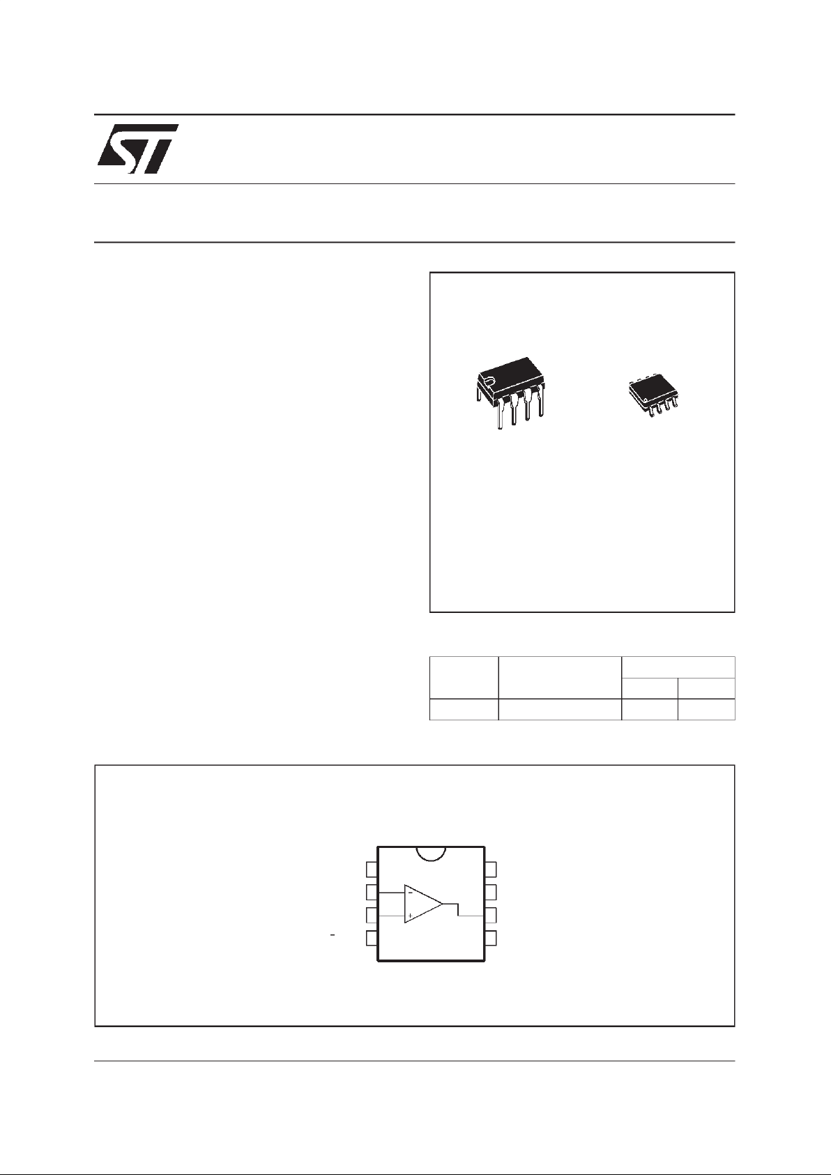
D
SO8
(Plastic Micropackage)
N
DIP8
(Plastic Package)
DESCRIPTION:
The TSH321is a widebandmonolithic operational
amplifier, requiringa minimum close loopgain of 2
for stability.
The TSH321featuresextremelyhigh input impedance (typically greater than 10
12
Ω) allowing direct
interfacingwith high impedance sources.
Low distortion, wide bandwidth and high linearity
make this amplifiersuitableforRF and video applications. Short circuit protection is provided by an
internal current-limiting circuit.
The TSH321 has internal electrostatic discharge
(ESD)protection circuits andfulfillsMILSTD883CClass2.
1/6
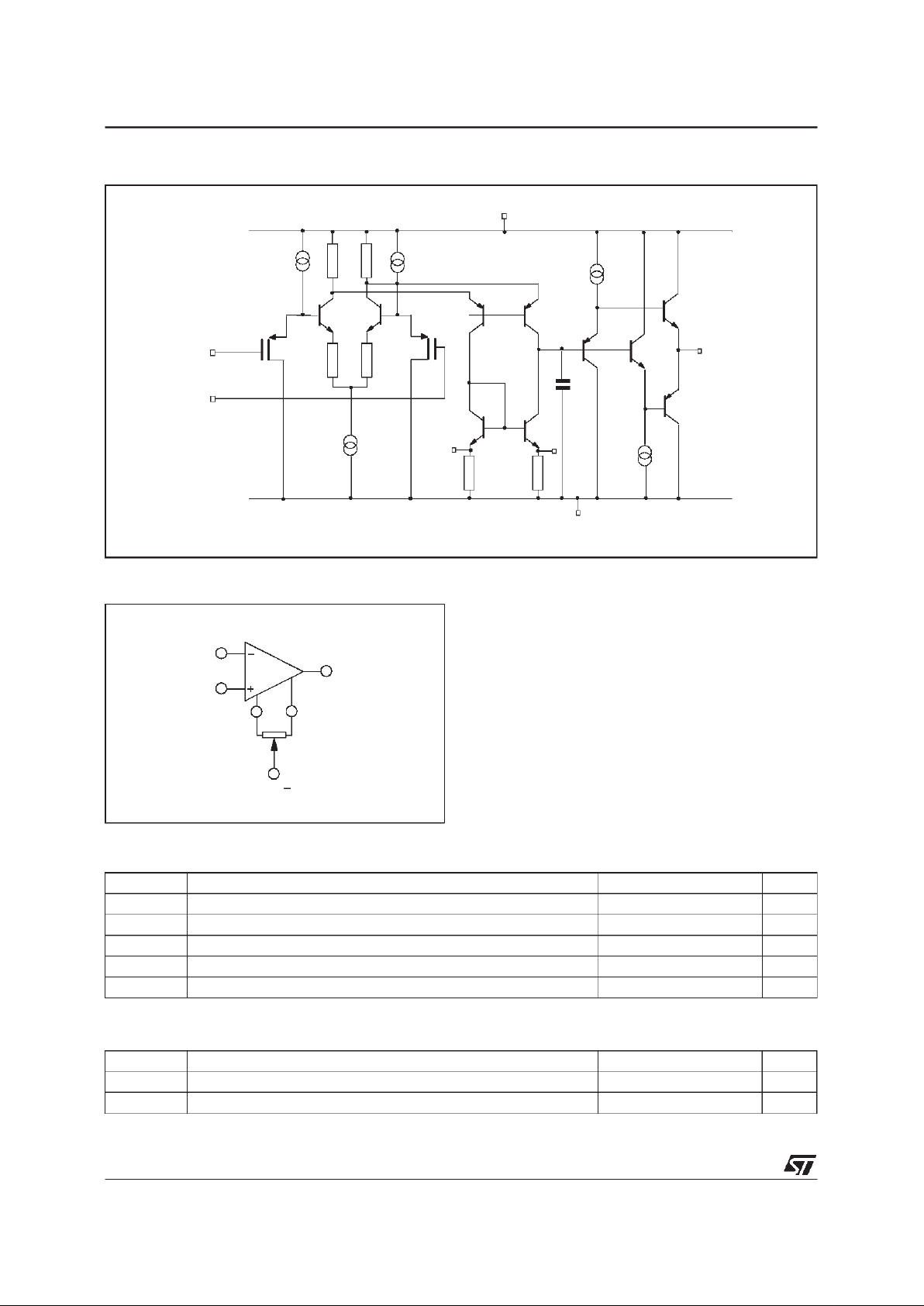
3
non inverting
input
2
inverting
input
1
8
Offset N1
Offset N2
7V
CC
+
C
c
6
output
Internal
V
CC
-
4
V
ref
321-02.EPS
SCHEMATICDIAGRAM
ABSOLUTEMAXIMUMRATINGS
Symbol Parameter Value Unit
V
CC
Supply Voltage ± 7V
V
id
Differential Input Voltage ± 5V
V
i
Input Voltage Range ± 5V
I
in
Current On Offset Null Pins ± 20 mA
T
oper
Operating Free-Air Temperature Range TSH321I -40oC, 125oC
o
C
321-02.TBL
N1
N2
TSH321
100k
Ω
V
CC
321-03.EPS
INPUT OFFSET VOLTAGENULL CIRCUIT
OPERATINGCONDITIONS
Symbol Parameter Value Unit
V
CC
Supply Voltage ± 3to±6V
V
ic
Common Mode Input VoltageRange V
CC
-
to V
CC
+
-3 V
321-03.TBL
TSH321
2/6
 Loading...