

1/5
■ VERY LOW INPUT CURRENT : 2pA typ
■ GAIN BANDWIDTH PRODUCT : 280MHz
■ GAIN OF 2 STABILI TY
■ SLEW RATE : 300V/µs
■ STANDARD PIN OUT
DESCRIPTION
The TSH31 is a low cos t wide bandwidth single
operational amplifier featuring extremely low input
current of 2pA typ.
Other features as high slew rate, fast settling time
and high linearity make it suit able for many ap plications requiring speed and very high input impedance as photo cell amplifier, F et probe, high
speed precision integrator, sample and hold circuit.
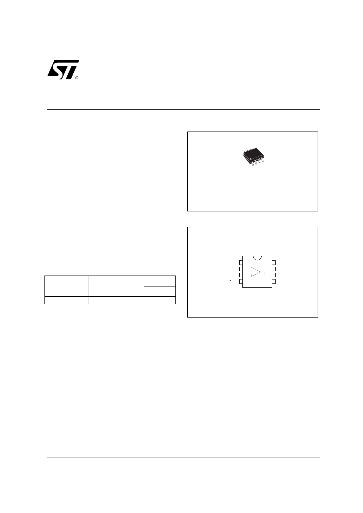
ORDER CODE
D = Small Outline Package (SO) - also available in Tape & Reel (DT)
PIN CONNECTIONS (top view )
Part Number Temperature Range
Package
D
TSH31I -40°C, +125°C
•
D
SO8
(Plastic Micropackage)
1
2
3
4
8
6
5
7
Inverting Input
Non-inverting Input
Output
Offset Null 2
Offset Null 1
N.C.
V
CC
V
CC
+
TSH31
280MHz BANDWIDTH MOS INPUT
SINGLE OPERATIONAL AMPLIFIER
October 2000
TSH31
2/5
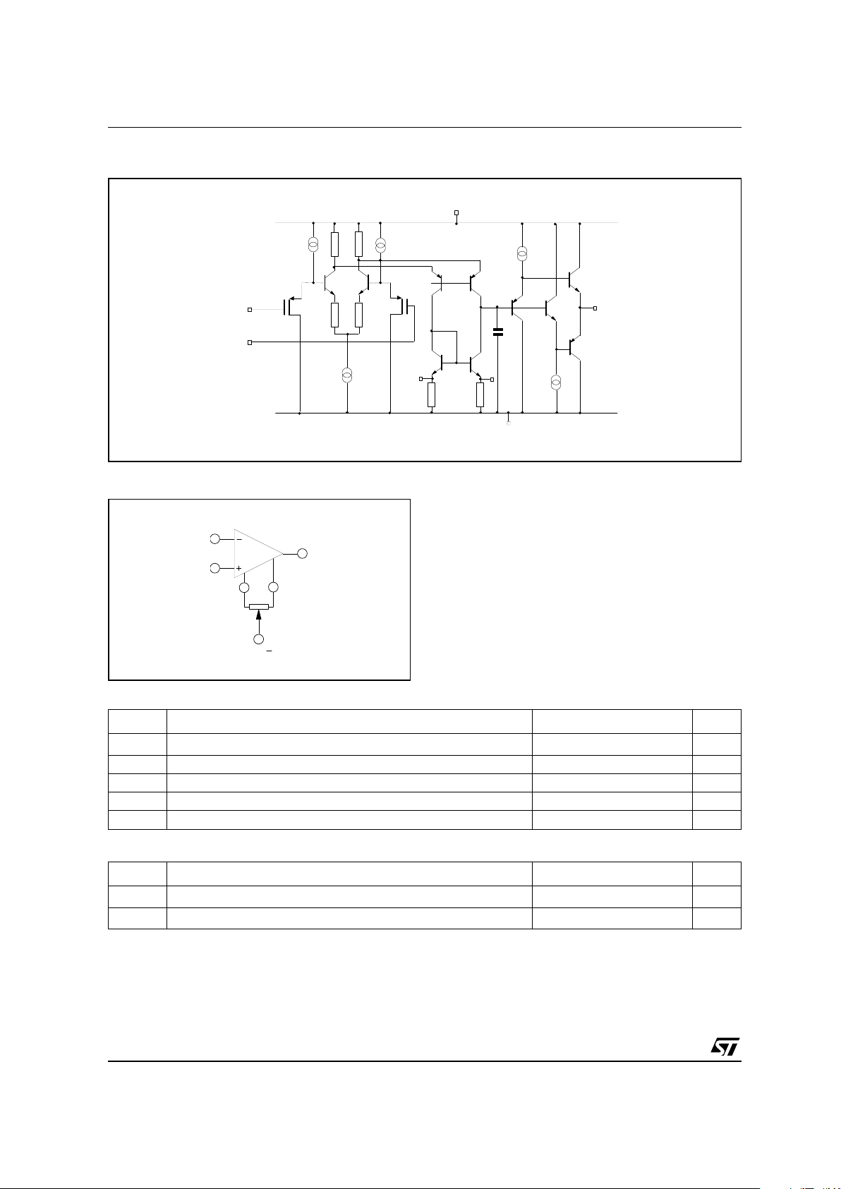
SCHEMATIC DIAGRAM
INPUT OFFSET VOLTAGE NULL CIRCUIT
MAXIMUM RATINGS
OPERATING CONDITIONS
3
non inverting
input
2
inverting
input
1
8
Offset N1
Offset N2
7 V
CC
+
C
c
6
output
Internal
V
CC
-
4
V
ref
N1
N2
TSH31
100k
W
V
CC
Symbol Parameter Value Unit
V
CC
Supply Voltage ±7 V
V
id
Differential Input Voltage ±5 V
V
i
Input Voltage ±5 V
I
in
Current On Offset Null Pins ±20 V
T
oper
Operating Free-Air Temperature range -40 to +125 °C
Symbol Parameter Value Unit
V
CC
Supply Voltage ±3 to ±6 V
V
ic
Common Mode Input Voltage Range
V
CC
-
to V
CC
+
-3
V

TSH31
3/5
ELECTRICAL CHARACTERISTICS
V
CC
= ±5V, T
amb
= 25°C (unless otherwise specified)
Symbol Parameter Min. Typ. Max. Unit
V
io
Input Offset Voltage 3 15 mV
DV
io
Input Offset Voltage Drift
T
min
. ≤ T
amb
≤ T
max.
20
µ
V/°C
I
ib
Input Bias Current
.
2 300 pA
I
io
Input Offset Current
.
2 200 pA
I
CC
Supply Current, no load VCC = ±5V
20 40 mA
Avd
Large Signal Voltage Gain
Vo = ±2.5V R
L
= 100
Ω
200 800
V/V
V
icm
Input Common Mode Voltage Range -5 to +2 -5.5 to +2.5 V
CMR
Common-mode Rejection Ratio
V
ic
= V
icm min.
55 95
dB
SVR
Supply Voltage Rejection Ratio
V
CC
= ±5V to ±3V
45 65
dB
V
o
Output Voltage RL = 100
Ω
±2.5 +3.5
-3.7
V
I
o
Output Short Circuit Current
Vid = ±1V, Vo = 0V ±70
mA
GBP
Gain Bandwidth Product
A
VCL
= 100, RL = 100Ω, f = 7.5MHz
280
MHz
SR
Slew Rate
V
in
= ±2V, A
VCL
= 1, RL = 100
Ω
300
V/µs
e
n
Equivalent Input Voltage Noise f = 1MHz 20 nV/√Hz
φ
m
Phase Margin
A
VM
= 1, RL = 100Ω, CL = 15pF
40 Degrees

TSH31
4/5
EVALUATION CIRCUIT
PRINTED CIRCUIT LAYOUT
As for any high frequency device, a few rules must
be observed when designing the PCB to get the
best performances from this high speed op amp.
From the most to the least important points :
❑ Each power supply lead has to be by-
passed to ground with a 10nF cerami c c apacitor very close to the device and a 10µF
tantalum capacitor.
❑ To provide low inductance and low resist-
ance common return, us e a ground plane
or common point return for power and signal.
❑ All leads must be wide and as short as pos-
sible especially for op amp inputs. This is in
order to decrease parasitic capacitance
and inductance.
❑ Use small resistor values to decrease time
constant with parasitic capacitance.
❑ Choose component sizes as s mall as pos -
sible (SMD).
❑ On output, decrease capacitor load so as
to avoid circuit stability being degraded
which may cause oscillation. You can also
add a serial resistor in order to minimise its
influence.
❑ One can add in paral lel with feedback re-
sistor a few pF ceramic capacitor C
F
adjust-
ed to optimize the settling time.
Input
50
W
1k
W
10nF
10
m
F
C
F
-5V
+5V
10nF
Outpu
t
50
W
10mF
1k
W

TSH31
5/5
Inform ation fu rnished is beli eved to b e accur ate an d reliab le. Howe ver, ST Micro electron ics ass umes no respo nsibility for th e
consequences of use of such information nor f or any infringement of patent s or other ri ghts of t hird parti es which ma y result
from its use. No license is granted by implication or otherwise under any patent or patent rights of STMicroelectronics.
Specifications mentioned in this publication are subject to cha nge witho ut notice. This publication sup erse des and rep laces all
information previously supplied. STMicroelectroni cs products are not authorized for use as critical components in life support
devices or systems without express written approval of STMicroelectronics.
© The ST logo is a registered trademark of STMicroelectronics
© 2000 STM icroelectronics - Printed in Italy - All Rights Reserv ed
STMicroelectronics GROUP OF COMPANIES
Austra lia - Brazil - Chi na - Finland - F rance - Germ any - Hong Ko ng - India - Italy - Japan - Mal aysia - Malt a - M orocco
Singap ore - Spain - Sweden - Switzerland - U ni ted Kingdom
© htt p://w ww.st.com
PACKAGE MECHANICAL DATA
8 PINS - PLASTIC MICROPACKAGE (SO)
Dim.
Millimeters Inches
Min. Typ. Max. Min. Typ. Max.
A 1.75 0.069
a1 0.1 0.25 0.004 0.010
a2 1.65 0.065
a3 0.65 0.85 0.026 0.033
b 0.35 0.48 0.014 0.019
b1 0.19 0.25 0.007 0.010
C 0.25 0.5 0.010 0.020
c1 45° (typ.)
D 4.8 5.0 0.189 0.197
E 5.8 6.2 0.228 0.244
e 1.27 0.050
e3 3.81 0.150
F 3.8 4.0 0.150 0.157
L 0.4 1.27 0.016 0.050
M 0.6 0.024
S 8° (max.)
 Loading...