

TSH151
WIDE BANDWIDTHAND MOS INPUTS
SINGLE OPERATIONALAMPLIFIER
June 1998
ORDERCODES
Part
Number
Temperature
Range
Package
ND
TSH151C 0
o
C, 70oC ••
TSH151I -40
o
C, 125oC ••
151-01.TBL
1
2
3
4
8
6
5
7
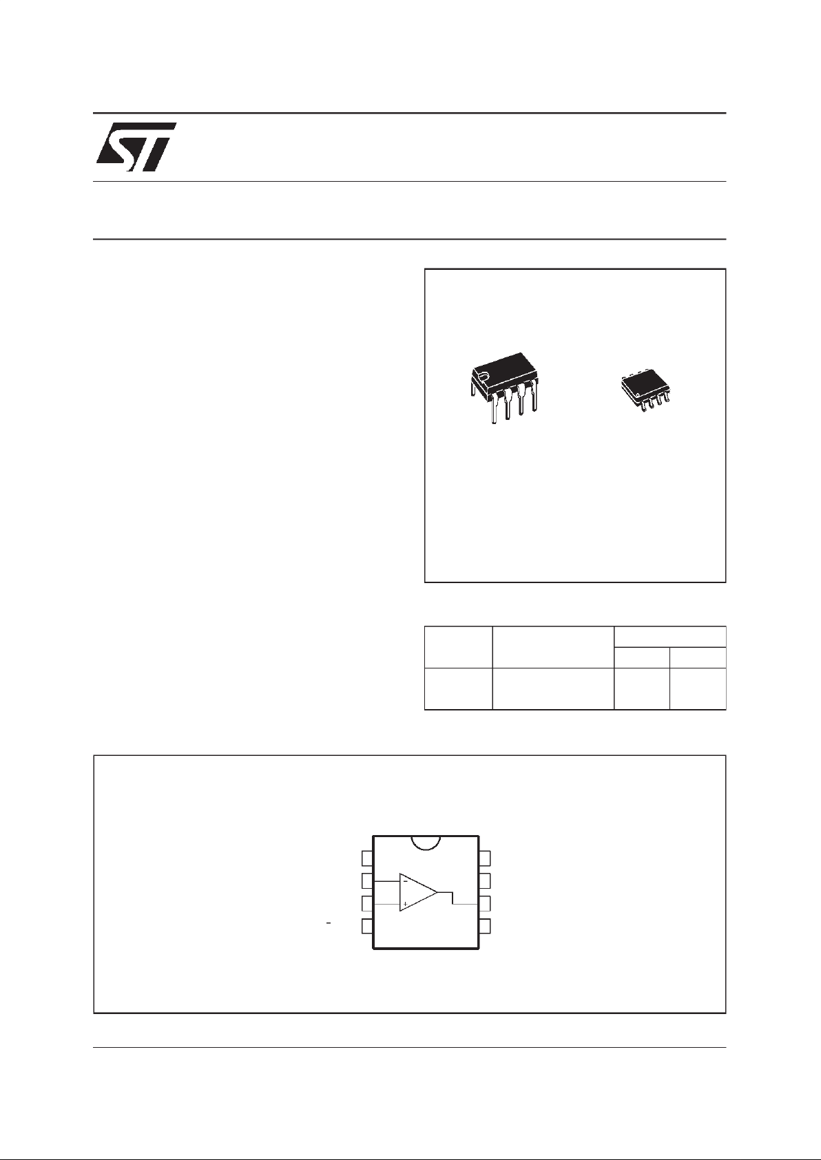
Inverting Input
Non-invertingInput
Output
Offset Null 2Offset Null 1
N.C.
V
CC
V
CC
+
151-01.EPS
PINCONNECTIONS (top view)
.LOW DISTORTION
.GAIN BANDWIDTH PRODUCT : 150MHz
.UNITY GAIN STABLE
.SLEW RATE : 200V/µs
.VERY FASTSETTLING TIME : 70ns (0.1%)
.VERY HIGH INPUT IMPEDANCE
D
SO8
(Plastic Micropackage)
N
DIP8
(Plastic Package)
DESCRIPTION:
The TSH151is a widebandmonolithic operational
amplifier,internallycompensatedforunity-gainstability.
The TSH151features extremely high input impedance (typically greater than 10
12
Ω) allowing direct
interfacingwith high impedance sources.
Low distortion, wide bandwidth and high linearity
make this amplifiersuitableforRF and video applications. Short circuit protection is provided by an
internal current-limiting circuit.
The TSH151 has internal electrostatic discharge
(ESD)protection circuits andfulfillsMILSTD883CClass2.
1/7
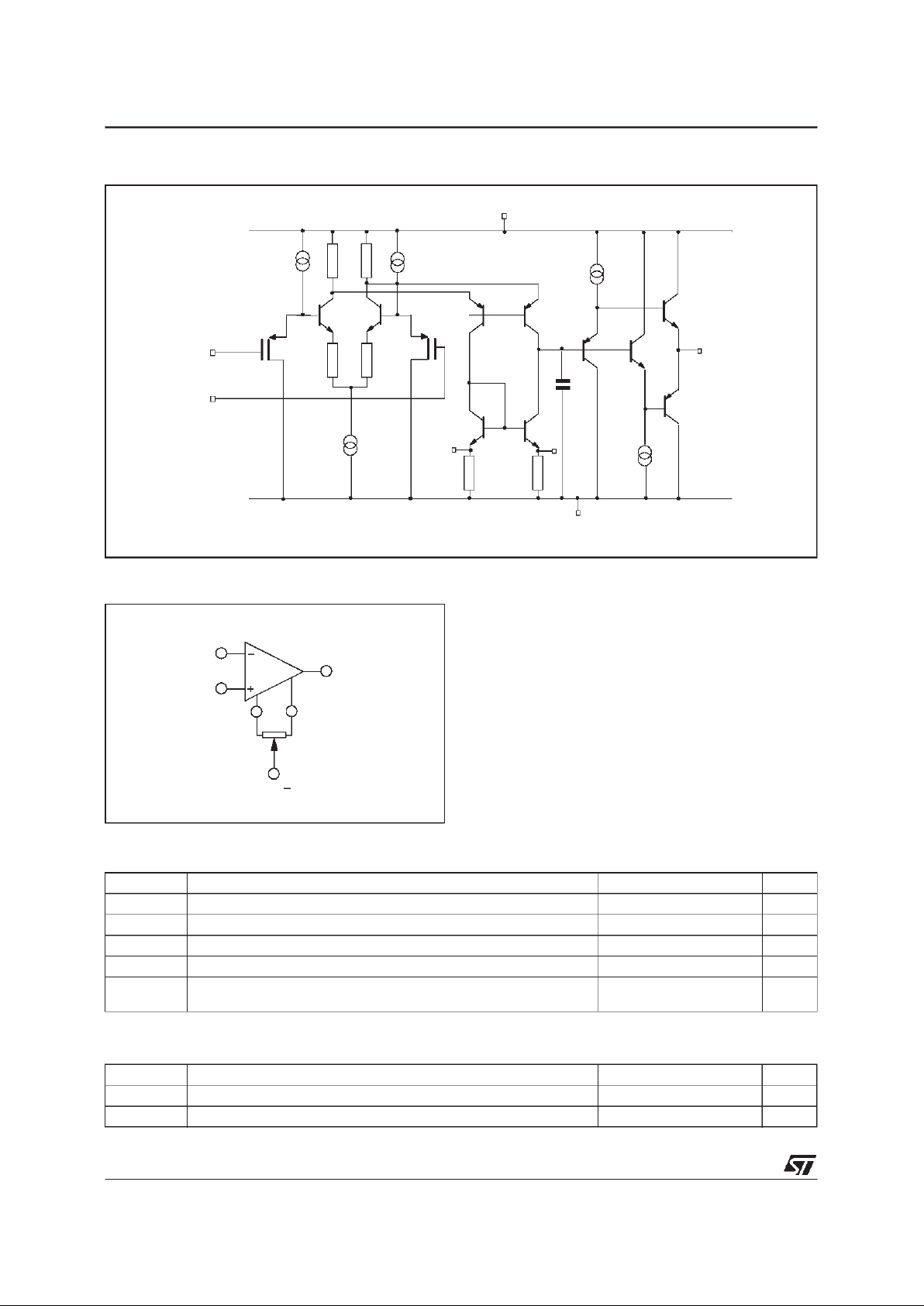
3
non inverting
input
2
inverting
input
1
8
Offset N1
Offset N2
7V
CC
+
C
c
6
output
Internal
V
CC
-
4
V
ref
151-02.EPS
SCHEMATICDIAGRAM
ABSOLUTEMAXIMUMRATINGS
Symbol Parameter Value Unit
V
CC
Supply Voltage ±7V
V
id
Differential Input Voltage ±5V
V
i
Input Voltage Range ±5V
I
in
Current On Offset Null Pins ±20 mA
T
oper
Operating Free-Air Temperature Range TSH151C
TSH151I
0oC, 70oC
-40
o
C, 15oC
o
C
151-02.TBL
N1
N2
TSH151
100k
Ω
V
CC
151-03.EPS
INPUT OFFSET VOLTAGENULL CIRCUIT
OPERATINGCONDITIONS
Symbol Parameter Value Unit
V
CC
Supply Voltage ±3to±6V
V
ic
Common Mode Input VoltageRange V
CC
-
to V
CC
+
-3 V
151-03.TBL
TSH151
2/7

ELECTRICALCHARACTERISTICS
V
CC
= ± 5V, T
amb
=25oC (unlessotherwisespecified)
Symbol Parameter
TSH151C, I
Unit
Min. Typ. Max.
V
io
Input Offset Voltage
T
min
≤ T
amb
≤ T
max.
0.5 10
12
mV
DV
io
Input Offset Voltage Drift
T
min
≤ T
amb
≤ T
max.
10
µV/
o
C
I
ib
Input Bias Current 2 300 pA
I
io
Input Offset Current 2 200 pA
I
CC
Supply Current, no load
V
CC
= ± 5V
V
CC
= ± 3V
V
CC
= ±6V
T
min
≤ T
amb
≤ T
max.
VCC= ± 5V
23
21
25
30
28
40
32
mA
A
vd
Large Signal VoltageGain
V
o
= ±2.5V
R
L
= ∞
R
L
= 100Ω
R
L
=50Ω
800
300
200
1300
850
650
V/V
V
icm
Input Common Mode Voltage Range -5 to +2 -5.5 to +2.5 V
CMR Common Mode Rejection Ratio V
ic=Vicm min.
60 100 dB
SVR Supply VoltageRejection Ratio
V
CC
= ± 5V to ± 3V 50 70
dB
V
o
Output Voltage RL= 100Ω
R
L
=50Ω
T
min
≤ T
amb
≤ T
max.
RL= 100Ω
R
L
=50Ω
±3
±2.8
± 2.9
± 2.7
+3.5
-3.7
+3.3
-3.5
V
I
o
Output Short Circuit Current
V
id
= ±1V, Vo=0V ±50 ±100
mA
GBP Gain Bandwidth Product
A
VCL
= 100, RL= 100Ω,CL= 15pF,f = 7.5MHz 150
MHz
SR Slew Rate
V
in
= ± 2V,A
VCL
=1,RL= 100Ω,CL= 15pF 100 200
V/µs
e
n
Equivalent Input VoltageNoise
R
S
=50Ω
fo = 1kHz
fo = 10kHz
fo = 100kHz
fo = 1MHz
20
18.2
18.1
18.2
nV
√Hz
K
ov
Overshoot
V
in
= ± 2V,A
VCL
=1,RL= 100Ω,CL= 15pF 10
%
t
s
Settling Time 0.1% - (note1)
V
in
= ± 1V,A
VCL
=-1 70
ns
t
r,tf
Rise and Fall Time - (note1)
V
in
= ±100mV,A
VCL
=2 5
ns
t
d
Delay Time - (note 1)
V
in
= ±100mV,A
VCL
=2 4
ns
∅m Phase Margin
A
VM
=1,RL= 100Ω, CL= 15pF 45
Degrees
THD Total Harmonic Distortion
A
VCL
= 10, f = 1KHz, Vo= ± 2.5V,no load 0.02
%
FPB Full Power Bandwidth - (note 2)
V
o
= 5Vpp, RL= 100Ω
V
o
= 2Vpp, RL= 100Ω
13
32
MHz
Note 1 : See test waveform figure
Note 2 : Full powerbandwidth =
SR
Π V
opp
151-04.TBL
TSH151
3/7

V
in
50%
t
d
t
r
90%
t
s
0.1% of edge amplitude
10%
151-04.EPS
TEST WAVEFORM
Input
50Ω
1kΩ
1kΩ
10nF
10µF
C
F
-5V
+5V
10nF
10µF
50
Ω
Output
151-05.EPS
EVALUATION CIRCUIT
As for any high frequencydevice, a fewrules must
be observedwhendesigningthe PCBto getthe best
performancesfrom your this speed op amp.
From the most to the least important points :
• Each power supply lead has to be bypassed
to ground with a 10nF ceramic capacitor very
close to the deviceand a 10µF tantalum ca-
pacitor.
• To providelow inductanceand low resistance
common return, use a ground plane or common point return for power and signal.
• All leads must be wideand as short as possi-
ble especially for op amp inputs. This is in
order to decrease parasitic capacitance and
inductance.
• Use small resistor values to decrease time
constantwith parasitic capacitance.
• Choosecomponentsizesassmallaspossible
(SMD).
• On output, decrease capacitor load so as to
avoid circuit stability being degraded which
may cause oscillation. One can also add a
serial resistor in order to minimise its influence.
• One can addin parallelwithfeedbackresistor
a few pF ceramic capacitor C
F
adjusted to
optimizethe settlingtime.
PRINTEDCIRCUIT LAYOUT
TSH151
4/7

.LOW DISTORTION
.GAIN BANDWIDTH PRODUCT : 150MHz
.UNITY GAIN STABLE
.SLEW RATE : 200V/µs
.VERY FASTSETTLING TIME : 70ns (0.1%)
.VERY HIGH INPUT IMPEDANCE
MACROMODEL
** Standard Linear Ics Macromodels, 1993.
** CONNECTIONS :
* 1 INVERTING INPUT
* 2 NON-INVERTING INPUT
* 3 OUTPUT
* 4 POSITIVEPOWER SUPPLY
* 5 NEGATIVEPOWER SUPPLY
.SUBCKT TSH151 1 3 2 4 5 (analog)
**********************************************************
.MODEL MDTH D IS=1E-8 KF=3.322525E-14 CJO=10F
* INPUT STAGE
RESD1 2 202 150
RESD2 1 201 150
CIP 202 5 10.000000E-12
CIN 201 5 10.000000E-12
EIP 10 5 202 5 1
EIN 16 5 201 5 1
RIP 10 11 2.600000E-01
RIN 15 16 2.600000E-01
RIS 11 15 1.683423E-01
DIP 11 12 MDTH 400E-12
DIN 15 14 MDTH 400E-12
VOFP 12 13 DC 0.000000E+00
VOFN 13 14 DC 0
IPOL 13 5 1.000000E-03
CPS 11 15 8E-09
DINN 17 13 MDTH 400E-12
VIN 17 5 1.500000e+00
DINR 15 18 MDTH 400E-12
VIP 4 18 5.000000E-01
FCP 4 5 VOFP 2.200000E+01
FCN 5 4 VOFN 2.200000E+01
* AMPLIFYING STAGE
FIP 5 19 VOFP 3.800000E+02
FIN 5 19 VOFN 3.800000E+02
RG1 19 5 1.455096E+03
RG2 19 4 1.455096E+03
CC 19 29 2.000000E-09
HZTP 29 30 VOFP 100
HZTN 30 5 VOFN 100
DOPM 19 22 MDTH 400E-12
DONM 21 19 MDTH 400E-12
HOPM 22 28 VOUT 5.000000E+02
VIPM 28 4 5.000000E+01
HONM 21 27 VOUT 5.000000E+02
VINM 5 27 5.000000E+01
EOUT 26 23 19 5 1
VOUT 23 5 0
ROUT 26 3 9.978126E+00
COUT 3 5 1.000000E-13
DOP 19 25 MDTH 400E-12
VOP 4 25 1.946965E+00
DON 24 19 MDTH 400E-12
VON 24 5 1.946965E+00
.ENDS
Applies to : TSH151C,I
ELECTRICAL CHARACTERISTICS
V
CC
=±5V, T
amb
=25oC (unlessotherwise specified)
Symbol Conditions Value Unit
V
io
0mV
A
vd
RL= 100Ω 1.18 V/mV
I
CC
No load, per operator 23 mA
V
icm
-5 to 2.5 V
V
OH
RL= 100Ω +3.6 V
V
OL
RL= 100Ω -3.6 V
I
sink
VO= 0V 108 mA
I
source
VO= 0V 108 mA
GBP R
L
= 100
Ω,
CL= 15pF 130 MHz
SR R
L
= 100
Ω,
CL= 15pF 172 V/µs
∅mR
L
= 100
Ω,
CL= 15pF 25 Degrees
t
s
AV= -1 at 0.1% 40 ns
TSH151
5/7

PM-DIP8.EPS
PACKAGEMECHANICAL DATA
8 PINS - PLASTICDIP
Dimensions
Millimeters Inches
Min. Typ. Max. Min. Typ. Max.
A 3.32 0.131
a1 0.51 0.020
B 1.15 1.65 0.045 0.065
b 0.356 0.55 0.014 0.022
b1 0.204 0.304 0.008 0.012
D 10.92 0.430
E 7.95 9.75 0.313 0.384
e 2.54 0.100
e3 7.62 0.300
e4 7.62 0.300
F 6.6 0260
i 5.08 0.200
L 3.18 3.81 0.125 0.150
Z 1.52 0.060
DIP8.TBL
TSH151
6/7

PM-SO8.EPS
PACKAGEMECHANICAL DATA
8 PINS - PLASTICMICROPACKAGE(SO)
Dimensions
Millimeters Inches
Min. Typ. Max. Min. Typ. Max.
A 1.75 0.069
a1 0.1 0.25 0.004 0.010
a2 1.65 0.065
a3 0.65 0.85 0.026 0.033
b 0.35 0.48 0.014 0.019
b1 0.19 0.25 0.007 0.010
C 0.25 0.5 0.010 0.020
c1 45
o
(typ.)
D 4.8 5.0 0.189 0.197
E 5.8 6.2 0.228 0.244
e 1.27 0.050
e3 3.81 0.150
F 3.8 4.0 0.150 0.157
L 0.4 1.27 0.016 0.050
M 0.6 0.024
S8
o
(max.)
SO8.TBL
Information furnished is believed to be accurate and reliable. However, STMicroelectronics assumes no responsibility for the
consequences of use of such information nor for any infringement of patents or other rights of third parties which may result from
its use. No license is granted by implication or otherwise under any patent or patent rights of STMicroelectronics. Specifications
mentioned in this publication are subject to change without notice. This publication supersedes and replaces all information
previously supplied.STMicroelectronics productsare notauthorized foruseas criticalcomponents inlife supportdevices or systems
without express written approval of STMicroelectronics.
The ST logo is a trademark of STMicroelectronics
1998 STMicroelectronics – Printed in Italy – All Rights Reserved
STMicroelectronics GROUP OF COMPANIES
Australia- Brazil - Canada - China - France - Germany - Italy - Japan - Korea - Malaysia - Malta - Mexico - Morocco
The Netherlands - Singapore - Spain- Sweden - Switzerland - Taiwan- Thailand - United Kingdom - U.S.A.
ORDERCODE :
TSH151
7/7
 Loading...