

Datasheet TSA1005-40IF, TSA1005-20IFT, TSA1005-20IF, TSA1005, TSA1005-40IFT Datasheet (SGS Thomson Microelectronics)
1/22
■ 10-bit, dual-channel A/D converter in deep
submicron CMOS technology, 20/40Msps
■ Single supply voltage: 2.5V
Independent supply for CMOS output stage
with 2.5V/3.3V capability
■ ENOB=9.5 @ 20Msps, ENOB=9.2 @
40Msps, Fin=10MHz
■ SFDR typically up to 62.5dB @ 40Msps,
Fin=10MHz.
■ 1GHz analog bandwidth Track-and-Hold
■ Common clocking between channel s
■ Multiplexed outputs
DESCRIPTION
The TSA1005 belongs to a new generation of high
speed, dual-channel Anal og to Digital conv erters,
processed in a mainstream 0.25 µm CMOS technology and yielding high performances.
The TSA1005 is specifically designed for applications requiring a very low noise floor, high SFDR
and good isolation b etween channels. It is bas ed
on a pipeline structure and digital error correction,
providing high static linearity at 20/40 Msp, and
Fin = 10 MHz.
For each channel, a voltage reference is integrated to simplify the design and minimize external
components. It is nevertheless possible to use the
circuit with external references.
Each ADC output is multiplexed on a common bus
with small number of pins. A tri-state capability is
available for the output signals, a llowing for chip
selection. The input signals of the ADC mus t be
differentially driven.
The TSA1005 is supports an extended (0 to
+85°C) temperature range , and is available in the
small 48-pin TQFP package.
APPLICATIONS
■ Medical imaging and ultrasound
■ I/Q signal processing applications
■ High speed data acquisition system
■ Portable instrumentation
■ High resolution fax and scanners
ORDER CODE
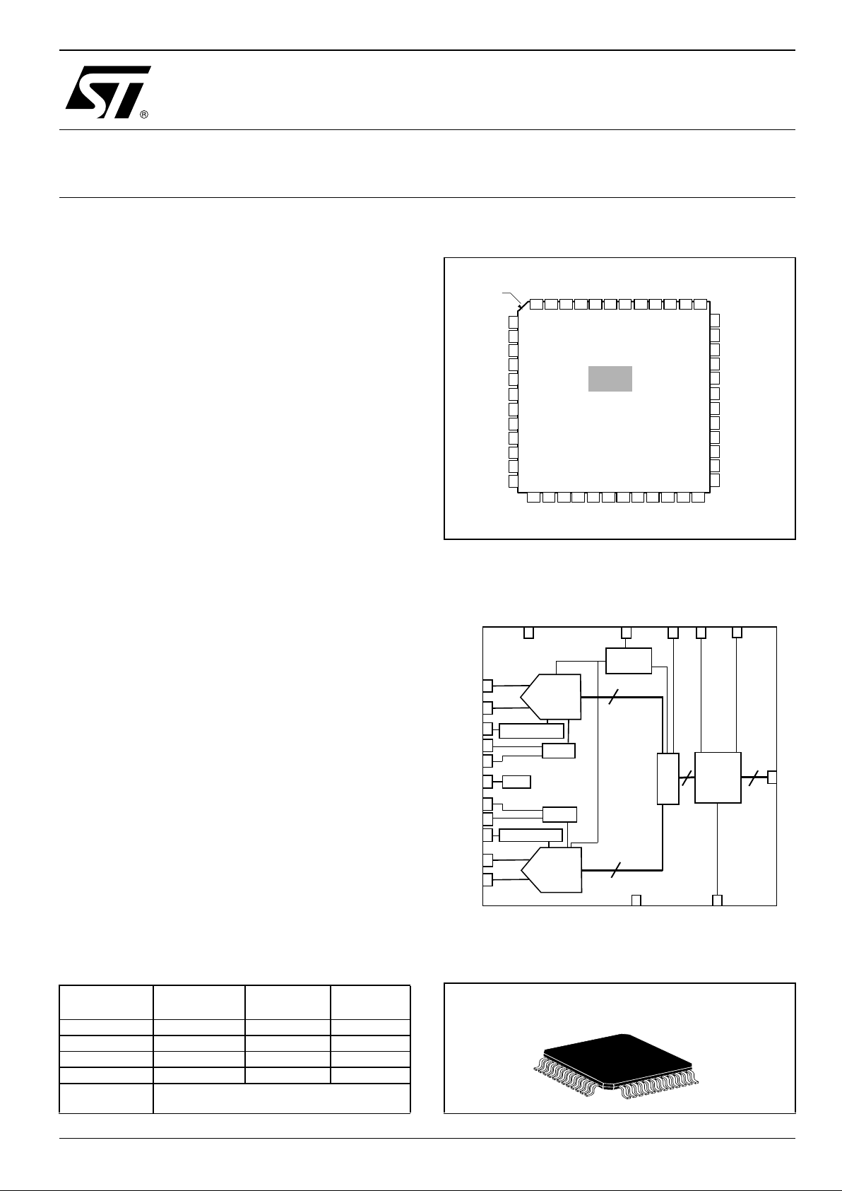
PIN CONNECTIONS (top view)
BLOCK DIAGRAM
PACKAGE
Part Number
Temperature
Range
Status Conditioning
TSA100 5-20IF -40°C to +85°C Sample Tr ay
TSA1005-20IFT -40°C to +85°C Sample Tape & Reel
TSA1005I-40IF 0°C to +85°C Production Tray
TSA1005-40IFT 0°C to +85°C Production T ape & Reel
EVAL1005-20/BA
EVAL1005-40/BA
Evaluation board
D3
D4
D5
D6
D7
D8
D9(MSB)
AVCCB
index
corner
1
2
3
4
5
6
7
8
9
10
11
32
31
30
29
28
27
26
13 14 15 16 17 18 19 20 21 22
47
25
33
12
23 24
35
34
36
48 44 43 42 41 40 39 38
37
46 45
TSA1005
VCCBE
GNDBE
AGND
INI
AGND
AGND
IPOL
AGND
AGND
INBQ
INIB
AGND
INQ
D0(LSB)
D1
REFMI
NC
OEB
AVCC
REFPI
INCMI
AVCC
VCCBI
GNDBE
VCCBI
NC
VCCBE
SELECT
CLK
DGND
REFPQ
AGND
AVCC
DGND
DVCC
DVCC
INCMQ
REFMQ
GNDBI
D2
Timing
Buffers
IPOL
CLK
+2.5V/3.3V
VINI
VINBI
OEB
VINCMI
GND
VINQ
VINBQ
VINCMQ
AD 10
I channel
AD 10
Q channel
10
10
10
10
M
U
X
REF I
REF Q
SELECT
VREFPI
VREF PQ
Polar.
VREFMI
VREFM Q
common mod e
common mode
D0
TO
D9
GNDBE
VCCBE
7 × 7 mm TQFP48
TSA1005
DUAL-CHANNEL, 10-BIT, 20/40MSPS A/D CONVERTER
June 2003
TSA1005
2/22
ABSOLUTE MAXIMUM RATINGS
OPERATING CONDITIONS
Symbol Parameter Values Unit
AVCC
Analog Supply voltage
(1)
0 to 3.3 V
DVCC
Digital Supply voltage
1)
0 to 3.3 V
VCCBE
Digital buffer Supply voltage
1)
0 to 3.6 V
VCCBI
Digital buffer Supply voltage
1)
0 to 3.3 V
IDout Digital output current -100 to 100 mA
Tstg Storage temperature +150 °C
ESD
HBM: Human Body Model
(2)
CDM: Charged Device Model
(3)
2
1.5
kV
Latch-up
Class
(4)
A
1 All voltage values, except for differential voltage, are with respect to the network ground terminal. The magnitude of input and output volt-
ages must not excee d -0.3 V or VCC
2 ElectroStatic Discharge pulse (ESD pulse) simulating a human body discharge of 100 pF through 1.5 k
Ω
3 Discha rge to Ground of a device that has been prev i ously charged.
4 Corpor ate ST Microel ectronics procedure nu mber 001869 5
Symbol Parameter
TSA1005-20
(1)
TSA1005-40
Min. Typ. Max. Min. Typ. Max. Unit
AVCC Analog Supply voltage 2.25 2.5 2.7 2.25 2.5 2.7 V
DVCC Digital Supply voltage 2.25 2.5 2.7 2.25 2.5 2.7 V
VCCBE External Digital buffer Supply voltage 2.25 2.5 3.5 2.25 2.5 3.5 V
VCCBI Internal Digital buffer Supply voltage 2.25 2.5 2.7 2.25 2.5 2.7 V
VREFPI
VREFPQ
Forced top voltage reference 0.94 1.4 0.94 1.4 V
VREFMI
VREFMQ
Forced bottom reference voltage 0 0.4 0 0.4 V
INCMI
INCMQ
Forced input common mode voltage 0.2 1 0.2 1 V
TSA1005
3/22
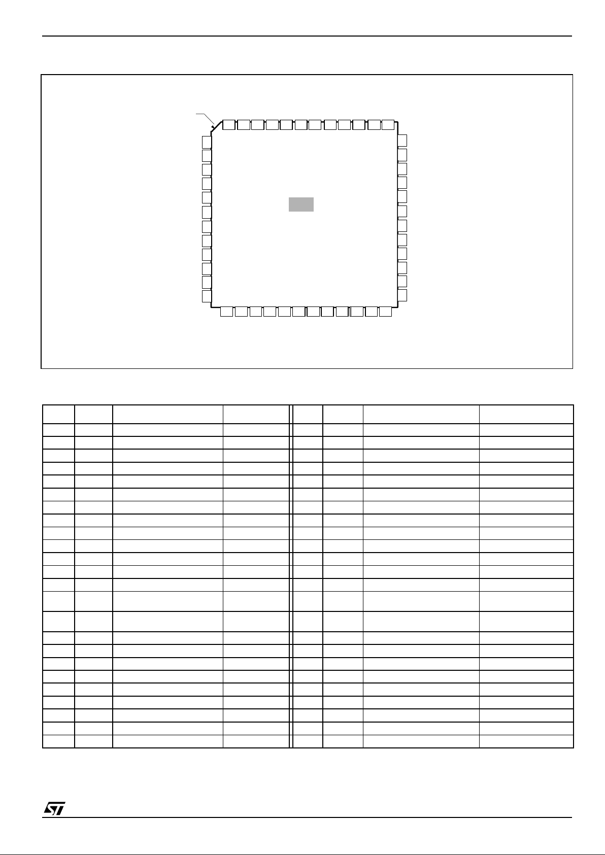
PIN CONNECTIONS (top view)
PIN DESCRIPTION
D3
D4
D5
D6
D7
D8
D9(MSB)
AVCCB
index
corner
1
2
3
4
5
6
7
8
9
10
11
32
31
30
29
28
27
26
13 14 15 16 17 18 19 20 21 22
47
25
33
12
23 24
35
34
36
48 44 43 42 41 40 39 38
37
46 45
TSA1005
VCCBE
GNDBE
AGND
INI
AGND
AGND
IPOL
AGND
AGND
INBQ
INIB
AGND
INQ
D0(LSB)
D1
REFMI
NC
OEB
AVCC
REFPI
INCMI
AVCC
VCCBI
GNDBE
VCCBI
NC
VCCBE
SELECT
CLK
DGND
REFPQ
AGND
AVCC
DGND
DVCC
DVCC
INCMQ
REFMQ
GNDBI
D2
Pin No Name Description Observation Pin No Name Description Observation
1 AGND Analog gro und 0V 25 GNDBE Digital buffer ground 0V
2 INI I channel analog input 26 VCCBE Digital Buffer power supply 2.5V/3.3V
3 AGND Analog ground 0V 27 D9(MSB) Most Significant Bit output CMOS output (2.5V/3.3V)
4 INBI I channel inverted analog input 28 D8 Digital output CMOS output (2.5V/3.3V)
5 AGND Analog ground 0V 29 D7 Digital output CMOS output (2.5V/3.3V)
6 IPOL Ana l og bias current input 30 D6 Digital output CMOS output (2.5V/3 .3V)
7 AVCC Analog power s upply 2.5V 31 D5 Digital output CMOS outp ut (2.5 V/3.3V)
8 AGND Analog ground 0V 32 D4 Digital output CMOS output (2.5V/3.3V)
9 INQ Q channel analog input 33 D3 Digital output CMOS output (2.5V/3.3V)
10 AGND Analog ground 0V 34 D2 Digital output CMOS output (2.5V/3.3V)
11 INBQ Q channel inverted analog input 35 D1 Digital output CMOS output (2.5V/3.3V)
12 AGND Analog ground 0V 36 D0(LSB) Least Significant Bit output CMOS output (2.5V/3.3V)
13 REFPQ Q channel top reference voltage 37 NC Non connected
14 REFMQ Q channel bottom reference
voltage
0V 38 NC Non connected
15 INCMQ Q channel input common mode 39 VCCBE Digital Buffer power supply 2.5V/3.3V - See Application
Note
16 AGND Analog ground 0V 40 GNDBE Digital buffer ground 0V
17 AVCC Analog power supply 2.5V 41 VCCBI Digital Buffer power supply 2.5V
18 DVCC Digital power supply 2.5V 42 VCCBI Digital Power Supply 2.5V
19 DGND Digita l ground 0V 43 OEB Output Enable input 2.5V/3.3V CMOS input
20 CLK Clock input 2.5V CMOS input 44 AVCC Analog power supply 2.5V
21 SELECT Channel selection 2.5V CMOS input 45 AVCC Analog power supply 2.5V
22 DGND Digita l ground 0V 46 INCM I I channel input common mode
23 DVCC Digital power sup ply 2.5V 47 REFMI I channel bottom ref erenc e voltage 0V
24 GNDBI Digital buffer ground 0V 48 REFPI I chan nel top refer ence voltage
TSA1005
4/22
ELECTRICAL CHARACTERISTICS
AVCC = DVCC = VCCB = 2.5 V, Fs = 20/40 Msps, Fin = 10.13 MHz, Vin@ -1 dBFS, VREFP = 0.8 V,
VREFM = 0 V
Tamb = 25°C (unless otherwise specified)
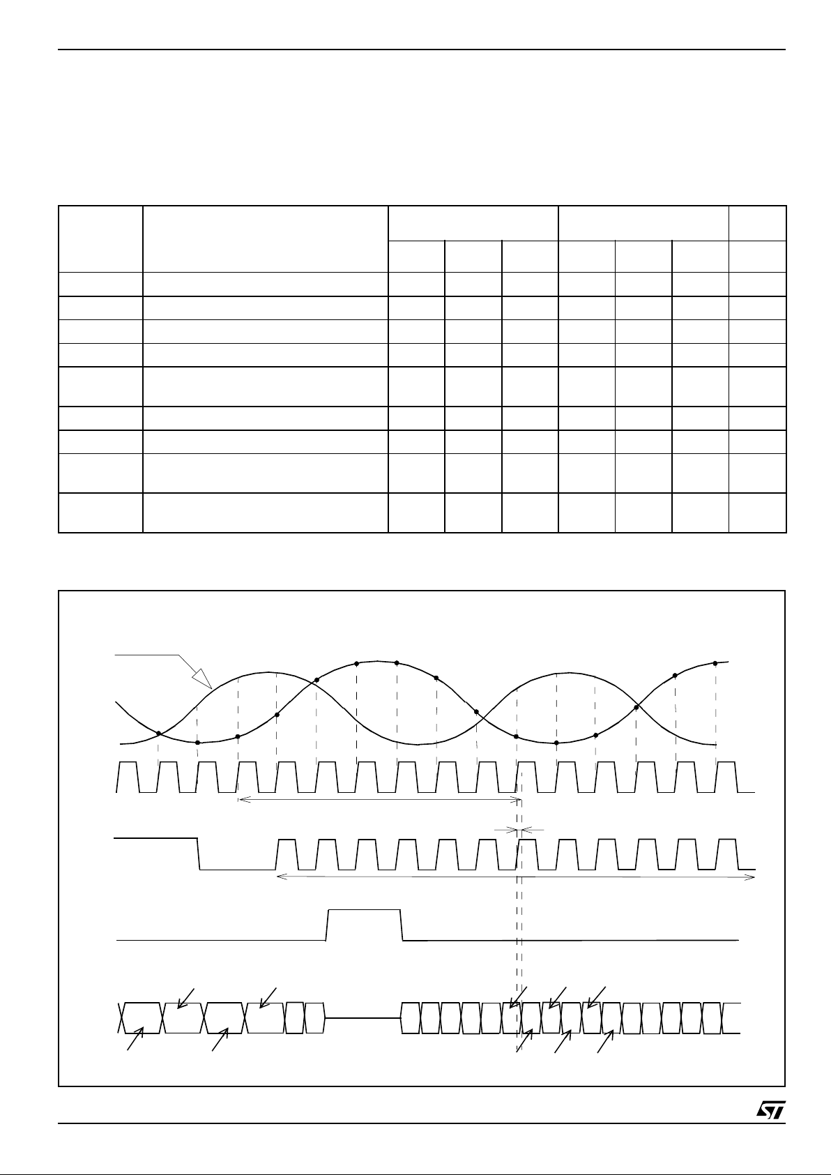
TIMING CHARACTERISTICS
TIMING DIAGRAM
Symbol Parameter.
TSA1005-20
(1)
1 P reliminary data.
TSA1005-40
Min. Typ. Max. Min. Typ. Max. Unit
FS Sampling Frequency 0.5 20 0.5 40 MHz
DC Clock Duty Cycle 50 45 50 55 %
TC1 Clock pulse width (high) 25 12.5 ns
TC2 Clock pulse width (low) 25 12.5 ns
Tod
Data Output Delay (Clock edge to Data
Valid) - 10pF load capacitance
55ns
Tpd I Data Pipeline delay for I channel 7 7 cycles
Tpd Q Data Pipeline delay for Q channel 7.5 7.5 cycles
Ton
Falling edge of OEB to digital output
valid data
11ns
Toff
Rising edge of OEB to digital output
tri-state
11ns
N-1
N
N+1
N+6
N+7
N+2
N+5
N+3
N+4
N+8
CLK
Tpd I + Tod
N+9
N+10
N+11
N+12
N+13
DATA
OUTPUT
sample N+1
I channel
sample N
Q channel
sample N+1
Q channel
sample N+2
I channel
sample N+2
Q channel
sample N+3
I channel
OEB
Simultaneous sampling
on I/Q channels
SELECT
sample N-9
I channel
sample N-8
I channel
samp le N-7
Q channel
sample N-6
Q channel
CLOCK AND SELECT CONNECTED TOGETHER
Tod
I
Q
TSA1005
5/22
CONDITIONS
A VCC = DVCC = VCCB = 2.5V , Fs= 20/40Msps, Fin=2MHz, Vin@ -1dBFS, VREFM=0V
Tamb = 25°C (unless otherwise specified)
ANALOG INPUTS
DIGITAL INPUTS AND OUTPUTS
REFERENCE VOLTAGE
Symbol Parameter
TSA1005-20
(1)
TSA1005-40
Min. Typ. Max. Min. Typ. Max. Unit
VIN-VINB Full scale reference voltage 1.1 2.0 2.8 1.1 2.0 2.8 Vpp
Cin Input capacitance 7.0 7 pF
Req Equivalent input resistor 3.3 1.6 K
Ω
BW
Analog Input Bandwidth
Vin Full scale, Fs max
1000 1000 MHz
ERB Effective Resolution Bandwidth 70 70 MHz
1 P reliminary data
Symbol Parameter Test conditions Min Typ Max Unit
Clock and Select inputs
VIL Logic "0" voltage 0 0.8 V
VIH Logic "1" voltage 2.0 2.5 V
OEB input
VIL Logic "0" voltage 0
0.25 x
VCCBE
V
VIH Logic "1" voltage
0.75 x
VCCBE
VCCBE V
Digital Outputs
VOL
Logic "0" voltage
Iol=10µA
0
0.1 x
VCCBE
V
VOH
Logic "1" voltage
Ioh=10µA 0.9 x
VCCBE
VCCBE V
IOZ High Impedance leakage current OEB set to VIH -1.67 0 1.67 µA
C
L
Output Load Capacitance 15 pF
Symbol Parameter
TSA1005-20
(1)
TSA1005-40
Min. Typ. Max. Min. Typ. Max. Unit
VREFPI
VREFPQ
Top internal reference voltage 0.81 0.88 0.94 0.81 0.88 0.94 V
VINCMI
VINCMQ
Input common mode voltage 0.41 0.46 0.50 0.41 0.46 0.50 V
TSA1005
6/22
CONDITIONS
AVCC = DVCC = VCCB = 2.5V, Fs= 20/40Msps, Fin=2MHz, Vin@ -1dBFS, VREFP=0.8V, VREFM=0V
Tamb = 25°C (unless otherwise specified)
POWER CONSUMPTION
ACCURACY
DYNAMIC CHARACTERISTICS
MATCHING BETWEEN CHANNELS
Symbol Parameter
TSA1005-20
(1)
TSA1005-40
Min. Typ. Max. Min. Typ. Max. Unit
ICCA Analog Supply current 30 69.5 72.8 mA
ICCD Digital Supp ly Current 4 3.5 3.6 mA
ICCBE
Digital Buffer Supply Current (10pF
load)
6 6.5 6.9 mA
ICCBI Digital Buffer Supply Current 274 131 149 u A
Pd
Power consumption in normal operation mode
100 199.5 207.7 mW
Rthja Thermal resistance (TQFP48) 80 80 °C/W
Symbol Parameter
TSA1005-20
(1)
TSA1005-40
Min. Typ. Max. Min. Typ. Max. Unit
OE Offset Error 2.97 2.97 LSB
GE Gain Error 0.1 0.1 %
DNL Differential Non Linearity ±0.5 ±0.6 LSB
INL Integral Non Linearity ±0.7 ±1 LSB
- Monotonicity and no missing codes Guaranteed Guaranteed
Symbol Symbol
TSA1005-20
(1)
TSA1005-40
Min. Typ. Max. Min. Typ. Max. Unit
SFDR
Spurious Free Dynamic Range -73 -62.6 -58.1 dBc
SNR
Signal to Noise Ratio 60 57.1 59.8 dB
THD
Total Harmonics Distortion -73 -62 -57.5 dBc
SINAD
Signal to Noise and Distortion Ratio 59 54.9 57.3 dB
ENOB
Effective number of bits 9.5 8.8 9.2 bits
Symbol Parameter
TSA1005-20
(1)
TSA1005-40
Min. Typ. Max. Min. Typ. Max. Unit
GM Gain match 0.04 0.04 1 %
OM Offset match 0.5 0.5 LSB
PHM P hase match 1 1 dg
XTLK Crosstalk rejection 85 85 dB
1 Pre lim i nary data
TSA1005
7/22
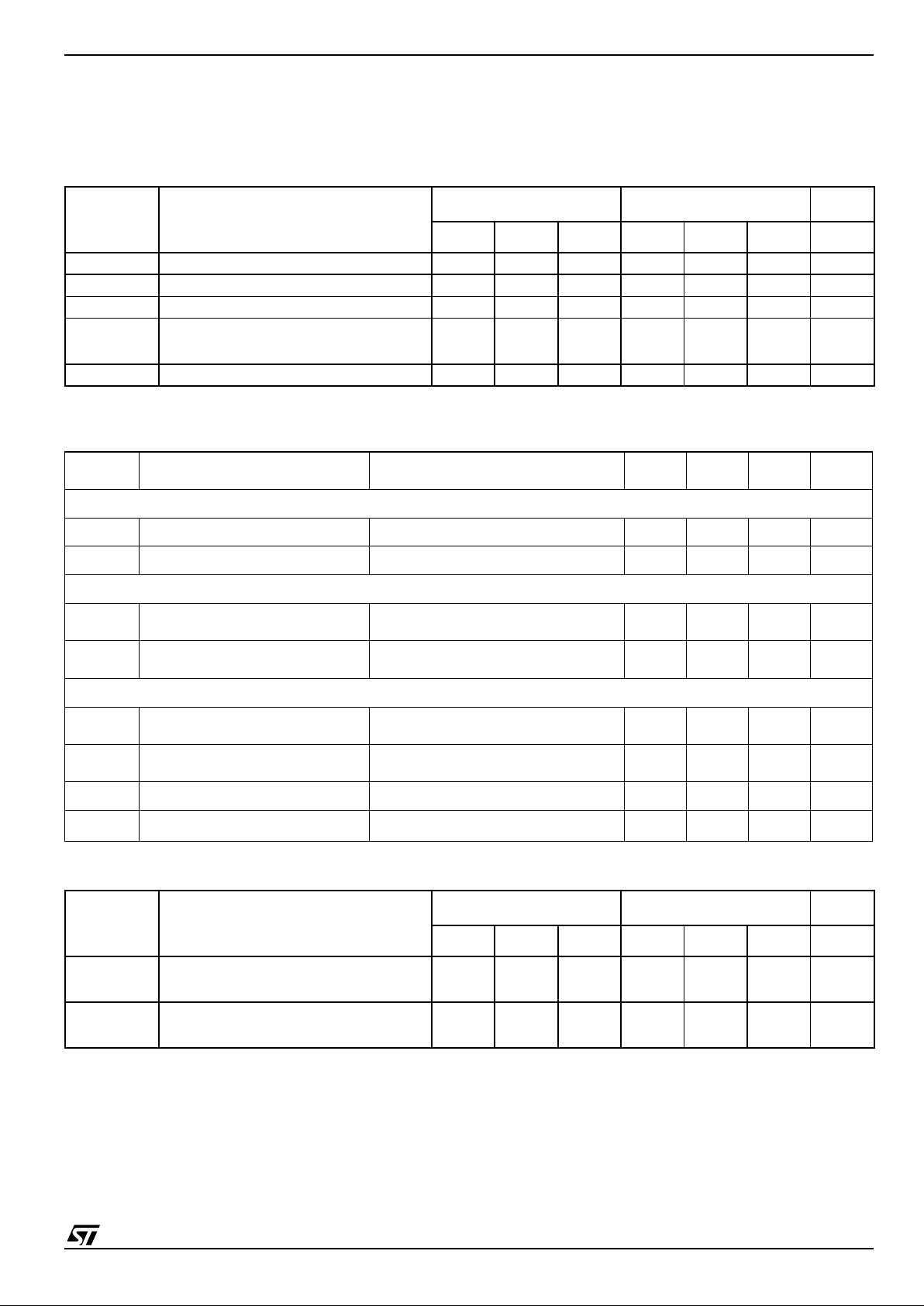
Static parameter: Integral Non Linearity
Fs=20MSPS; Icca= 30mA ; Fin=10M Hz
Static parameter: Integral Non Linearity
Fs=40MSPS; Icca= 45mA ; Fin=10M Hz
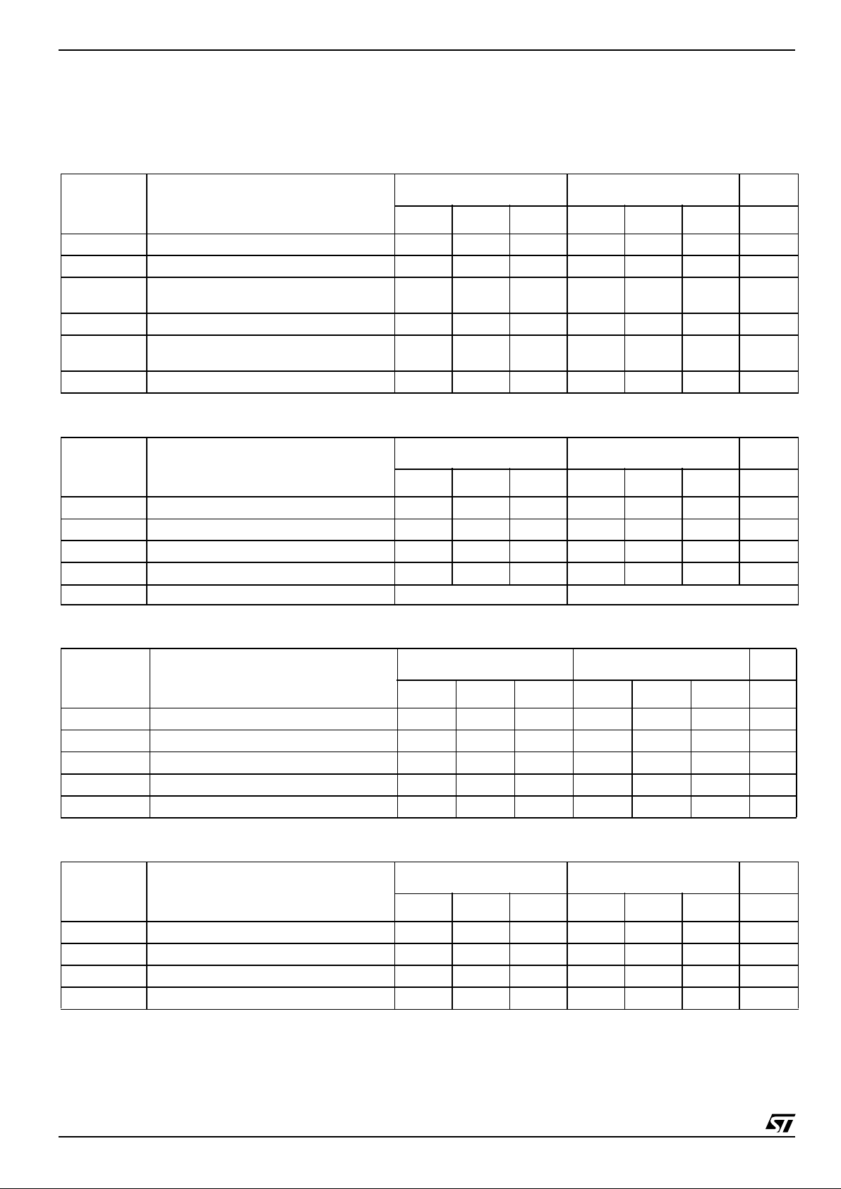
Static parameter: Differential Non Linearity
Fs=20MSPS; Icca= 30mA ; Fin=10M Hz
-1
-0.8
-0.6
-0.4
-0.2
0
0.2
0.4
0.6
0.8
1
0 200 400 600 800 1000
Ou t put Co de
INL (LSBs)
-2
-1.5
-1
-0.5
0
0.5
1
1.5
2
0 200 400 600 800 1000
Ou t put Co de
INL (LSBs)
-1
-0.8
-0.6
-0.4
-0.2
0
0.2
0.4
0.6
0.8
1
0 200 400 600 800 1000
Output Code
DNL (LSBs)

TSA1005
8/22
Static parameter: Differential Non Linearity
Fs=40MSPS; Icca=45mA; Fin=10MHz
Linearity vs. Fin
Fs=20MHz; Icca=30mA
Linearity vs. Fin
Fs=40MHz; Icca=45mA
Distortion vs. Fin
Fs=20MHz; Icca=30mA
Distortion vs. Fin
Fs=40MHz; Icca=45mA
-1
-0.8
-0.6
-0.4
-0.2
0
0.2
0.4
0.6
0.8
1
0 200 400 600 800 1000
Output Code
DNL (LSBs)
30
40
50
60
70
80
90
100
0204060
Fin (M Hz)
Dynamic parameters (dB)
5
6
7
8
9
10
11
12
ENOB (bits)
ENOB_I
SNR_I SINAD_I
SNR_Q SINAD_Q
ENOB_Q
30
40
50
60
70
80
90
100
0204060
Fin (M Hz)
Dynamic parameters (dB)
4
5
6
7
8
9
10
ENOB (bits)
ENOB_I
SNR_I SINAD_I
SNR_Q
SINAD_Q
ENOB_Q
-140
-120
-100
-80
-60
-40
-20
0
0204060
Fin (MHz)
Dynamic parameters (dBc)
SFDR_I
SFDR_Q
THD_I
THD_Q
-120
-100
-80
-60
-40
-20
0
0204060
Fin (MHz)
Dynamic parameters (dBc
)
SFDR_I
SFDR_Q
THD_I
THD_Q

TSA1005
9/22
Linearity vs. AVCC
Fs=20MSPS; Icca=30mA; Fin=5MHz
Linearity vs. AVCC
Fs=40MSPS; Icca=45mA; Fin=5MHz
Linearity vs. DVCC
Fs=20MSP S; Icca=30m A ; Fin=10 MHz
Distortion vs. AVCC
Fs=20MSP S; Icca=30 mA; Fin=5MHz
Distortion vs. AVCC
Fs=40MSP S; Icca=45 mA; Fin=5MHz
Distortion vs. DVCC
Fs=20MSP S; Icca=30mA; Fin=10MHz
50
55
60
65
70
75
80
2.25 2.35 2.45 2.55 2.65
AVCC (V)
Dynamic parameters (dB)
8
8.2
8.4
8.6
8.8
9
9.2
9.4
9.6
9.8
10
ENOB (bits)
SINAD_I
ENOB_I
SNR_I
SNR_Q
ENOB_Q
SINAD_Q
40
50
60
70
80
90
100
2.25 2.35 2.45 2.55 2.65
AVCC (V)
Dynamic parameters (dB)
5
5.5
6
6.5
7
7.5
8
8.5
9
9.5
10
ENOB (bits)
SINAD_I
ENOB_I
SNR_I
SNR_Q
ENOB_Q
SINAD_Q
50
55
60
65
70
75
80
2.25 2.35 2.45 2.55 2.65
DVCC (V)
Dynamic parameters (dB)
8
8.2
8.4
8.6
8.8
9
9.2
9.4
9.6
9.8
10
ENOB (bits)
SINAD_I
ENOB_I
SNR_ISNR_Q
ENOB_Q
SINAD_Q
-120
-110
-100
-90
-80
-70
-60
-50
-40
-30
2.25 2.35 2.45 2.55 2.65
AVCC (V)
Dynamic Parameters (dBc)
SFDR_Q
SFDR_I
THD_Q
THD_I
-120
-110
-100
-90
-80
-70
-60
-50
-40
-30
2.25 2.35 2.45 2.55 2.65
AVCC (V)
Dynamic Parameters (dBc)
SFDR_Q
SFDR_I
THD_Q
THD_I
-120
-110
-100
-90
-80
-70
-60
-50
-40
2.25 2.35 2.45 2.55 2.65
DVCC (V )
Dynamic Parameters (dBc)
SFDR_Q
SFDR_I
THD_Q
THD_I

TSA1005
10/22
Linearity vs. DVCC
Fs=40MSP S; Icca=45m A ; Fin=10 MHz
Linearity vs. VCCBI
Fs=20MSP S; Icca=30m A ; Fin=10 MHz
Linearity vs. VCCBI
Fs=40MSP S; Icca=45m A ; Fin=10 MHz
Distortion vs. DVCC
Fs=40MSP S; Icca=45mA; Fin=10MHz
Distortion vs. VCCBI
Fs=20MSPS; Icca=30mA; Fin=10MHz
Distortion vs. VCCBI
Fs=40MSPS; Icca=45mA; Fin=10MHz
40
50
60
70
80
90
100
2.25 2.35 2.45 2.55 2.65
DVCC (V)
Dynamic parameters (dB)
5
5.5
6
6.5
7
7.5
8
8.5
9
9.5
10
ENOB (bits)
SINAD_I
ENOB_I
SNR_I
SNR_Q
ENOB_Q
SINAD_Q
50
55
60
65
70
75
80
85
90
2.25 2.35 2.45 2.55 2.65
VCCBI (V)
Dynamic parameters (dB)
8
8.2
8.4
8.6
8.8
9
9.2
9.4
9.6
9.8
10
ENOB (bits)
SINAD_I
ENOB_I
SNR_I
SNR_Q
ENOB_Q
SINAD_Q
50
55
60
65
70
75
80
85
90
2.25 2.35 2.45 2.55 2.65
VCCBI (V)
Dynamic parameters (dB)
5
5.5
6
6.5
7
7.5
8
8.5
9
9.5
10
ENOB (bits)
SINAD_I
ENOB_I
SNR_I
SNR_Q
ENOB_Q
SINAD_Q
-120
-100
-80
-60
-40
-20
0
2.25 2.35 2.45 2.55 2.65
DVCC (V )
Dynamic Parameters (dBc)
SFDR_Q
SFDR_I
THD_QTHD_I
-120
-110
-100
-90
-80
-70
-60
-50
-40
2.25 2.35 2.45 2.55 2.65
VCCBI (V)
Dynamic Parameters (dBc)
SFDR_Q
SFDR_I
THD_Q
THD_I
-120
-110
-100
-90
-80
-70
-60
-50
-40
2.25 2.35 2.45 2.55 2.65
VCCBI (V)
Dynamic Parameters (dBc)
SFDR_Q
SFDR_I
THD_Q
THD_I

TSA1005
11/22
Linearity vs. VCCBE
Fs=20MSPS; Icca=30mA; Fin=10MHz
Linearity vs. VCCBE
Fs=40MSPS; Icca=45mA; Fin=10MHz
Linearity vs. Duty Cycle
Fs=20MH z; Icc a=30mA; Fin=5MH z
Distortion vs. VCCBE
Fs=20MSPS; Icca=30mA; Fin=10MHz
Distortion vs. VCCBE
Fs=40MSPS; Icca=45mA; Fin=10MHz
Distortion vs. Duty Cycle
Fs=20MH z; Icc a=30mA; Fin=5MH z
50
55
60
65
70
75
80
85
90
1.8 2.3 2.8 3.3
VCCBE (V)
Dynamic parameters (dB)
8
8.2
8.4
8.6
8.8
9
9.2
9.4
9.6
9.8
10
ENOB (bits)
SINAD_I
ENOB_I
SNR_Q
SNR_I
ENOB_Q
SINAD_Q
50
55
60
65
70
75
80
85
90
2.25 2.75 3.25
VCCBE (V)
Dynamic parameters (dB)
8
8.2
8.4
8.6
8.8
9
9.2
9.4
9.6
9.8
10
ENOB (bits)
SINAD_I
ENOB_I
SNR_Q
SNR_I
ENOB_Q
SINAD_Q
50
55
60
65
70
75
80
85
90
45 47 49 51 53 55
Positive Dut y Cycle (%)
Dynamic parameters (dB)
7
7.5
8
8.5
9
9.5
10
ENOB (bits)
SINAD_Q
SNR_Q
ENOB_Q
ENOB_I
SNR_I
SINAD_I
-100
-95
-90
-85
-80
-75
-70
-65
-60
1.8 2.3 2.8 3.3
VCCBE (V)
Dynamic Parameters (dBc)
SFDR_Q
SFDR_I
THD_Q
THD_I
-120
-110
-100
-90
-80
-70
-60
-50
-40
-30
2.25 2.75 3.25
VCCBE (V)
Dynamic Parameters (dBc)
SFDR_Q
SFDR_I
THD_Q
THD_I
-120
-110
-100
-90
-80
-70
-60
-50
-40
45 47 49 51 53 55
Positive Duty Cycle (%)
Dynamic paramet er s (dBc)
THD_Q
SFDR_Q
THD_I
SFDR_I

TSA1005
12/22
Linearity vs. Duty Cycle
Fs=40MHz; Icca=45mA ; Fin=5MHz
Distortion vs. Duty Cycle
Fs=40MHz; Icca=45mA ; Fin=5MHz
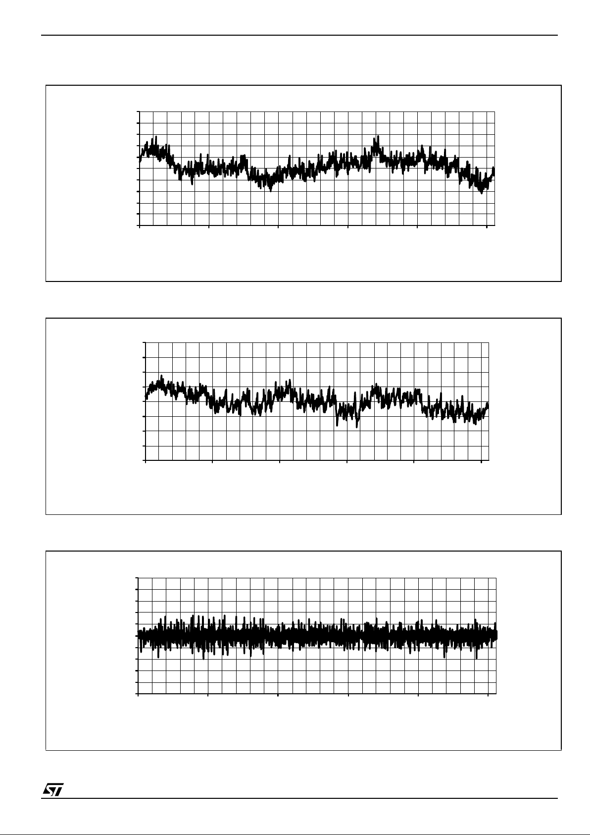
Single-tone 8K FFT at 24.8Msps - Q Channel
Fin=10MHz; Icca=30mA, Vin@-1dBFS
Single-tone 8K FFT at 39.7Msps - Q Channel
Fin=10MHz; Icca=45mA, Vin@-1dBFS
40
50
60
70
80
90
100
45 47 49 51 53 55
Positive Duty Cycle (%)
Dynamic parameters (dB)
5
5.5
6
6.5
7
7.5
8
8.5
9
9.5
10
ENOB (bits)
ENOB
SNR SINAD
-120
-110
-100
-90
-80
-70
-60
-50
-40
45 47 49 51 53 55
Positive Duty Cycle (%)
Dynamic parameters (dBc)
THD
SFDR
2468 1210
-20
-40
-60
-100
-80
-140
0
-120
Frequency (MHz)
Power spectrum (dB)
2468 121416 20
-20
-40
-60
-100
-80
-140
0
-120
Frequency (MHz)
Power spectrum (dB)
1810

TSA1005
13/22
DEFINITIONS OF SPECIF IED PARAMETERS
STATIC PARAMETERS
Static measurements are performed using a
histogram method with on a 2 MHz input signal,
sampled at 40 Msps, which is high enough to fully
characterize the test frequency response. An
input level of + 1 d BFS is required to saturate the
signal.
Differen t ial Non Li nearity (DNL )
The average deviation of any output code width
from the ideal code width of 1 LSB.
Integral Non linearity (INL)
An ideal conv erter present s a t ransf er f unct ion as
being the straight line from the starting code to the
ending code. The INL is the deviation for each
transition from this ideal curve.
DYNAMIC PARAMETERS
Dynamic measurements are performed by
spectral analysis, applied to an input sine wave of
various frequencies and sampled at 40 Msps.
The input level is -1 dBFS to m easure the linear
behavior of the converter. All the parameters are
given without correction for the full scale
amplitude performance except the calculated
ENOB parameter.
Spurious Free Dynamic Range (SFDR)
The ratio between the power of the worst spurious
signal (not always an harmonic) and the
amplitude of fundamental tone (signal power)
over the full Nyquist band. It is expressed in dBc.
T o tal Harmonic Distortion (THD)
The ratio o f the rm s s um of the first five harmo nic
distortion components to the rms value of the
fundamental line. It is expressed in dB.
Signal to Noise Ratio (SNR)
The ratio of the rms value of the fundamental
component to the rms sum of all other spectral
components in the Nyquist band (f
s
/2) excluding
DC, fundamental and the first five harmonics.
SNR is reported in dB.
Signal to Noise and Distortion Ratio (SINAD)
Similar ratio as for SNR but including the
harmonic distortion components in the noise
figure (not DC signal). It is expressed in dB.
From the SINAD, the Effective Number of Bits
(ENOB) can easily be deduced using the formula:
SINAD= 6.02 × ENO B + 1.76 dB .
When the applied signal is not Full Scale (FS), but
has an A
0
amplitude, the SINAD expression
becomes:
SINAD
2Ao
=SINAD
Full Scale
+ 20 log (2A0/FS)
SINAD
2Ao
=6.02 × ENOB + 1.76 dB + 20 log ( 2A0/FS)
The ENOB is expressed in bits.
Analog Input Bandwidth
The maximum analog input frequency at which
the spectral response of a full power signal is
reduced by 3 dB. Higher valu es can be achi eved
with sm a ller inp ut levels.
Effective Resolution Bandwidth (ERB)
The band of input signal frequencies that the ADC
is intended to convert without loosing linearity i.e.
the maximum analog input frequency at which the
SINAD is decreas ed by 3dB or the ENOB by 1/2
bit.
Pipeline delay
Delay between the initial sample of the analog
input and the availability of the corresponding
digital data output, on the output bus. Also called
data latency. It is expressed as a numb er of c lock
cycles.

TSA1005 APPLICATION NOTE
14/22
DETAILED INFORMATION
The TSA1005 is a dual-channel, 10-bit resolution
analog to digital converter based on a pipeline
structure and the latest deep sub micron CMOS
process to achieve the best performances in
terms of linearity and power consumption.
Each channel achieves 10-bit resolution through
the pipeline structure. A latency time of 7 clock periods is necessary to obtain the digi tized data on
the output bus.
The input signals are simultaneously sampled on
both channels on the rising edge of the clock. The
output data is valid on the rising edge of the c lock
for I channel and on the falling edge of the clock
for Q channel. The digital data out from the different stages must be time delayed depending on
their order of conversion. Then a digital data correction completes the processing and ensures the
validity of the ending codes on the output bus.
The structure has been specifically designed to
accept differential signals.
The TSA1005 is pin to pin compatible with the
dual 12bits/20Msps TSA1204 and the dual 12bits/
40Msps TSA1203.
COMPLEMENTARY FUNCTIONS
Some functionalities have been added i n order to
simplify as much as possible the application
board. These operational modes are described as
followed.
Output Enable (OEB)
When set to low level (VIL), all digital outputs
remain active and are in low impedance state.
When set to high level (VIH), all digital outputs
buffers are in high impedance state while the
converter goes on sampling. When OEB is set to a
low level again, the data a re then present on the
output with a very short Ton delay.
Therefore, this allows the chip select of the device.
The timing diagram summarizes this functionality.
In order to remain in the normal opera ting mode,
this pin should be grounded through a low value of
resistor.
SELECT
The digital data out from each ADC core are multiplexed together to share the same output bus.
This prevents from incre asing the num ber of p ins
and enables to k eep the same p ackage as single
channel ADC like TSA1002.
The selection of the chan nel information is done
through the "SELECT" pin. When set to high le vel
(VIH), the I chan nel data are present o n the bus
D0-D9. When set to low level (VIL), the Q channel
data are on the output bus D0-D9.
Connecting SELECT to CLK allows I and Q channels to be simultaneously present on D0-D9; I
channel on the rising edge of the clock and Q
channel on the falling edge of the clock. (see timing diagram page 2).
REFERENCES AND COMMON MODE
CONNECTION
VREFM must be always connec ted externally.
Internal reference and common mode
In the default configuration, the ADC operates with
its own reference and common mode voltages
generated by its internal bandgap. VREFM pins
are connected externally to the Analog Ground
while VREFP (respectively INCM) are set to their
internal voltage of 0.88V (respectively 0.46V). It is
recommended to decouple the VR EFP and I NCM
in order to minimize low and high frequency noise
(refer to Figure 1)
Figure 1: Internal reference and com mon mode
setting
TSA1005
VIN
VINB
VREFM
VREFP
330pF 4.7uF
10nF
INCM
330pF 4.7uF
10nF

TSA1005
15/22
External reference and common mode
Each of the voltages VREFP and INCM can be
fixed externally to better fit to the application
needs (Refer to table ’OPERATING
CONDITIONS’ page 4 for min/max values).
The VREFP, VREFM voltages set the analog
dynamic at the input of the converter that has a full
scale amplitude of 2*(VREFP-VREFM). Using
internal references, the dynamic range is 1.8V.
The INCM is the mid voltage of the analog input
signal.
It is possible to use an external referenc e voltage
device for specific applications requiring even
better linearity, accuracy or enhanced
temperature behavior.
Using the STMicroelectronics TS821 or
TS4041-1.2 Vref leads to optimum perform ances
when configured as shown on Figure 2.
Figure 2: External reference setting
DRIVING THE DIFFERENTIAL ANALOG
INPUTS
The TSA1005 has been designed to obtain
optimum performances when being differentially
driven. An RF transformer is a good way to
achieve such performances.
Figure 3 describes the schematics. The input
signal is fed to the primary of the transformer,
while the secondary drives both ADC inputs. The
common mode voltage of the ADC (INCM) is
connected to the center-tap of the secondary of
the transformer in order to bias the input signal
around this common voltage, internally set to
0.46V. It determines the DC component of the
analog signal. As being an high impedanc e input,
it acts as an I /O and can be externally driven t o
adjust this DC component. The INCM is
decoupled to maintain a low noise level on this
node. Our ev aluation board i s m ount ed with a 1: 1
ADT1-1WT transformer from Minicircuits. You
might also use a higher impedance ratio (1:2 or
1:4) to reduce the driving requirement on the
analog signal source.
Each analog input can drive a 1.4Vpp amplitude
input signal, so the resultant differential amplitude
is 2.8Vpp.
Figure 3: Differential input configuration with
transformer
Figure 4 represents the biasing of a differential
input signal in AC-coupled differential input
configuration. Both inputs VIN and VINB are
centered around the common m ode voltage, that
can be let internal or fixed externally.
Figure 4: AC-co upled differential input
Figure 5: AC-co upled Singl e-ended inp ut
1k
Ω
TSA1005
VIN
VINB
VREFM
VREFP
external
reference
VCCA
330pF 4.7uF
10nF
TS821
TS4041
TSA1005
VIN
VINB
INCM
50Ω
33pF
330pF
470nF
10nF
Analog so urce
1:1
ADT1-1
I or Q ch.
50Ω
10nF
TSA1005
VIN
VINB
INCM
33pF
100kΩ
100kΩ
50Ω
10nF
common
mode
50Ω
10nF
Signal source
TSA1005
VIN
VINB
INCM
33pF
100k Ω
100kΩ

TSA1005
16/22
Clock input
The TSA1005 perf ormance is very dependant on
your clock input accuracy, in terms of aperture
jitter; the use of low jitter crystal controlled
oscillator is recommended.
The duty cycle must be between 45% and 55%.
The clock power supplies must be separated from
the ADC output ones to avoid digital noise
modulation at the output.
It is recommended to always keep the circuit
clocked, even at the lowest specified sampling
frequency of 0.5Msps, before applying the sup ply
voltages.
Power co ns u m pt i on
So as to optimize both performance and power
consumption of the TSA1005 according the
sampling frequency , a resistor is placed betwe en
IPOL and the analo g Ground pins. Therefore, the
total dissipation is adjustable from 5Msps up to
40Msps.
The TSA1005 wil l combine highe st performances
and lowest consumption at 20Msp s when Rpol is
equal to 70kΩ, at 40M sps when Rpol is equal to
35kΩ. These values are nevertheless depe ndant
on application and environmen t.
At lower sampling frequency range, this value of
resistor may be adjusted in order to decrease the
analog current without any degradation of
dynamic performances.
The figure 6 sums up the relevant data.
Figure 6: analog current consumption
optimization depending on Rpol value
APPLICATION
Layo ut pre cautions
To use the ADC circuits in the best manner at high
frequencies, so me precautions h ave to be taken
for power supplies:
- First of all, the implementation of 4 separate
proper supplies and ground planes (analog,
digital, internal and external buffer ones) on the
PCB is recommended for high speed circuit
applications to provide low inductance and low
resistance common return.
The separation of the analog signal from the
digital part is mandatory to prevent noise from
coupling onto the input signal. The best
compromise is to connect from one part AGND,
DGND, GNDBI in a common point whereas
GNDBE must be isolated. Similarly, the power
supplies AVCC, DVCC and VCCBI must be
separated from the VCCBE one.
- Power supply bypass capacitors must be placed
as close as possible to the IC pins in order to
improve high frequency bypassing and reduce
harmonic distortion.
- Proper termination of all inputs and outputs must
be incorporated wi th output termination resistors;
then the amplifier load will be only resistive and
the stability of the amplifier will be improved. All
leads must be wide and as short as possible
especially for the analog input in order to decrease
parasitic capacitance and inductance.
- To keep the capacitive loading as low as
possible at digital outputs, short lead lengths of
routing are essential to minimize currents when
the output changes. To minimize this output
capacitance, buffers or latches close to the output
pins will relax this constraint.
- Choose component sizes as small as possible
(SMD).
Digital Inte rf ace app lic a t ion
Thanks to its wide external buffer power supply
range, the TSA1005 is perfectly suitable to plug i n
to 2.5V low voltage DSP s or digital interfaces as
well as to 3.3V ones.
Medical Imaging ap p l ic ation
Driven by the demand of the applications requiring
nowadays either portability or high degree of parallelism (or both), this product has been developed to satisfy medical imaging, and telecom infrastructures needs.
As a typical system diagram shows figure 10, a
narrow input beam of a coustic energy is sent into
a living body via the transducer and the energy reflected back is analyzed.
0
10
20
30
40
50
60
70
80
90
100
5 1525354555
Fs (MHz)
Icca (mA)
0
50
100
150
200
250
Rpol (kOhms)
RPOL
ICCA

TSA1005
17/22
Figure 7: Medical imaging application
The transducer is a p iezoele ctric ceramic such as
zirconium titanate. The whole array can reach up
to 512 channels.
The TX beam former, amplified by the HV TX
amps, delivers up to 100V amplitude excitation
pulses with phase and amplitude shifts.
The mux and T/R switc h is a two way input signal
transmitter/ output receiver.
To compensate for skin and tissues attenuation
effects, The Time Gain Com pens ation (T GC) am plifier is an exponential amplifier that enables the
amplification of low voltage signals t o the ADC input range. Differential output structure with low
noise and very high linearity are mandatory factors.
These applications need high speed, low power
and high performance ADCs . 10-12 bit resol ution
is necessary to lower the quant ification noise. As
multiple channels are used, a dual con verter is a
must for room saving issues.
The input signal is in the range of 2 to 20MHz
(mainly 2 to 7MHz) and the application uses mostly a 4 over-sampling ratio for Spurious Free Dynamic Range (SFDR) optimization.
The next RX beam form er and proces sing blocks
enable the anal ysis of the outputs channels versus the input beam.
EVAL1005/BA evaluation board
The EVAL1005/BA is a 4-layer board with high
decoupling and grounding level. The schematic of
the evaluation board is reported figure 11 and its
top overlay view figure 10.The characterizat ion of
the board has been made with a fully ADC
devoted test bench as shown on Figure 8. The
analog input signal must be filtered to be very
pure.
The dataready signal is the acquisition clock of the
logic analyzer.
The ADC digital outputs are latched by the octal
buffers 74LCX573.
All characterization measurements have been
made with:
- SFSR=1dB for static parameters.
- SFSR=-1dB for dynamic paramete rs.
Figure 8: Analog to Digital Converter characterization bench
Mux
and
TX
Proces
RX
AD
TGC amplifier
HV TX amps
Sine Wave
Generator
HP8644
ADC
evaluation
Pulse
Logic
Sine Wave
Generator
HP8644
HP8133
Vin
Clk
Data
Clk
PC

TSA1005
18/22
Operating conditions of the evaluation board:
Find below the connections to the board for the
power supplies and other pins:
Care should be taken for the evaluation board
considering the fact that the outputs of the converter are 2.5V/3.3V (VB2) tolerant whereas the
74LCX573 external buffers are operating up to
2.5V.
The ADC outputs on the connector J6 are D11
(MSB) to D2 (LSB).
Sin gle an d D if f e r e ntia l Inputs:
The ADC board comp onents are mounted to test
the TSA1005 with single analog input; the
ADT1-1WT transformer enables the differential
drive into the converter; in this configuration, the
resistors RSI6, RSI7, RSI8 for I channel (respectively RSQ6, RSQ7, RSQ8 for Q one) are connected as short circuits whereas RSI5, RSI9 (respectively RSQ5, RSQ9) are open circuits.
The other way is to test it via JI1 and JI1B differential inputs. So, the resistances RSI5, RSI9 for I
channel (respectively RSQ5, RSQ9 for Q one) are
connected as short circuits whereas RSI6, RSI7,
RSI8 (respectively RSQ6, RSQ7, RSQ8 for Q
one) are open circuits.
Grounding consi de ration
So as to bet ter reject n oise on the board, connec t
on the bottom overlay AG (AGND), DG(DGND),
GB1(GNDBI) together from one part, and
GB2(GNDBE) with GB3(GNDB3) from the other
part.
Mode select
So as to evaluate a single channel or the dual
ones, you have to connect on the board the
relevant position for the SELECT pin.
With the strap connected:
- to the upper connectors, the I channel at the output is se lec ted.
- horizontally, the Q channel at the output is selected.
- to the lower connectors, both c hannels are selected, relative to the clock edge.
Figure 9: mode se lect
Consumption adjustment
Before any characterization, care should be taken
to adjust the Rpol (Raj1) and therefore Ipol value
in function of your sampling frequency.
board
notation
connection
internal
voltage (V)
extern al
voltage (V)
AV AVCC
2.5
AG AGND
0
RPI REFPI
0.88 0.94 to 1.4
RMI REFMI
0 to 0.4
CMI INCMI
0.46 0 .2 to 1
RPQ REFPQ
0.88 0.94 to 1.4
RMQ REFMQ
0 to 0.4
CMQ INCMQ 0.46 0.2 to 1
DV DVCC
2.5
DG DGND
0
GB1 GNDBI
0
VB1 VCCBI
2.5
GB2 GNDBE
0
VB2 VCCBE
2.5/3.3
GB3 GNDB3
0
VB3 VCCB3
2.5
SELECT
DVCCDGNDCLK
I channel
Q channel
I/Q channels
SELECT
schematic board

TSA1005
19/22
Figure 10: Printed circuit of evaluation board.

TSA1005
20/22
Figure 11: TSA1005 Evaluation board schematic
RI1
50
R2
1K
R3
50
CI1
33pF
C2
330pF
C3
470nF
C4
10nF
CI8
330pF
CI9
10nF
CI10
470nF
CI11
330pF
CI12
10nF
CI13
470nF
C14 330pF
C15 10nF
C16 470nF
Raj1
200K
C17 330pF
C18 10nF
C19 470nF
J4
CLK
OEB1D02D13D24D35D46D57D68D79GND
10
LE
11
Q019Q118Q217Q316Q415Q514Q613Q7
12
VCC
20
U2
74LCX573
OEB1D02D13D24D35D46D57D68D79GND
10
LE
11
Q019Q118Q217Q316Q415Q514Q613Q7
12
VCC
20
U3
74LCX573
R11
47K
C25
330pF
C27
10nF
C28
470nF
+
C29
10µF
DO
D7D8D9
D10
D11
CI30
330pF
CI31
10nF
CI32
470nF
+
C34
47µF
+
C35
47µF
AVCC
VCCB2
VCCB1
C26 330pF
C39 10nF
C37 470nF
VCCB3
C33 330pF
C40 10nF
C38 470nF
C41
10µF
+
C42
47µF
CLK
D1D2D3D4D5
D6
C20 330pF
C21 10nF
C22 470nF
C23 10µ F+C36
47µF
1
4326
TI2
T2-AT1-1WT
JI1B
InIB
R5
50
J25
CKDATA
1
2
J27
CON2
RI19
50
S4
SW-SPST
VCCB1
GndB
1
VccB1
GndB
2
VccB2
GndB
3
VccB3
J17
BUFPOW
D0 GND
D1 GND
D2 GND (LSB)
D3 GND
D4 GND
D5 GND
D6 GND
D7 GND
D8 GND
D9 GND
D10 GND
D11 GND (MSB)
CLK GND
AVCC
C5
100nF
CI6
NM
VCCB2
C51 330pF
C52 10nF
C53 470nF
RSI5
0 NC
RSI6
0
RSI7
0
RSI80RSI9
0 NC
NM: non soudé analog input with transformer (default)
RS5 RS6 RS 7 RS 8 RS 9
C C C
C C
C C
single input
differential input
1
2
J26
CON2
CD3 330pF
CD2 10nF
CD1 470nF
RQ1
50
CQ1
33pF
CQ8
330pF
CQ9
10nF
CQ10
470nF
CQ11
330pF
CQ12
10nF
CQ13
470nF
CQ30
330pF
CQ31
10nF
CQ32
470nF
1
4326
TQ2
T2-AT1-1WT
JQ1B
InQB
RQ19
50
CQ6
NM
RSQ5
0 NC
RSQ6
0
RSQ70RSQ8
0
RSQ9
0 NC
AVCC
C10 330pF
C11 10nF
C13 470nF
C31 10µF+C32
47µF
DVCC
DVCC
DVcc
R21
0NM
R22
0NM
R23
0NM
R24
0NM
REFP
REFM
INCM
JI2
VREF I
REFP
REFM
INCM
JQ2
VREF Q
GND
VCC
JA
ANALOGIC
G
ND
V
CC
JD
DIGITAL
VCCB1
SW1
S5
SW-SPST
IN
Vcc
GNDS1
S2
D
U1
STG719
VCCB2
VCCB2
R12
47K
C43 10µF+C44
47µF
VCCB3
VCCB2 Switch S4 OEB Mode
Open Normal mode
Short High Impedance output mode
123456789
1011121314151617181920212223242526272829303132
J6
Switch S5
Open Normal mode
Short Test mode
AGND1INI2AGND3INBI4AGND5IPOL6AVCC7AGND8INQ9AGND10INBQ11AGND
12
REFPQ
13
REFMQ
14
INCMQ
15
AGND
16
AVCC
17
DVCC
18
DGND
19
CLK
20
SELECT
21
DGND
22
DVCC
23
GNDBI
24
GNDBE
25
VCCBE
26
D9(MSB)
27
D828D729D630D531D432D333D234D1
35
D0(LSB)
36
NC
37
NC
38
VCCBE
39
GNDBE
40
VCCBI
41
VCCBI
42
OEB
43
AVCC
44
AVCC
45
INCMI
46
REFMI
47
REFPI
48
Ra
ADC D UAL 10B

TSA1005
21/22
Figure 12: Printed circuit board - List of components
Name Foot pri nt Name Footprint Na me Footprint Name Part Footprint
Type
RSQ6
0
805 CD2 10nF 603 C26 330pF 603 CQ6 NC 805
RSQ7
0
805 C40 10nF 603 C20 330pF 603 CI6 NC 805
RSQ8
0
805 C39 10nF 603 C33 330pF 603 U2 74LCX573 TSSOP20
RSI6 0 805 CQ12 10nF 603 C25 330pF 603 U3 74LCX573 TSSOP20
RSI7 0 805 CQ9 10nF 603 CI1 33pF 603 U1 STG719 SOT23-6
RSI8
0
805 C52 10nF 603 CQ1 33pF 603 JA ANALOGIC connector
R3
47
603 C18 10nF 603 C34 47µF RB.1 J17 BUFPOW connector
R5
47
603 C21 10nF 603 C42 47µF RB.1 J25 CKDATA SMA
RQ19
47
603 C4 10nF 603 C35 47µF RB.1 J4 CLK SMA
RI1
47
603 C15 10nF 603 C44 47µF RB.1 J27 CON2 SIP2
RQ1
47
603 C27 10nF 603 C36 47µF RB.1 J26 CON2 SIP2
RI19 47 603 C11 10nF 603 C32 47µF RB.1 JD DIGITAL connector
RSI9 0NC 805 CI9 10nF 603 C37 470nF 805 JI1 InI SMA
RSQ5
0NC
805 CI12 10nF 603 CQ10 470nF 805 JI1B InIB SMA
RSQ9
0NC
805 CI31 10nF 603 C28 470nF 805 JQ1 InQ SMA
RSI5
0NC
805 CQ31 10nF 603 CI10 470nF 805 JQ1B InQB SMA
R24
0NC
805 CQ30 330pF 603 CQ32 470nF 805 SW1 SWITCH connector
R23
0NC
805 CI11 330pF 603 CQ13 470nF 805 S5 SW-SPST connector
R21 0NC 805 C51 330pF 603 CI32 470nF 805 S4 SW-SPST connector
R22 0NC 805 C2 330pF 603 C13 470nF 805 TI2 T2-AT1-1WT ADT
R2
1K
603 C17 330pF 603 C53 470nF 805 TQ2 T2-AT1-1WT ADT
R12
47K
603 CD3 330pF 603 C16 470nF 805 JI2 VREFI connector
R11
47K
603 C10 330pF 603 C3 470nF 805 JQ2 VREFQ connector
Raj1
200K
CQ8 330pF 603 C22 470nF 805 J6 32Pin
CQ11 330pF 603 CI13 470nF 805
C23
10µF
1210 CI8 330pF 603 C38 470nF 805
C41 10µF 1210 C14 330pF 603 CD1 470nF 805 NC: non soldered
C29 10µF 1210 CI 30 330pF 603 C19 470nF 805
VR5
trimmer
IDC-32
connector
Part
Type
Part
Type
Part
Type

TSA1005
22/22
PACKAGE MECHANICAL DATA
DIM.
mm. inch
MIN. TYP MAX. MIN. TYP. MAX.
A 1.6 0.063
A1 0.05 0.15 0.002 0.006
A2 1.35 1.40 1.45 0.053 0.055 0.057
B 0.17 0.22 0.27 0.007 0.009 0.011
C 0.09 0.20 0.0035 0.0079
D 9.00 0.354
D1 7.00 0.276
D3 5.50 0.216
e 0.50 0.020
E 9.00 0.354
E1 7.00 0.276
E3 5.50 0.216
L 0.45 0.60 0.75 0.018 0.024 0.030
L1 1.00 0.039
K 0˚3.5˚7˚ 0˚3.5˚7˚
TQFP48 MECHANICAL DATA
0110596/C
Information furnished is believed to be accurate and reliable. However, STMi croelectronics assumes no responsibility for the
consequences of use of such information nor for any infringement of patents or other rights of third parties which may result from
its use. No l i cense is granted by imp lica tion or otherwise under a ny patent or patent rig hts of STMicroelectronics. Specificat ions
mentioned in this pub lication are subject to change without notice. This publ ication supersedes and replaces all information
previously supplied. STMicroelectronics products are not authorized for use as critical components in life suppo rt devices or
systems without express written approval of STMicroelectronics.
The ST logo is a registered trademark of STMicroelectronics
© 2003 STMicroele ctronics - P r i n ted in Italy - A ll Rights Res er ved
STMicroelectronics GROUP OF COM PANIES
Austral i a - Brazil - Chi na - Finland - F rance - Germ any - Hong Kon g - India - Italy - Japan - Mal aysia - Malta - Morocco
Singapore - Spain - S weden - Switzerland - United Kingdom
http://www.st.com
 Loading...