


TS971
TS972
TS974
OUTPUT RAIL TO RAIL
VERYLOW NOISE OPERATIONAL AMPLIFIERS
.
RAILTO RAIL OUTPUT VOLTAGESWING
(±2.4V @ V
.
VERYLOW NOISE LEVEL: 4nV/√√Hz
.
ULTRALOWDISTORTION : 0.003%
.
HIGHDYNAMIC FEATURES(12MHz, 4V/µs)
.
OPERATINGRANGE : 2.7Vto 12V
.
ESD PROTECTION(2kV)
.
LATCH-UP IMMUNITY
.
AVAILABLEIN SOT23-5 MICROPACKAGE
= ±2.5V)
CC
DESCRIPTION
The TS97x family operational amplifiers is able to
operate with voltages as low as ±1.35Vandfeaturing output Rail to Rail signal swing. The TS97x
boasts characteristics that make them particularly
well suited for portableandbattery-suppliedequipment. Very low noise and low distortion characteristics make them ideal for audio
pre-amplification.
The TS971 is housed in the space-saving 5 pins
SOT23 package which simplifies theboard design
because of the ability to be placed everywhere
(outside dimensionsare 2.8mmx 2.9mm)
APPLICATIONS
.
Portableequipments(CD players, PDA)
.
Portablecommunications (cellphones, pagers)
.
Instrumentation& sensoring
.
Professionalaudio circuits
PIN CONNECTIONS (top view)
TS971ILT
Output
1
V
2
DD
Non-inverting input
Non-inve rting Input 1
Inve rting Inp ut 1
Non -inverting Input 1
3
TS971ID
1
N.C.
Inverting Inpu t1
Output1
2
-
+
3
V
4
DD
TS972IN-TS972ID-TS972IPT
1
-
2
+
3
V
45
DD
-
+
V
5
CC
Inverting input
4
N.C.
8
V
7
CC
6
Output 2
N.C.
5
V
8
CC
Output 2
7
6
Inve rting Input 2
Non-inverting Input2
ORDER CODES
Part
Number
TS971I -40, +125
TS972I -40, +125
TS974I -40, +125
N = Dual inLine Package (DIP)
D = Small Outline Package (SO) - also available in Tape & Reel
P = Thin Shrink Small Outline Package (TSSOP) - onlyavailable
in Tape & Reel (PT)
L = Tiny Package (SOT23-5) - only availablein Tape & Reel (LT)
August 1999
Temperature
Range
o
o
o
Package
NDPL
C ••K120
C •••
C •••
SOT23
Marking
TS974IN-TS974ID-TS974IPT
Output 1
1
Inverting Input 1
Non-invertingInput 1
Non-inverting Inp ut2
Inverting Input 2
V
Output 2
2
-
+
3
4
CC
5
+
-
6
7
14
13
-
+
12
11
10
+
-
9
8
Output 4
Inverting Input 4
Non-inverting Input4
V
DD
Non-inverting Input3
Inverting Input 3
Output 3
1/12
TS971-TS972-TS974
ABSOLUTEMAXIMUM RATINGS
Symbol Parameter Value Unit
V
CC
V
id
V
in
T
oper
T
stg
T
R
thjc
R
thja
ESD Human BodyModel 2 kV
Notes: 1. All voltages values, except differential voltage arewith respect to network ground terminal.
Supply Voltage - note 1 12 V
Differential Input Voltage - note2 ±V
CC
Input VoltageRange - note 3 -0.3 to12.3 V
Operating Free AirTemperature Range -40 to +125
Storage Temperature Range -65 to+150
Maximum JunctionTemperation 150
j
Thermal Resistance Junction to Case - note 4
SOT23-5
SO8
SO14
TSSOP8
TSSOP14
81
28
22
26
21
Thermal Resistance Junction to Ambient 256
Lead Temperature (soldering, 10sec) 260
2. Differential voltages are non-inverting input terminal with respect to the inverting input terminal.
3. The magniture of input and output voltages mustnever exceed V
4. Short-circuits can cause excessive heatingand destructive dissipation.
CC
+0.3V.
o
o
o
o
C/W
o
C/W
o
V
C
C
C
C
OPERATINGCONDITIONS
Symbol Parameter Value Unit
V
CC
V
icm
Supply Voltage Range 2.7 to 12 V
Common ModeInput VoltageRange VDD+ 1.15 to VCC- 1.15 V
2/12

TS971-TS972-TS974
ELECTRICAL CHARACTERISTICS
=2.5V,VDD= -2.5V, T
V
CC
Symbol Parameter Min. Typ. Max. Unit
V
DV
V
io
I
io
I
ib
icm
Input OffsetVoltage
T
min.<Tamb<Tmax.
Input OffsetVoltage Drift
io
= 0V, Vo=0V 5
V
icm
Input OffsetCurrent
= 0V, Vo= 0V 10 150
V
icm
Input BiasCurrent
= 0V, Vo=0V
V
icm
T
min.<Tamb<Tmax.
Common ModeInput VoltageRange -1.35 ±1.5 1.35 V
CMR Common Mode Rejection Ratio
= ±1.35V 60 85
V
icm
SVR Supply Voltage Rejection Ratio
V
= ±2V to ±3V 60 70
CC
A
V
V
I
source
I
sink
I
CC
vd
OH
OL
Large Signal VoltageGain RL=2kΩ 70 80 dB
High Level Output Voltage RL=2kΩ 2 2.4 V
Low Level OutputVoltage RL=2kΩ -2.4 -2 V
Output Source Current 1.5 mA
Output SinkCurrent 100 mA
Supply Current
Unity gain - no load 2 2.8
GBP Gain Bandwidth Product
f = 100kHz R
SR Slew Rate
A
=1,Vin= ±1V 2.8 4
V
∅m Phase Margin atUnity Gain R
Gm Gain Margin R
e
n
THD
Equivalent Input Noise Voltage
f = 100kHz
Total Harmonic Distortion
f = 1kHz,A
=25oC (unless otherwisespecified)
amb
=2kΩ,CL= 100pF 8.5 12
L
=2kΩ,CL= 100pF 60 Degrees
L
=2kΩ,CL= 100pF 10 dB
L
=-1 RL=10kΩ 0.003
V
15
7
200
200
750
1000
4
mV
µV/
nA
nA
dB
dB
mA
MHz
V/µs
nV
√Hz
o
C
%
3/12
TS971-TS972-TS974
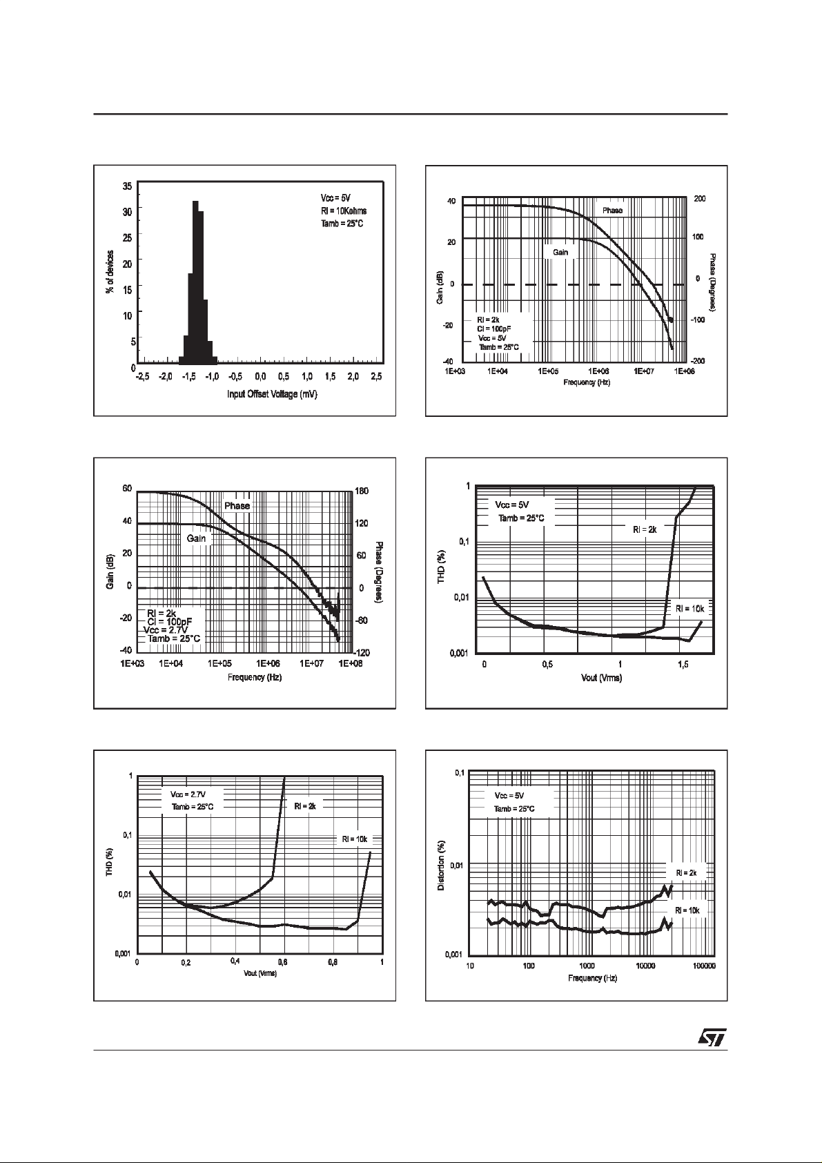
INPUT OFFSET VOLTAGEDISTRIBUTION
VOLTAGE GAIN & PHASEvs FREQUENCY
VOLTAGE GAIN& PHASE vs FREQUENCY
THDvs Vout
THD vs Vout THDvs FREQUENCY
4/12

TS971-TS972-TS974
NOISE VOLTAGEvs FREQUENCY
PHASE MARGIN vs Iout
GAIN BANDWIDTH PRODUCTvs Iout
PHASEMARGIN vsV
CC
PHASE MARGIN vs V
CC
GAIN MARGIN vs V
CC
5/12

TS971-TS972-TS974
TS972IN
PACKAGE MECHANICAL DATA
8 PINS- PLASTICDIP
Dimensions
A 3.32 0.131
a1 0.51 0.020
B 1.15 1.65 0.045 0.065
b 0.356 0.55 0.014 0.022
b1 0.204 0.304 0.008 0.012
D 10.92 0.430
E 7.95 9.75 0.313 0.384
e 2.54 0.100
e3 7.62 0.300
6/12
Min. Typ. Max. Min. Typ. Max.
Millimeters Inches

TS971ID - TS972ID
PACKAGE MECHANICAL DATA
8 PINS- PLASTICMICROPACKAGE (SO)
TS971-TS972-TS974
Dimensions
A 1.75 0.069
a1* 0.1 0.25 0.004 0.010
a2 1.65 0.065
a3 0.65 0.85 0.026 0.033
b 0.35 0.48 0.014 0.019
b1 0.19 0.25 0.007 0.010
C 0.25 0.5 0.010 0.020
c1 45
D 4.8 5.0 0.189 0.197
E 5.8 6.2 0.228 0.244
e 1.27 0.050
e3 3.81 0.150
F 3.8 4.0 0.150 0.157
L 0.4 1.27 0.016 0.050
M 0.6 0.024
S8
* coplanaritybetween allthe leads : 0.1mm
Min. Typ. Max. Min. Typ. Max.
Millimeters Inches
o
(typ.)
o
(max.)
7/12

TS971-TS972-TS974
TS972IPT
PACKAGE MECHANICAL DATA
8 PINS- THINSHRINK SMALL OUTLINE PACKAGE(TSSOP)
Dim.
Min. Typ. Max. Min. Typ. Max.
Millimeters Inches
A 1.20 0.05
A1 0.05 0.15 0.01 0.006
A2 0.80 1.00 1.05 0.031 0.039 0.041
b 0.19 0.30 0.007 0.15
c 0.09 0.20 0.003 0.012
D 2.90 3.00 3.10 0.114 0.118 0.122
E 6.40 0.252
E1 4.30 4.40 4.50 0.169 0.173 0.177
e 0.65 0.025
k0
o
o
8
o
0
l 0.50 0.60 0.75 0.09 0.0236 0.030
8/12
o
8

TS974IN
PACKAGE MECHANICAL DATA
14 PINS- PLASTICDIP
TS971-TS972-TS974
Dim.
a1 0.51 0.020
B 1.39 1.65 0.055 0.065
b 0.5 0.020
b1 0.25 0.010
D 20 0.787
E 8.5 0.335
e 2.54 0.100
e3 15.24 0.600
Min. Typ. Max. Min. Typ. Max.
Millimeters Inches
9/12

TS971-TS972-TS974
TS974ID
PACKAGE MECHANICAL DATA
14 PINS- PLASTIC MICROPACKAGE(SO)
Dim.
A 1.75 0.069
a1 0.1 0.2 0.004 0.008
a2 1.6 0.063
b 0.35 0.46 0.014 0.018
b1 0.19 0.25 0.007 0.010
C 0.5 0.020
c1 45
D 8.55 8.75 0.336 0.334
E 5.8 6.2 0.228 0.244
e 1.27 0.050
e3 7.62 0.300
F 3.8 4.0 0.150 0.157
G 4.6 5.3 0.181 0.208
L 0.5 1.27 0.020 0.050
M 0.68 0.027
S8
10/12
Min. Typ. Max. Min. Typ. Max.
Millimeters Inches
o
(typ.)
o
(max.)

TS974IPT
PACKAGE MECHANICAL DATA
14 PINS- THINSHRINK SMALL OUTLINE PACKAGE(TSSOP)
TS971-TS972-TS974
Dim.
Min. Typ. Max. Min. Typ. Max.
Millimeters Inches
A 1.20 0.05
A1 0.05 0.15 0.01 0.006
A2 0.80 1.00 1.05 0.031 0.039 0.041
b 0.19 0.30 0.007 0.15
c 0.09 0.20 0.003 0.012
D 4.90 5.00 5.10 0.192 0.196 0.20
E 6.40 0.252
E1 4.30 4.40 4.50 0.169 0.173 0.177
e 0.65 0.025
k0
o
o
8
o
0
l 0.50 0.60 0.75 0.09 0.0236 0.030
o
8
11/12

TS971-TS972-TS974
TS971ILT
PACKAGE MECHANICAL DATA
5 PINS-TINYPACKAGE (SOT23)
A
E
A2
Dim.
D
E1
Millimeters Inches
Min. Max. Min. Max.
b
A1
L
C
A 0.90 1.45 0.034 0.057
A1 0 0.15 0.006
A2 0.90 1.30 0.034 0.051
b 0.35 0.50 0.013 0.020
C 0.09 0.20 0.003 0.008
D 2.80 3.00 0.110 0.118
E 2.60 3.00 0.102 0.118
E1 1.50 1.75 0.059 0.069
L 0.10 0.60 0.003 0.024
Information furnished is believed to be accurate and reliable. However, STMicroelectronics assumes no responsibility for the
consequences of use ofsuch information nor forany infringement of patentsor other rights of third parties which may resultfrom
its use. No license is granted by implication or otherwise under any patent orpatent rights of STMicroelectronics. Specifications
mentioned in this publication are subject to change without notice. This publication supersedes and replaces all information
previously supplied.STMicroelectronicsproducts arenot authorized for useas criticalcomponents inlifesupportdevicesorsystems
without express written approval of STMicroelectronics.
Australia - Brazil -China - Finland - France - Germany - HongKong - India - Italy - Japan -Malaysia - Malta - Morocco
The ST logo is a trademark of STMicroelectronics
1999 STMicroelectronics – Printed in Italy –AllRights Reserved
STMicroelectronicsGROUP OF COMPANIES
Singapore - Spain - Sweden - Switzerland- United Kingdom- U.S.A.
http://www.st.com
12/12
 Loading...