

Datasheet TS934IDT, TS934ID, TS934, TS932IN, TS932IDT Datasheet (SGS Thomson Microelectronics)
...
1/14
■ RAIL TO RAIL OUTPUT VOLTAGE SWING
■ MICROPOWER CONSUMPTION (20µA)
■ SINGLE SUPPLY OPERATION (2.7V to 10V
■ LOW OFFSET (2mV max for TS93xB)
■ CMOS INPUTS
■ ULTRA LOW INPUT BIAS CURRENT (1pA)
■ ESD PROTECTION (2kV)
■ LATCH-UP IMMUNITY (Class A)
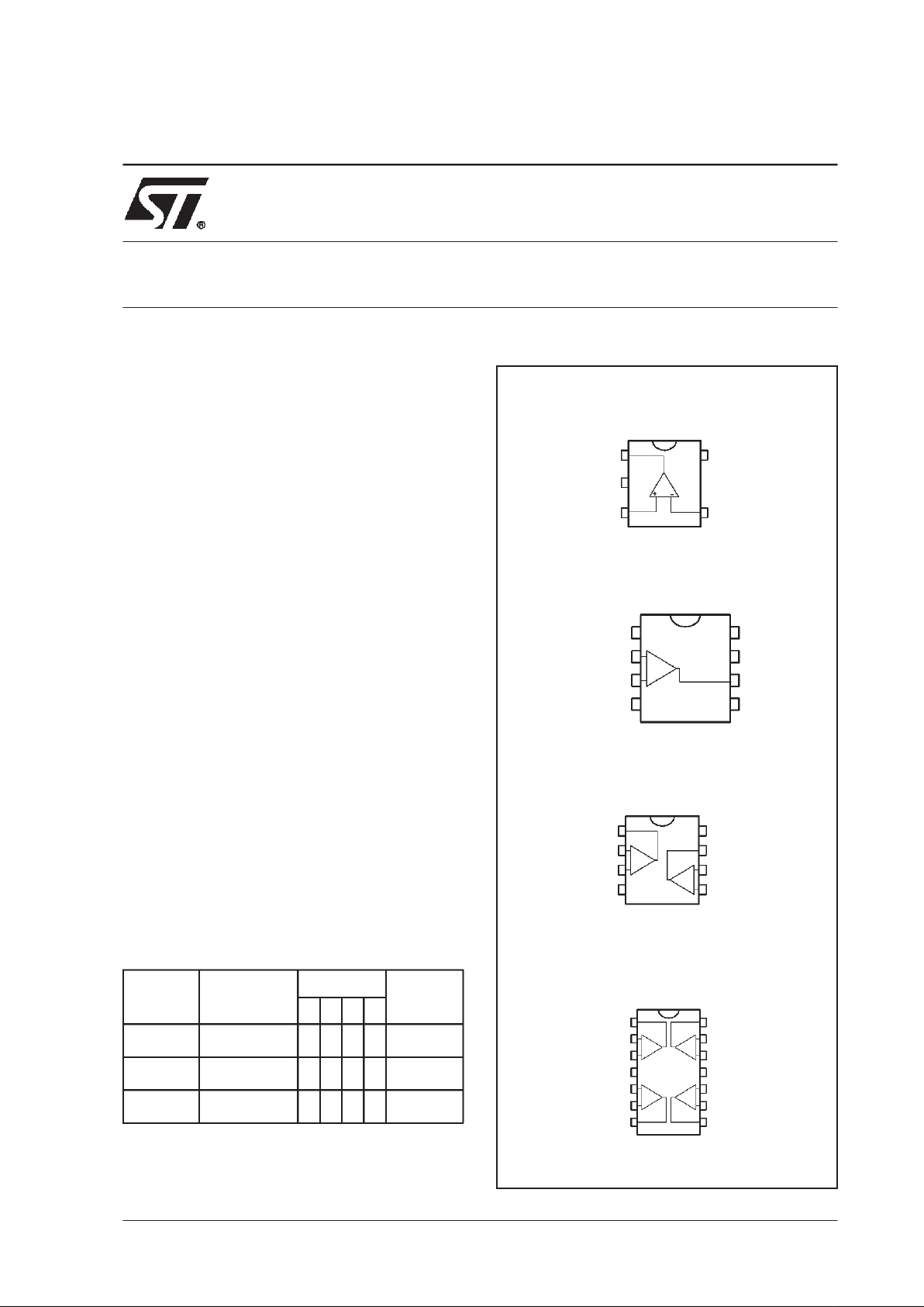
■ AVAILABLE IN SOT23-5 MICROPACKAGE
DESCRIPTION
The TS93x (Single, Dual & Quad) is Operational
Amplifier able to operate with voltage as low as
2.7V and to reach 2.9Vpp of output swing with
RL= 100kΩ when supplied @ 3V. Offering a typi-
cal consumption of only 20µA, it is particularly
well-suited for every kind of battery-supplied applications.
The TS93x is housed in the space-saving 5 pins
SOT23-5 package which simplifies the board design because of the ability to be placed everywhere (outside dimensions are : 2.8mm x 2.9mm).
APPLICATION
■ Battery-powered systems
■ Portable communication systems
■ Alarm, smoke detectors
■ Instrumentation & sensoring
■ PH Meter
■ Digital scales
ORDER CODE
N=Dual in Line Package (DIP)
D=Small Outline Package (SO) - also available in Tape & Reel (DT)
P=Thin Shrink Small Outline Package (TSSOP) - only available
in Tape & Reel (PT)
L=Tiny Package (SOT23-5) - only available in Tape & Reel (LT)
PIN CONNECTIONS (top view)
Part
Number
Temperature
Range
Package
SOT23
Marking
NDPL
TS931I
TS931A/BI
-40, +85°C
•
•
••K205
K206/207
TS932I
TS932A/BI
-40, +85°C
•••
•
TS934I
TS934A/BI
-40, +85°C
•••••
•
1
2
3
4
5
Inverting input
Non-inverting input
Output
V
DD
V
CC
1
2
3
4
5
6
7
8
-
+
Inve rting Input 1
N.C.
Non-inve rting Inp ut 1
V
DD
V
CC
Output 2
N.C.
N.C.
Inverting Input 2
Non-inve rting Input 2
Non-inve rting Input1
DD
V
1
2
3
4
8
5
6
7
9
10
11
12
13
14
CC
V
Outp ut 3
Outp ut 4
Non-inve rting Input4
Inverting Input 4
Non-inve rting Input3
Inverting Input 3
-
+
+
-
+
-
+
Output 1
Inve rting Input 1
Output 2
1
2
3
45
6
7
8
-
+
-
+
Inve rting Input 1
Output 1
Non-inve rting Input 1
V
DD
V
CC
Output 2
Inverting Input 2
Non-inve rting Input 2
TS931ILT
TS934IN-TS934ID-TS934IDT-TS934IPT
TS931ID-TS931IDT
TS932IN-TS932ID-TS932IDT
TS931
TS932
TS934
OUTPUT RAIL TO RAIL
MICROPOWER OPERATIONAL AMPLIFIERS
May 2000
TS931-TS932-TS934
2/14
ABSOLUTE MAXIMUM RATINGS
OPERATING CONDITIONS
Symbol Parameter Value Unit
V
CC
Supply voltage
1)
12 V
V
id
Differential Input Voltage
2)
±12 V
V
in Input Voltage Range
3)
-0.3 to 12.3 V
T
oper
Operating Free Air Temperature Range -40 to + 85 °C
T
std
Storage Temperature Range -65 to +150 °C
T
j
Maximum Junction Temperature 150 °C
R
thjc
Thermal Resistance Junction to Case
4)
SOT23-5
DIP8
DIP14
SO8
SO14
TSSOP8
TSSOP14
81
42
32
28
22
26
21
°C/W
R
thja
Thermal Resistance Junction to Ambient - SOT23-5 256 °C/W
ESD Human Body Model 2 kV
Latch-up Immunity Class A
Lead Temperature (soldering, 10sec) 260 °C
1. All voltages values, except differential voltage are with respect to network terminal.
2. Differential voltages are non-inverting input terminal with respect to the inverting input terminal.
3. The magnitude of input and output voltages must never exceed V
CC
+0.3V.
4. Short-circuits can cause excessive heating and destructive dissipation.
Symbol Parameter Value Unit
V
CC
Supply Voltage 2.7 to 10 V
V
icm
Common Mode Input Voltage Range
V
ee
- 0.2 to VCC- 1.5
V

TS931-TS932-TS934
3/14
ELECTRICAL CHARACTERISTICS
VCC= +3V,Vee= 0V,
T
amb
=25°C (unless otherwise specified)
Symbol Parameter Min. Typ. Max. Unit
V
io
Input Offset Voltage
TS931/2/4
TS931/2/4A
TS931/2/4B
10
5
2
mV
∆V
io
Input Offset Voltage Drift 3 µV/°C
I
io
Input Offset Current
1)
1. Maximum values including unavoidable inaccurates of the industrial test.
1 100 pA
I
ib Input Bias Current
1)
1 150 pA
CMR
Common Mode Rejection Ratio
0 ≤ V
icm
≤ VCC- 1.7
85 dB
SVR
Supply Voltage Rejection Ratio
2)
2. VCChas a 0.2V variation.
85 dB
A
vd
Large Signal Voltage Gain
V
O
= 2Vpp RL=1MΩ
R
L
= 100kΩ
120
106
dB
V
OH
High Level Output Voltage
V
ID
= 100mV RL= 100kΩ
2.95
V
V
OL
Low Level Output Voltage
V
ID
= -100mV RL= 100kΩ
50
mV
I
o
Output Source Current
V
ID
= 100mV, VO=V
DD
Output Sink Current
V
ID
= -100mV,VO=V
CC
1.5
1.5
mA
I
CC
Supply Current (per amplifier)
A
VCL
= 1, no load
20 31
µA
GBP
Gain Bandwith Product R
L
= 100kΩ,CL= 50pF
100 kHz
SR
Slew Rate R
L
= 100kΩ,CL= 50pF
50 V/ms
φm
Phase Margin C
L
= 50pF
65 Degrees
en Input Voltage Noise 75 nV/√Hz

TS931-TS932-TS934
4/14
ELECTRICAL CHARACTERISTICS
VCC= +5V,Vee= 0V,
T
amb
=25°C (unless otherwise specified)
Symbol Parameter Min. Typ. Max. Unit
V
io
Input Offset Voltage
TS931/2/4
TS931/2/4A
TS931/2/4B
10
5
2
mV
∆V
io
Input Offset Voltage Drift 3 µV/°C
I
io Input Offset Current
1)
1 100 pA
I
ib Input Bias Current
1)
1 150 pA
CMR
Common Mode Rejection Ratio
0 ≤ V
icm
≤ VCC- 1.7
85 dB
SVR
Supply Voltage Rejection Ratio
2)
85 dB
A
vd
Large Signal Voltage Gain
V
O
= 4Vpp RL=1MΩ
R
L
= 100kΩ
120
112
dB
V
OH
High Level Output Voltage
V
ID
= 100mV RL= 100kΩ
4.95
V
V
OL
Low Level Output Voltage
V
ID
= -100mV RL= 100kΩ
50
mV
I
o
Output Source Current
V
ID
= 100mV, VO=V
DD
Output Sink Current
V
ID
= -100mV,VO=V
CC
5
5
mA
I
CC
Supply Current (per amplifier)
A
VCL
= 1, no load
20 33
µA
GBP
Gain Bandwith Product R
L
= 100KΩ,CL= 50pF
100 kHz
SR
Slew Rate R
L
= 100KΩ,CL= 50pF
50 V/ms
φm
Phase Margin C
L
= 50pF
65 Degrees
en Input Voltage Noise 76 nV/√Hz
1. Maximum values including unavoidable inaccurates of the industrial test.
2. VCChas a 0.2V variation.
TS931-TS932-TS934
5/14
Temperature(°C)
Input Offset Voltage Drift ( V)µ
-40 -20 0 20 40 60 80
-150
-100
-50
0
50
Vcc=5V
024681012
0
2
4
6
8
10
12
SupplyVoltage (V)
Vid=-100mV
Vid=+100mV
Supply Current ( A)µ
Tamb=25 °CTamb=25°C
-40 -20 0 20 40 60 80
-6
-4
-2
0
2
4
6
Isink,Vcc=3V
Isink,Vcc=5V
Isource,Vcc=5V
Output Short-Circuit Current (mA)
Temperature (°C)
Isource,Vcc=3V
024681012
0
2
4
6
8
10
12
14
16
18
20
SupplyVoltage (V)
Supply Current ( A)µ
Tamb=25°CTamb=25°C
Temperature(°C)
Supply Current ( A)µ
-40 -20 0 20 40 60 80
16
17
18
19
20
21
Vcc from 2.7V to 10V
246810
-30
-20
-10
0
10
20
30
Source
Sink
Tamb=25°C
Output Short-Circuit Current (mA)
SupplyVoltage (V)

TS931-TS932-TS934
6/14
0123
-2
-1.5
-1
-0.5
0
0.5
1
T=+85°C
T=+25°C
T=-40°C
T=+85°C
T=+25°C
T=-40°C
Output Shor t-Circuit Current (mA)
OutputVoltage (V)
Vcc=2.7V
Sink
Source
Output Short-Circuit Current (mA)
OutputVoltage(V)
T=+85°C
T=+25°C
T=-40°C
T=+85°C
T=+25°C
T=-40°C
Source
Sink
012345
-6
-4
-2
0
2
4
6
Vcc=5V
246810
1
2
5
10
20
50
100
200
500
RL = 10k Ω
RL tied to VDD
SINGLE SUPPLY
Vid = +100mV
RL = 100kΩ
RL = 1M
Ω
Voltagereferenced to Vcc (mV)
Supply Voltage(V)
0 0.5 1 1.5 2 2.5 3
-2
-1
0
1
Output Short-Circuit Current (mA)
OutputVoltage (V)
T=-40°C
T=+85°C
T=+25°C
T=-40°C
Sink
Vcc=3V
Source
T=+85°C
T=+25°C
Output Short-Circuit Current (mA)
Output Voltage (V)
T=+85°C
T=+25°C
T=-40°C
T=+85°C
T=-40°C
Source
Sink
0246810
-30
-20
-10
0
10
20
30
Vcc=10V
T=+25°C
RL = 10k Ω
RL = 100k Ω
RL = 1M
Ω
Voltagereferenced to VDD (mV)
Supply Voltage(V)
246810
1
2
5
10
20
50
100
200
500
RL tied to Vcc
SINGLE SUPPLY
Vid = -100mV

TS931-TS932-TS934
7/14
100 200 500 1,000 2,000 5,000 10,000 20,000 50,000 100,000
0
10
20
30
40
50
60
70
60
80
100
120
140
160
180
Frequency (Hz)
Gain (dB)
Phase (°)
Gain
Phase
RL = 100k
CL = 50 pF
Vcc = 3V & 5V
20 50 100 200 500 1,000 2,000 5,000 10,000
0
0.2
0.4
0.6
0.8
1
RL=100k
Gain = +2
Vcc=5V
Vo=4Vpp
Vcc=3V
Vo=2Vpp
Frequency (Hz)
Distortion (%)
10 30 100 300 1,000 3,000 10,000
0
20
40
60
80
100
Frequency (Hz)
Equivalent Noise Voltage(nV/ Hz)√
Vcc = 2.7V
Rs = 100
Tamb= 25°C
100 200 500 1,000 2,000 5,000 10,000 20,000 50,000 100,000
0
10
20
30
40
50
60
70
40
60
80
100
120
140
160
180
Frequency (Hz)
Gain (dB)
Phase (°)
Gain Phase
RL = 100k
CL = 100 pF
Vcc = 3V & 5V
12345
0
0.5
1
1.5
2
Output Voltage(Vpp)
Distortion (%)
RL=100k
Gain = +2
Vcc=3V
Vcc=5V
F = 100Hz
100 300 1,000 3,000 10,000 30,000 100,000 300,000 1,000,000
-75
-70
-65
-60
-55
-50
-45
-40
Frequency (Hz)
SupplyVoltage Rejection (dB)
Vcc = 5V
Gain = +1

TS931-TS932-TS934
8/14
INPUT
0V
OUTPUT
0V
0 5 10 15 20 25 30 35 40 45 50
Time ( s)µ
Voltage (50mV/div)
Vcc = 5V
Gain = +1
RL =100k
CL =50pF
0 100 200 300 400 500
Voltage(1V/div)
Time ( s)µ
Vcc = 5V
Gain = +1
RL = 100k
CL = 50pF
INPUT
0V
OUTPUT
0V

TS931-TS932-TS934
9/14
TS932IN
PACKAGE MECHANICAL DATA
8 PINS - PLASTIC PACKAGE
Dim.
Millimeters Inches
Min. Typ. Max. Min. Typ. Max.
A 3.32 0.131
a1 0.51 0.020
B 1.15 1.65 0.045 0.065
b 0.356 0.55 0.014 0.022
b1 0.204 0.304 0.008 0.012
D 10.92 0.430
E 7.95 9.75 0.313 0.384
e 2.54 0.100
e3 7.62 0.300
e4 7.62 0.300
F 6.6 0260
i 5.08 0.200
L 3.18 3.81 0.125 0.150
Z 1.52 0.060

TS931-TS932-TS934
10/14
TS931ID - TS932ID
PACKAGE MECHANICAL DATA
8 PINS - PLASTIC MICROPACKAGE (SO)
Dim.
Millimeters Inches
Min. Typ. Max. Min. Typ. Max.
A 1.75 0.069
a1 0.1 0.25 0.004 0.010
a2 1.65 0.065
a3 0.65 0.85 0.026 0.033
b 0.35 0.48 0.014 0.019
b1 0.19 0.25 0.007 0.010
C 0.25 0.5 0.010 0.020
c1 45° (typ.)
D 4.8 5.0 0.189 0.197
E 5.8 6.2 0.228 0.244
e 1.27 0.050
e3 3.81 0.150
F 3.8 4.0 0.150 0.157
L 0.4 1.27 0.016 0.050
M 0.6 0.024
S8°(max.)

TS931-TS932-TS934
11/14
TS934IN
PACKAGE MECHANICAL DATA
14 PINS - PLASTIC PACKAGE
Dim.
Millimeters Inches
Min. Typ. Max. Min. Typ. Max.
a1 0.51 0.020
B 1.39 1.65 0.055 0.065
b 0.5 0.020
b1 0.25 0.010
D 20 0.787
E 8.5 0.335
e 2.54 0.100
e3 15.24 0.600
F 7.1 0.280
i 5.1 0.201
L 3.3 0.130
Z 1.27 2.54 0.050 0.100

TS931-TS932-TS934
12/14
TS934ID
PACKAGE MECHANICAL DATA
14 PINS - PLASTIC MICROPACKAGE (SO)
Dim.
Millimeters Inches
Min. Typ. Max. Min. Typ. Max.
A 1.75 0.069
a1 0.1 0.2 0.004 0.008
a2 1.6 0.063
b 0.35 0.46 0.014 0.018
b1 0.19 0.25 0.007 0.010
C 0.5 0.020
c1 45° (typ.)
D (1) 8.55 8.75 0.336 0.344
E 5.8 6.2 0.228 0.244
e 1.27 0.050
e3 7.62 0.300
F (1) 3.8 4.0 0.150 0.157
G 4.6 5.3 0.181 0.208
L 0.5 1.27 0.020 0.050
M 0.68 0.027
S8°(max.)
Note : (1) D and F do not include mold flash or protrusions - Mold flash or protrusions shall not exceed 0.15mm (.066 inc) ONLY FOR DATA BOOK.
D
M
F
14
1
7
8
b
e3
e
E
LG
C
c1
A
a2
a1
b1
s

TS931-TS932-TS934
13/14
TS934IPT
PACKAGE MECHANICAL DATA
14 PINS - THIN SHRINK SMALL OUTLINE PACKAGE
Dim.
Millimeters Inches
Min. Typ. Max. Min. Typ. Max.
A 1.20 0.05
A1 0.05 0.15 0.01 0.006
A2 0.80 1.00 1.05 0.031 0.039 0.041
b 0.19 0.30 0.007 0.15
c 0.09 0.20 0.003 0.012
D 4.90 5.00 5.10 0.192 0.196 0.20
E 6.40 0.252
E1 4.30 4.40 4.50 0.169 0.173 0.177
e 0.65 0.025
k0° 8°0° 8°
l 0.50 0.60 0.75 0.09 0.0236 0.030
c
E1
k
L
E
e
b
D
L1
A
A2
A1

TS931-TS932-TS934
14/14
Information furnished is believed to be accurate and reliable. However, STMicroelectronics assumes no responsibility for the
consequences of use of such information nor for any infring ement of patents or other rights of third parties which may resultfrom
its use. No license is granted by implication or otherwise under any patent or patent rights of STMicroelectronics. Specifications
mentioned in this publication are subject to change without notice. This publication supersedes and replaces all information
previously supplied. STMicroelectronics products are not authorized for use as critical components in life support devices or
systems withou texpress written approval of STMicroelectronics.
The ST logo is a registered trademark of STMicroelectronics
2000 STMicroelectronics - Printedin Italy - All Rights Reserved
STMicroelectronics GROUP OF COMPANIES
Australia - Brazil - China - Finland - France - Germany - Hong Kong - India - Italy - Japan - Malaysia - Malta - Morocco
Singapore - Spain - Sweden - Switzerland - United Kingdom
http://www.st.com
TS931ILT
PACKAGE MECHANICAL DATA
5 PINS - TINY PACKAGE (SOT23)
Dim.
Millimeters Inches
Min. Typ. Max. Min. Typ. Max.
A 0.90 1.20 1.45 0.035 0.047 0.057
A1 0 0.15 0.006
A2 0.90 1.05 1.30 0.035 0.041 0.051
B 0.35 0.40 0.50 0.014 0.016 0.020
C 0.09 0.15 0.20 0.004 0.006 0.008
D 2.80 2.90 3.00 0.110 0.114 0.118
D1 1.90 0.075
e 0.95 0.037
E 2.60 2.80 3.00 0.102 0.110 0.0118
F 1.50 1.60 1.75 0.059 0.063 0.069
L 0.10 0.5 0.60 0.004 0.014 0.024
K 0d 10d 0d 10d
L
C
E1
A2
A
A1
b
E
D
 Loading...