

SGS Thomson Microelectronics TS925IN, TS925ID, TS925 Datasheet
RAILTO RAIL HIGH OUTPUTCURRENT
.
RAILTO RAIL INPUTANDOUTPUT
.
LOW NOISE : 9nV/√√Hz
.
LOW DISTORTION
.
HIGHOUTPUTCURRENT : 80mA
(able to drive 32Ω loads)
.
HIGHSPEED : 4MHz,1.3V/µs
.
OPERATINGFROM2.7V TO 12V
.
LOW INPUT OFFSET VOLTAGE : 900µV max.
(TS925A)
.
ADJUSTABLE PHANTOM GROUND (VCC/2)
.
STANDBY MODE
.
ESD INTERNALPROTECTION :2kV
.
LATCH-UP IMMUNITY
.
MACROMODEL INCLUDED IN THIS
SPECIFICATION
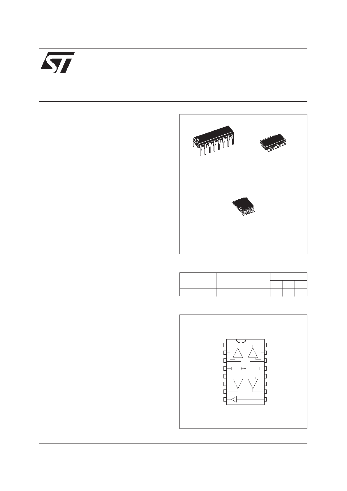
TS925
QUAD OPERATIONALAMPLIFIER
N
DIP16
(Plastic Package)
(Thin ShrinkSmall Outline Package)
(Plastic Micropackage)
P
TSSOP16
D
SO16
DESCRIPTION
The TS925 is a RAIL TO RAIL quad BiCMOS
operational amplifier optimized and fully specified
for 3V and 5V operation.
High output current allows lowload impedancesto
be driven. An internal low impedance PHANTOM
GROUND eliminates the need for an external reference voltage or biasingarrangement.
The TS925exhibitsavery lownoise,lowdistortion
and high output current making this device an
excellent choice for high quality, low voltage or
battery operatedaudio/telecomsystems.
The device is stable for capacitive loads up to
500pF.
When the STANDBY mode is enabled, the total
consumption drops to 6µA(V
APPLICATIONS
.
Headphoneamplifier
.
Soundcardamplifier, piezoelectric speaker
.
MPEGboards, multimediasystems,...
.
Cordless telephones and portable communication equipment
.
Line driver, buffer
.
Instrumentationwithlownoise askeyfactor
CC
= 3V).
ORDER CODES
Part Number Temperature Range
o
TS925I -40,+125
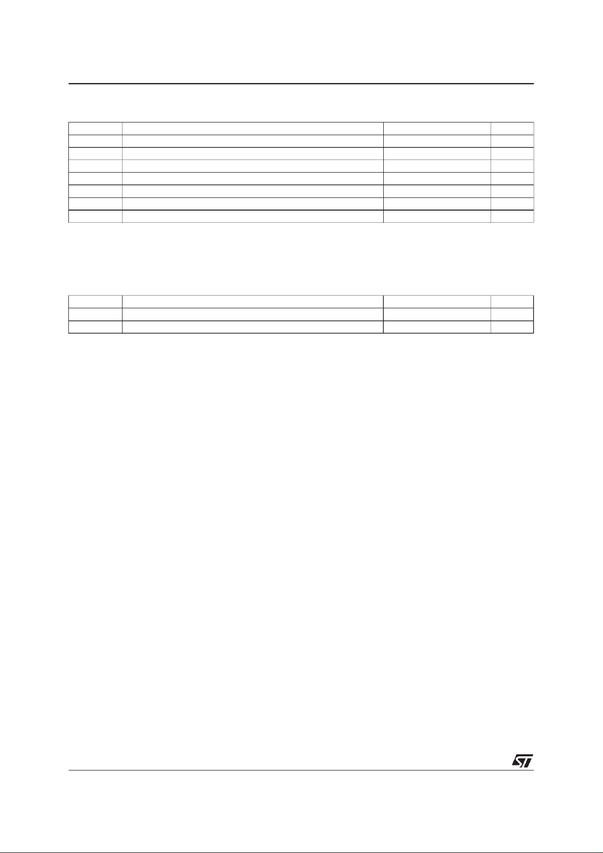
PIN CONNECTIONS
Output 1
1
Inverting
2
Input 1
Non-inve rting
Input 1
V
Non-inve rting
Input 2
Inverting
Input 2
Output 2
P hantom ground
+
CC
3
4
5
6
7
8
-
--
C •••
-
+
+
+
+
Package
NDP
16
Ou tput 4
Inve rting
15
Inpu t 4
Non-inverting
14
Inpu t 4
V
-
13
CC
Non-inverting
12
Inpu t 3
Inve rting
11
Inpu t 3
10
Ou tput 3
9
Stdby
March 1999
1/16
TS925
ABSOLUTE MAXIMUM RATINGS
Symbol Parameter Value Unit
V
CC
V
id
V
T
oper
T
R
thja
Notes : 1. All voltage values, except differential voltage are with respect to network ground terminal.
OPERATING CONDITIONS
Symbol Parameter Value Unit
V
CC
V
icm
Supply Voltage- (note 1) 14 V
Differential Input Voltage- (note 2) ± 1V
Input Voltage- (note 3) -0.3 to14 V
i
Operating Free Air Temperature Range -40 to +125
Maximum Junction Temperation 150
j
Thermal ResistanceJunction to Ambient 130
Output Short-CircuitDuration see note4
2. Differential voltages are thenon-inverting inputterminalwith respecttothe invertinginput terminal.
3. The magnitude ofinput and output voltages must never exceed V
4. Short-circuits can cause excessive heating. Destructive dissipation can result from simultaneous short-circuit on all amplifiers.
Do notshort circuit outputsto V
+
when exceeding 8V : this can induce reliabilitydefects.
CC
CC
+
+0.3V.
Supply Voltage 2.7 to12 V
Common ModeInput Voltage Range VCC-0.2to VCC+0.2 V
o
o
o
C/W
C
C
2/16
ELECTRICAL CHARACTERISTICS
V
CC
+
=3V,V
CC
-
=0V,T
=25oC (unlessotherwise specified)
amb
OPERATIONALAMPLIFIER
Symbol Parameter Test Condition Min. Typ. Max. Unit
V
io
DV
I
io
I
ib
V
OH
V
OL
A
vd
GBP Gain Bandwidth Product R
CMR Common ModeRejection
SVR Supply Voltage RejectionRatio V
I
o
SR Slew Rate 0.7 1.3 V/µs
Pm Phase Marginat Unit Gain R
GM GainMargin R
e
n
THD Total HarmonicDistortion V
C
s
Input OffsetVoltage TS925
TS925A
T
min.<Tamb.<Tmax.
Input OffsetVoltage Drift 2 µV/oC
io
Input OffsetCurrent V
Input BiasCurrent V
High LevelOutput Voltage
connected to V
R
L
CC/2
Low LevelOutput Voltage
connected to V
R
L
CC/2
out
out
RL= 10k
= 600Ω
R
L
=32Ω
R
L
RL= 10k
= 600Ω
R
L
=32Ω 180
R
L
TS925
TS925A
= 1.5V 1 30 nA
= 1.5V 15 100 nA
2.90
2.87
2.63
Large Signal VoltageGain Vout =2Vpk-pk
= 10k
R
L
= 600Ω
R
L
=32Ω
R
L
= 600Ω 4 MHz
L
200
35
16
60 80 dB
Ratio
= 2.7Vto 3.3V 60 85 dB
CC
Output Short-circuit Current 50 80 mA
= 600Ω,CL= 100pF 68 Degrees
L
= 600Ω,CL= 100pF 12 dB
L
Equivalent Input Noise Voltage f = 1KHz 9
= 2Vpk-pk, f = 1kHz
out
=1
A
V
= 600Ω 0.01
R
L
Channel Separation 120 dB
3
0.9
5
1.8
50
100
TS925
mV
V
mV
V/mV
nV
√Hz
%
3/16
TS925
GLOBALCIRCUIT
Symbol Parameter Test Condition Min. Typ. Max. Unit
I
CC
I
stby
V
enstby
V
distby
Note 1 : the STANDBY modeis currentlyenabled when Pin9 is GROUNDED anddisabled when Pin9 isleft OPEN.
PHANTOM GROUND
Symbol Parameter Test Condition Min. Typ. Max. Unit
V
pg
I
pgsc
Z
pg
E
npg
I
pgsk
Note 2 : C
Total SupplyCurrent No load, V
Total SupplyCurrent in STANDBY
(pin 9 connected to V
CC
-
)
out=VCC/2
57mA
6 µA
Pin 9 Voltage to enable the STANDBY
≤ T
≤ T
amb
amb
≤ T
≤ T
max.
max.
1.1
1
CC/2
-5%
V
CC/2
VCC/2
12 18 mA
mode -(note1) T
min.
Pin 9 Voltage to disable the
STANDBY mode - (note 1) T
min.
Phantom GroundOutput Voltage No Output Current V
Phantom GroundOutput Short Circuit
Current (sourced)
Phantom GroundImpedance DC to20kHz 3 Ω
Phantom GroundOutput Voltage
Noise (f= 1kHz)
Cdec = 100pF
Cdec = 1nF
Cdec = 10nF
(note 2)
200
40
17
Phantom GroundOutput Short Circuit
Current (sinked) 12 18
is the decoupling capacitor on Pin 9.
dec
0.3
0.4
+5%
nV
V
V
V
⁄
√
mA
Hz
4/16

ELECTRICAL CHARACTERISTICS
V
CC
+
=5V,V
CC
-
=0V,T
=25oC (unlessotherwise specified)
amb
OPERATIONALAMPLIFIER
Symbol Parameter Test Condition Min. Typ. Max. Unit
V
DV
I
io
I
ib
V
OH
V
OL
A
vd
GBP Gain Bandwidth Product R
CMR Common ModeRejection Ratio 60 80 dB
SVR Supply Voltage RejectionRatio V
I
o
SR Slew Rate 0.7 1.3 V/µs
Pm Phase Margin at Unit Gain R
GM Gain Margin R
e
THD Total HarmonicDistortion V
C
Input OffsetVoltage TS925
io
T
min.<Tamb.<Tmax.
Input OffsetVoltage Drift 2 µV/oC
io
Input OffsetCurrent V
Input BiasCurrent V
High LevelOutput Voltage
connected to V
R
L
CC/2
Low LevelOutput Voltage
connected to V
R
L
CC/2
out
out
RL= 10k
= 600Ω
R
L
=32Ω
R
L
RL= 10k
= 600Ω
R
L
=32Ω 300
R
L
TS925A
TS925
TS925A
= 2.5V 1 30 nA
= 2.5V 15 100 nA
4.9
4.85
4.4
Large Signal VoltageGain Vout = 4Vpk-pk
= 10k
R
L
= 600Ω
R
L
= 2Vpk-pk, RL=32Ω
V
out
= 600Ω 4 MHz
L
=3Vto5V 60 85 dB
CC
200
40
17
Output Short-circuit Current 50 80 mA
= 600Ω,CL= 100pF 68 Degrees
L
= 600Ω,CL= 100pF 12 dB
L
n
Equivalent Input Noise Voltage f = 1KHz 9
= 3Vpk-pk, f= 1kHz
out
Channel Separation 120 dB
s
R
A
L
=1
V
= 600Ω
0.01
3
0.9
5
1.8
50
120
TS925
mV
V
mV
V/mV
nV
√Hz
%
5/16
 Loading...