

TS921
RAIL TO RAIL HIGH OUTPUT CURRENT
SINGLE OPERATIONALAMPLIFIER
March 1999
.
RAILTO RAIL INPUT AND OUTPUT
.
LOW NOISE : 9nV/√√((Hz))
.
LOW DISTORTION
.
HIGHOUTPUT CURRENT : 80mA
(able todrive 32Ω loads)
.
HIGHSPEED : 4MHz,1.3V/µs
.
OPERATINGFROM 2.7V to 12V
.
ESD INTERNALPROTECTION: 1.5KV
.
LATCH-UP IMMUNITY
.
MACROMODELINCLUDED IN THIS
SPECIFICATION
1
2
3
45
6
7
8
-
+
Inverting Input
N.C.
Non-inverting Input
V
CC
V
CC
+
Output
N.C.
N.C.
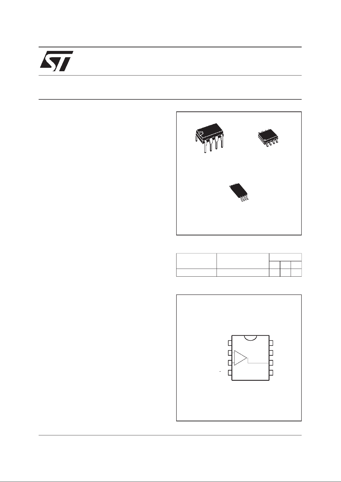
PIN CONNECTIONS (top view)
DESCRIPTION
The TS921is a RAILTO RAILsingle BiCMOS
operational amplifier optimized and fully specified
for 3V and 5V operation.
High outputcurrent allowslowload impedancesto
be driven.
The TS921exhibitsa verylownoise,lowdistortion,
low offsetand high ouput currentcapabilitymaking
this devicean excellent choicefor high quality,low
voltage or battery operated audio systems.
The device is stable for capacitive loads up to
500pF.
APPLICATIONS
.
headphoneamplifier
.
piezoelectricspeakerdriver
.
soundcards, multimedia systems
.
line driver, actuatordriver
.
servo amplifier
.
mobile phone and portablecommunication
sets
.
instrumentationwith low noise as a key factor
ORDER CODES
Part Number Temperature Range
Package
NDP
TS921I -40, +125
o
C •••
N
DIP8
(Plastic Package)
D
SO8
(Plastic Micropackage)
P
TSSOP8
(Thin Shrink Small Outline Package)
1/11
ABSOLUTEMAXIMUMRATINGS
Symbol Parameter Value Unit
V
CC
Supply Voltage - (note 1) 12 V
V
id
Differential Input Voltage - (note 2) ±1V
V
i
Input Voltage - (note 3) -0.3 to 14 V
T
oper
Operating Free Air Temperature Range -40 to +125
o
C
T
stg
Storage Temperature -65 to +150
o
C
T
j
Maximum Junction Temperature 150
o
C
Output Short Circuit Duration see note 4
o
C
Notes : 1. All voltage values, except differentialvoltage are with respect to networkground terminal.
2. Differential voltages are the non-inverting input terminal with respect to the inverting input terminal.
3. The magnitude of input and output voltages must never exceed V
CC
+
+0.3V.
4. Short-circuits can cause excessive heating.
OPERATINGCONDITIONS
Symbol Parameter Value Unit
V
CC
Supply Voltage 2.7to 12 V
V
icm
Common Mode Input Voltage Range V
CC
-
-0.2 to V
CC
+
+0.2 V
TS921
2/11
ELECTRICAL CHARACTERISTICS
V
CC
+
=3V,T
amb
=25oC (unless otherwisespecified)
Symbol Parameter Min. Typ. Max. Unit
V
io
InputOffset Voltage
T
min.
≤ T
amb
≤ T
max.
3
5
mV
DV
io
InputOffset Voltage Drift 2 µV/oC
I
io
InputOffset Current
V
out
= 1.5V 30
nA
I
ib
InputBias Current
V
out
= 1.5V 15 100
nA
V
OH
HighLevel Output Voltage RL= 600Ω
R
L
=32Ω
2.87
2.63
V
V
OL
Low Level Output Voltage RL= 600Ω
R
L
=32Ω 180
100 mV
A
vd
LargeSignal Voltage Gain (V
out
= 2Vpk-pk) RL= 600Ω
R
L
=32Ω
35
16
V/mV
I
CC
SupplyCurrent
no load, V
out=VCC/2
1 1.5
mA
GBP Gain Bandwidth Product
R
L
= 600Ω 4
MHz
CMR Common Mode Rejection Ratio 60 80 dB
SVR Supply Voltage Rejection Ratio
V
CC
= 2.7 to 3.3V 60 80
dB
I
o
Output Short Circuit Current 50 80 mA
SR Slew Rate 0.7 1.3 V/µs
∅m PhaseMargin at Unity Gain
R
L
= 600Ω,CL= 100pF 68
Degrees
G
m
Gain Margin
R
L
= 600Ω,CL= 100pF 12
dB
e
n
Equivalent Input Noise Voltage
f = 1kHz
9
nV
√Hz
THD Total Harmonic Distortion
V
out
= 2Vpk-pk, F = 1kHz, AV=1,RL= 600Ω 0.005
%
TS921
3/11
ELECTRICALCHARACTERISTICS
V
CC
+
=5V,T
amb
=25oC (unlessotherwise specified)
Symbol Parameter Min. Typ. Max. Unit
V
io
Input Offset Voltage
T
min.
≤ T
amb
≤ T
max.
3
5
mV
DV
io
Input Offset Voltage Drift 2 µV/oC
I
io
Input OffsetCurrent
V
out
= 1.5V 30
nA
I
ib
Input Bias Current
V
out
= 1.5V 15 100
nA
V
OH
High Level Output Voltage RL= 600Ω
R
L
=32Ω
4.85
4.4
V
V
OL
Low Level Output Voltage RL= 600Ω
R
L
=32Ω 300
120 mV
A
vd
Large Signal Voltage Gain (V
out
= 2Vpk-pk) RL= 600Ω
R
L
=32Ω
35
16
V/mV
I
CC
Supply Current
no load, V
out=VCC/2
1 1.5
mA
GBP Gain Bandwidth Product
R
L
= 600Ω 4
MHz
CMR Common Mode Rejection Ratio 60 80 dB
SVR Supply Voltage Rejection Ratio
V
CC
= 2.7 to 3.3V 60 80
dB
I
o
Output Short Circuit Current 50 80 mA
SR Slew Rate 0.7 1.3 V/µs
∅m Phase Margin at Unity Gain
R
L
= 600Ω,CL= 100pF 68
Degrees
G
m
Gain Margin
R
L
= 600Ω,CL= 100pF 12
dB
e
n
Equivalent Input Noise Voltage
f = 1kHz
9
nV
√Hz
THD Total Harmonic Distortion
V
out
= 2Vpk-pk, F = 1kHz, AV=1,RL= 600Ω 0.005
%
TS921
4/11

** StandardLinear Ics Macromodels,1996.
** CONNECTIONS:
* 1 INVERTINGINPUT
* 2 NON-INVERTINGINPUT
* 3 OUTPUT
* 4 POSITIVEPOWERSUPPLY
* 5 NEGATIVEPOWERSUPPLY
.SUBCKTTS92113245(analog)
*********************************************************
.MODEL MDTH D IS=1E-8 KF=2.664234E-16
CJO=10F
* INPUTSTAGE
CIP 2 5 1.000000E-12
CIN 1 5 1.000000E-12
EIP 10 5 2 51
EIN 16 5 1 5 1
RIP 10 118.125000E+00
RIN 15 16 8.125000E+00
RIS 1115 2.238465E+02
DIP 11 12 MDTH400E-12
DIN 15 14 MDTH400E-12
VOFP12 13 DC 153.5u
VOFN 13 14 DC0
IPOL 13 5 3.200000E-05
CPS 1115 1e-9
DINN 17 13 MDTH 400E-12
VIN 17 5 -0.100000e+00
DINR 15 18 MDTH 400E-12
VIP 4 18 0.400000E+00
FCP4 5VOFP 1.865000E+02
FCN 5 4 VOFN 1.865000E+02
FIBP2 5VOFP6.250000E-03
FIBN 5 1 VOFN 6.250000E-03
* GM1STAGE***************
FGM1P 119 5 VOFP1.1
FGM1N119 5 VOFN 1.1
RAP 119 4 2.6E+06
RAN119 5 2.6E+06
* GM2STAGE***************
G2P19 5 119 5 1.92E-02
G2N 19 5 1194 1.92E-02
R2P19 41E+07
R2N 19 5 1E+07
**************************
VINT1 500 0 5
GCONVP 500 501 119 4 19.38 !envoie ds VP,
I(VP)=(V119-V4)/2/Ut VP501 0 0
GCONVN 500 502 119 5 19.38 !envoie ds VN,
I(VN)=(V119-V5)/2/UtVN 502 0 0
*********orientation isink isource *******
VINT2 503 0 5
FCOPY503 504 VOUT 1
DCOPYP504 505 MDTH 400E-9
VCOPYP505 0 0
DCOPYN506 504 MDTH 400E-9
VCOPYN0 506 0
***************************
F2PP195poly(2)VCOPYPVP00000.5 !multiplie
I(vout)*I(VP)=Iout*(V119-V4)/2/Ut
F2PN 19 5 poly(2) VCOPYP VN 0 0 0 0 0.5
!multiplieI(vout)*I(VN)=Iout*(V119-V5)/2/Ut
F2NP 19 5 poly(2) VCOPYN VP 0 0 0 0 1.75
!multiplieI(vout)*I(VP)=Iout*(V119-V4)/2/Ut
F2NN 19 5 poly(2) VCOPYN VN 00001.75
!multiplieI(vout)*I(VN)=Iout*(V119-V5)/2/Ut
* COMPENSATION************
CC 19 11925p
* OUTPUT***********
DOPM19 22 MDTH 400E-12
DONM 21 19 MDTH 400E-12
HOPM22 28 VOUT6.250000E+02
VIPM28 45.000000E+01
HONM 21 27 VOUT6.250000E+02
VINM 5 27 5.000000E+01
VOUT3 23 0
ROUT 23 19 6
COUT 3 5 1.300000E-10
DOP 19 25 MDTH 400E-12
VOP4 25 1.052
DON 24 19 MDTH 400E-12
VON 24 5 1.052
.ENDS
.
RAILTO RAIL INPUT AND OUTPUT
.
LOW NOISE : 9nV√√
Hz
.
LOW DISTORTION
.
HIGHOUTPUTCURRENT : 80mA
(able to drive 32Ω loads)
.
HIGHSPEED: 4MHz, 1.3V/µs
.
OPERATING FROM 2.7V TO 12V
MACROMODEL
TS921
5/11

ELECTRICALCHARACTERISTICS
V
CC
+
= 3V, V
CC
-
= 0V,RL,CLconnectedto VCC/2, T
amb
=25oC
(unlessotherwisespecified)
Symbol Conditions Value Unit
V
io
0mV
A
vd
RL= 10kΩ 200 V/mV
I
CC
No load, per operator 1.2 mA
V
icm
-0.2 to 3.2 V
V
OH
RL= 10kΩ 2.95 V
V
OL
RL= 10kΩ 25 mV
I
sink
VO=3V 80 mA
I
source
VO=0V 80 mA
GBP R
L
= 600Ω 4 MHz
SR RL= 10k
Ω,
CL= 100pF 1.3 V/µs
∅mR
L
= 600Ω 68 Degrees
TS921
6/11

012345
-120
-100
-80
-60
-40
-20
0
20
40
60
80
100
Output Voltage (V)
Output Short-Circuit Current (mA)
Source
Sink
Vcc=0/5V
OUTPUT SHORT CIRCUITCURRENT vs
OUTPUT VOLTAGE
0 0,5 1 1,5 2 2,5 3
-100
-80
-60
-40
-20
0
20
40
60
80
100
Output Voltage (V)
Output Short-Circuit Current (mA)
Source
Sink
Vcc=0/3V
OUTPUT SHORT CIRCUIT CURRENT vs
OUTPUT VOLTAGE
024681012
0
1
2
3
Supply Voltage (V)
Supply Current (mA)
TOTALSUPPLYCURRENT vs SUPPLY
VOLTAGE
1E+02 1E+03 1E+04 1E+05 1E+06 1E+07 1E+08
-20
0
20
40
60
-60
0
60
120
180
Fre que ncy (Hz)
Gain (dB)
Phase (Deg)
phase
gain
Rl=10k
Cl=100pF
VOLTAGE GAIN AND PHASEvs FREQUENCY
0,01 0,1 1 10 100
0
5
10
15
20
25
30
Frequen cy (kHz)
Equivalent Input Noise (nV/sqrt(Hz))
Vcc=±1.5V
Rs=100ohms
EQUIVALENTINPUTNOISE VOLTAGEvs
FREQUENCY
TS921
7/11

0,01 0,1 1 10 100
0
0,005
0,01
0,015
0,02
Frequency (kHz)
THD+Noise (%)
RL=2k Vo=10Vpp
Vcc=±6V Av=1
THD + NOISE vs FREQUENCY
0,01 0,1 1 10 100
0
0,008
0,016
0,024
0,032
0,04
Frequency (kHz)
THD+Noise (%)
RL=32ohms Vo=4Vpp
Vcc= ±2.5V Av=1
THD+ NOISE vs FREQUENCY
0,01 0,1 1 10 100
0
0,1
0,2
0,3
0,4
0,5
0,6
0,7
Frequency (kHz)
THD+Noise(%)
RL=32ohms Vo=2Vpp
Vcc=±1.5V Av=10
THD + NOISE vs FREQUENCY
0 0,2 0,4 0,6 0,8 1 1,2
0,001
0,010
0,100
1,000
10,000
Vout (Vrms)
THD+Noise (%)
Rl=600ohms
f=1kHz
Vcc=0/3V
Av=-1
THD + NOISE vs OUTPUT VOLTAGE
0 0,2 0,4 0,6 0,8 1
0,01
0,1
1
10
Vout (Vrms)
THD+Noise (%)
RL=32ohms F=1kHz
Vcc=±1.5V Av= -1
THD + NOISE vs OUTPUT VOLTAGE
0 0,2 0,4 0,6 0,8 1 1,2
0,0001
0,001
0,01
0,1
1
10
Vout (Vrms)
THD+Noise (%)
RL=2kohms f=1kHz
Vcc=±1.5V Av= -1
THD + NOISE vs OUTPUT VOLTAGE
TS921
8/11

PACKAGE MECHANICALDATA
8 PINS- PLASTICPACKAGE
Dimensions
Millimeters Inches
Min. Typ. Max. Min. Typ. Max.
A 3.32 0.131
a1 0.51 0.020
B 1.15 1.65 0.045 0.065
b 0.356 0.55 0.014 0.022
b1 0.204 0.304 0.008 0.012
D 10.92 0.430
E 7.95 9.75 0.313 0.384
e 2.54 0.100
e3 7.62 0.300
e4 7.62 0.300
F 6.6 0260
i 5.08 0.200
L 3.18 3.81 0.125 0.150
Z 1.52 0.060
TS921
9/11

PACKAGE MECHANICALDATA
8 PINS- PLASTICMICROPACKAGE (SO)
Dimensions
Millimeters Inches
Min. Typ. Max. Min. Typ. Max.
A 1.75 0.069
a1 0.1 0.25 0.004 0.010
a2 1.65 0.065
a3 0.65 0.85 0.026 0.033
b 0.35 0.48 0.014 0.019
b1 0.19 0.25 0.007 0.010
C 0.25 0.5 0.010 0.020
c1 45
o
(typ.)
D 4.8 5.0 0.189 0.197
E 5.8 6.2 0.228 0.244
e 1.27 0.050
e3 3.81 0.150
F 3.8 4.0 0.150 0.157
L 0.4 1.27 0.016 0.050
M 0.6 0.024
S8
o
(max.)
TS921
10/11

Information furnished is believed to be accurate and reliable. However, STMicroelectronics assumes no responsibility for the
consequences of use of such information nor for any infringement of patents or other rights of third parties which may result from
its use. No license is granted by implication or otherwise under any patent or patent rights of STMicroelectronics. Specifications
mentioned in this publication are subject to change without notice. This publication supersedes and replaces all information
previously supplied.STMicroelectronics productsare not authorizedfor useas criticalcomponentsinlife support devicesor systems
without express written approval of STMicroelectronics.
The ST logo is a trademark of STMicroelectronics
1999 STMicroelectronics – Printed in Italy – All Rights Reserved
STMicroelectronics GROUP OF COMPANIES
Australia - Brazil - Canada - China - France - Germany - Italy - Japan - Korea - Malaysia - Malta - Mexico - Morocco
The Netherlands - Singapore -Spain - Sweden - Switzerland - Taiwan - Thailand - United Kingdom - U.S.A.
http://www.st.com
PACKAGE MECHANICALDATA
8 PINS- THIN SHRINK SMALL OUTLINE PACKAGE
Dim.
Millimeters Inches
Min. Typ. Max. Min. Typ. Max.
A 1.20 0.05
A1 0.05 0.15 0.01 0.006
A2 0.80 1.00 1.05 0.031 0.039 0.041
b 0.19 0.30 0.007 0.15
c 0.09 0.20 0.003 0.012
D 2.90 3.00 3.10 0.114 0.118 0.122
E 6.40 0.252
E1 4.30 4.40 4.50 0.169 0.173 0.177
e 0.65 0.025
k0
o
8
o
0
o
8
o
l 0.50 0.60 0.75 0.09 0.0236 0.030
TS921
11/11
 Loading...