

OPERATIONALAMPLIFIER (WITH STANDBY POSITION)
.
RAIL TO RAIL INPUTAND OUTPUT
VOLTAGERANGES
.
2SEPARATESTANDBY :REDUCED
CONSUMPTION(0.5µA) ANDHIGHIMPEDANCE OUTPUTS
.
SINGLE(ORDUAL) SUPPLY OPERATION
FROM 2.7VTO 16V
.
EXTREMELYLOW INPUTBIAS CURRENT:
1pA TYP
.
LOW INPUT OFFSETVOLTAGE : 5mVmax.
.
SPECIFIEDFOR 600Ω AND 150Ω LOADS
.
LOW SUPPLYCURRENT : 200µA/Ampli
.
SPICEMACROMODEL INCLUDEDIN THIS
SPECIFICATION
DESCRIPTION
The TS904is a RAILTORAILquad CMOSoperational amplifierdesignedto operatewithasingleor
dual supply voltage.
The input voltage range V
supplyrails V
The outputreaches :
• V
• V
-
+50mV V
CC
-
+350mV V
CC
CC
+
and V
CC
+
-50mV with RL=10kΩ
CC
+
-350mV with RL=600Ω
CC
This product offersa broad supply voltageoperating rangefrom 2.7Vto16V and a supplycurrentof
only 200µA/amp. (V
CC
= 3V)
Source and sink output current capability is typically 40mA (at V
= 3V), fixed by an internal
CC
limitationcircuit.
The TS904offers two separate STANDBYpins
• STANDBY1 acting on the n°2and
n°3operators
• STANDBY2 acting on the n°1and
n°4operators
Theyreducetheconsumptionofthecorresponding
operatorsandput theoutputsin a high impedance
state.
These two STANDBY pins should never stay not
connected.
STMicroelectronicsis offering a quad op-amp with
the same features : TS902.
includes the two
icm
-
.
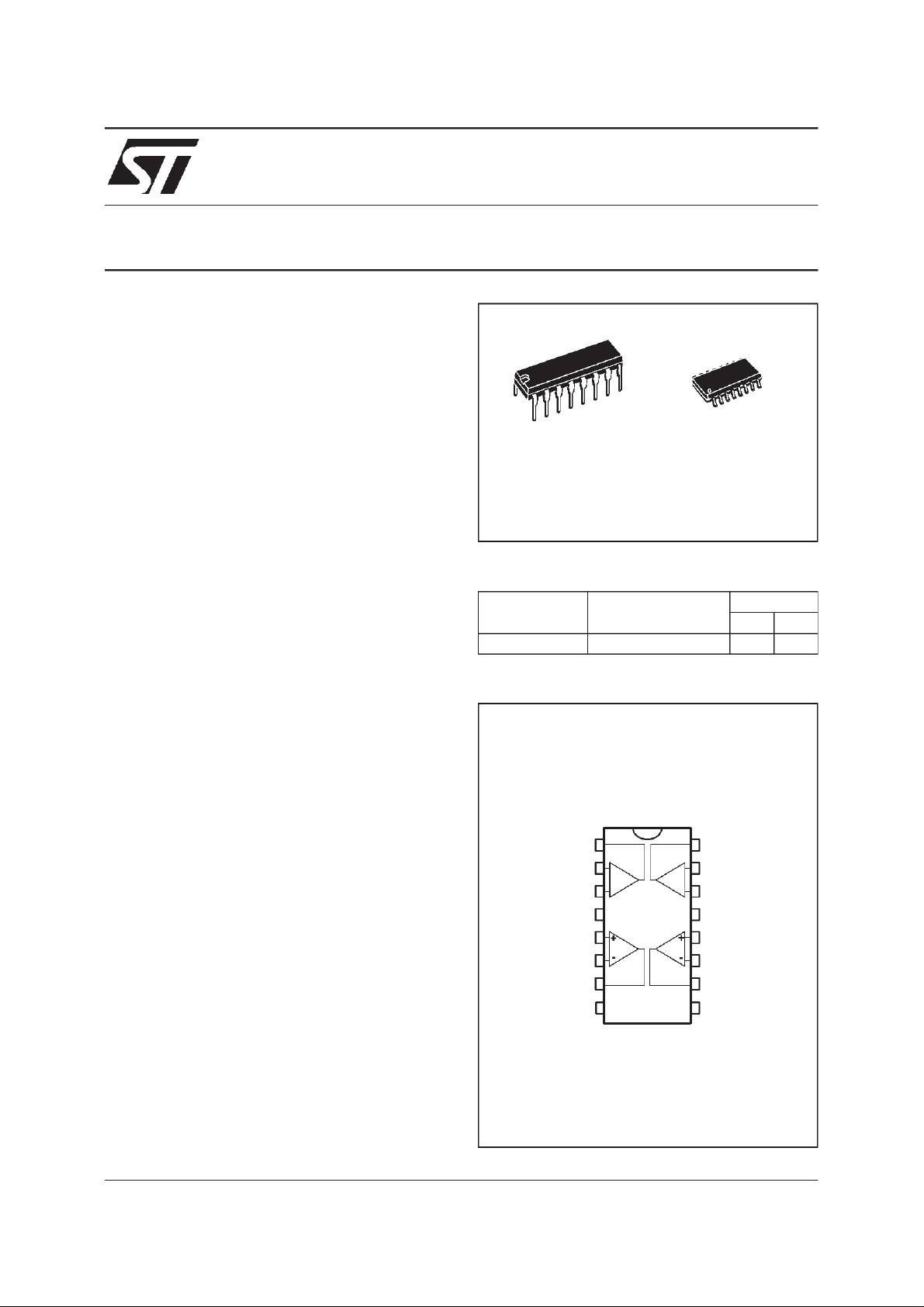
TS904
RAIL TO RAIL CMOS QUAD
N
DIP16
(Plastic Package)
(Plastic Micropackage)
ORDER CODES
Part Number Temperature Range
TS904I/AI -40, +125
PIN CONNECTIONS (top view)
Output 1
Inverting Inp ut 1
Non-inve rting inpu t1
Non-inve rting Input 2
Inverting Input 2
Output 2
Standby1
1
2
-
+
3
+
V
4
CC
5
6
7
8
D
SO16
Package
o
C ••
-
+
ND
Output 4
16
15
Inverting Inp ut 4
Non-inverting inpu t 4
14
-
V
13
CC
Non-inverting input3
12
Inverting input 3
11
Output 3
10
Standby 2
9
April 1999
1/12
TS904
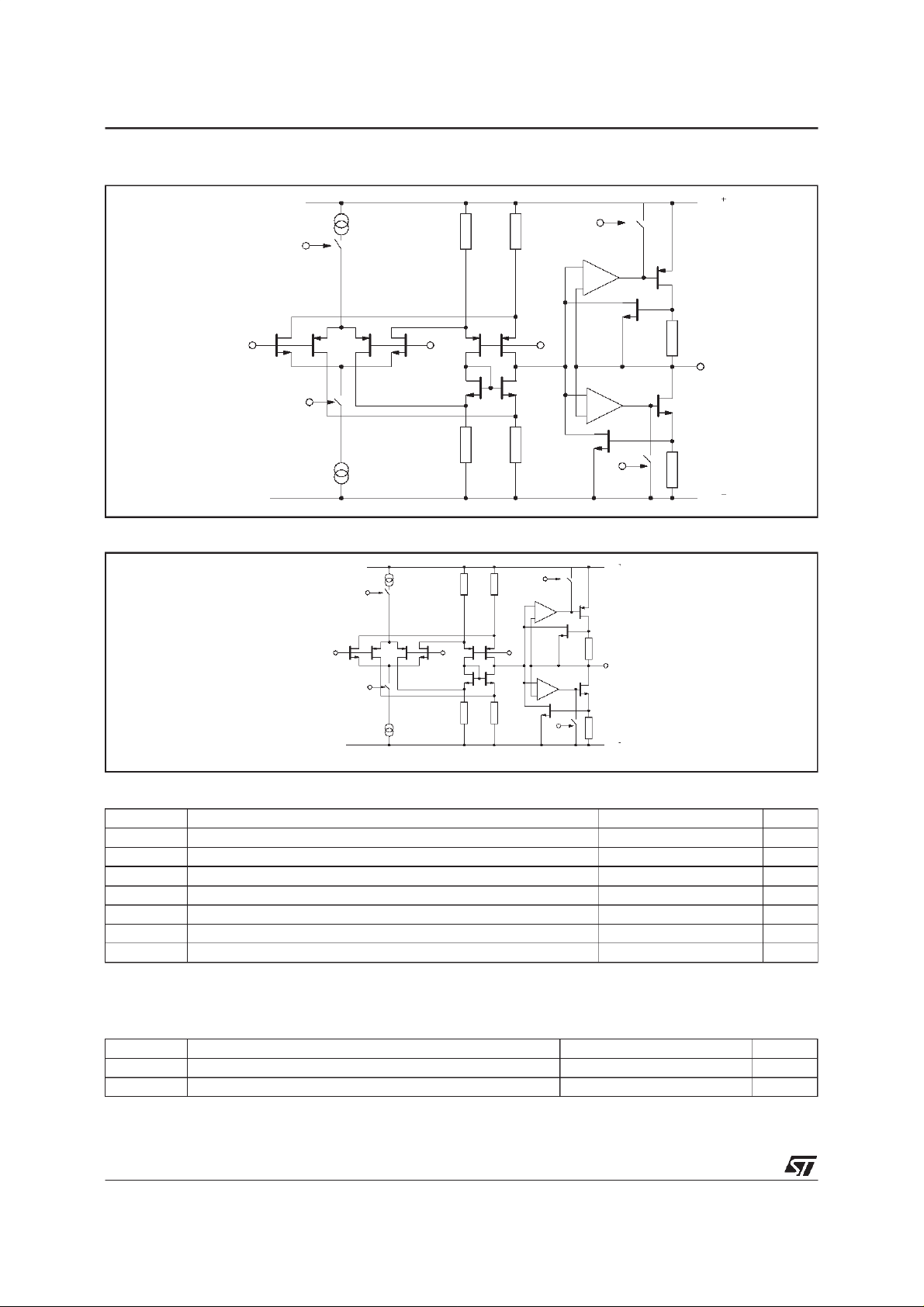
SCHEMATIC DIAGRAM (1/4TS904)
Standby
Non-inverting
Input
Standby
STANDBY POSITION
Sta ndb y
Inverting
Input
Interna l
Vref
Standby
Standby
Standby
V
CC
Output
V
CC
V
CC
Inte rnal
Non -invertin g
Inpu t
Standb y
Inve rting
Input
Vref
Outp ut
Standby
V
CC
ABSOLUTE MAXIMUMRATINGS
Symbol Parameter Value Unit
V
CC
V
id
V
I
in
I
o
T
oper
T
stg
Notes : 1. All voltage values, except differentialvoltage are with respect to network ground terminal.
Supply Voltage - (note 1) 18 V
Differential Input Voltage - (note 2) ±18 V
Input Voltage - (note 3) -0.3 to 18 V
i
Current on Inputs ±50 mA
Current on Outputs ±130 mA
Operating Free Air Temperature Range TS904I/AI -40 to +125
Storage Temperature -65 to +150
2. Differential voltages are the non-inverting inputterminal with respect to the inverting input terminal.
3. The magnitude of input and outputvoltages must never exceed V
CC
+
+0.3V.
OPERATING CONDITIONS
Symbol Parameter Value Unit
V
CC
V
icm
Supply Voltage 2.7 to 16 V
Common Mode Input VoltageRange V
CC
-
-0.2 to V
+
+0.2 V
CC
o
C
o
C
2/12
ELECTRICALCHARACTERISTICS
V
CC
+
=3V,V
-
=0V,RL,CLconnectedto VCC/2, pin 8 and pin 9 connectedto V
CC
CC
+
, T
amb
=25oC
(unlessotherwise specified)
Symbol
V
io
DV
io
I
io
I
ib
I
CC
InputOffset Voltage (Vic=Vo=VCC/2) TS904
≤ T
T
min.
amb
≤ T
max.
InputOffset Voltage Drift 5 µV/oC
InputOffset Current - (note1)
≤ T
T
min.
amb
≤ T
max.
InputBias Current - (note1)
≤ T
T
min.
amb
≤ T
max.
SupplyCurrent (per amplifier, A
≤ T
T
min.
amb
≤ T
max.
Parameter
= 1, no load)
VCL
TS904A
TS904
TS904A
CMR Common Mode Rejection Ratio
= 0 to 3V, Vo= 1.5V 40 70
V
ic
SVR SupplyVoltage RejectionRatio (V
A
V
V
LargeSignal VoltageGain (RL= 10kΩ,VO= 1.2V to 1.8V)
vd
High Level Output Voltage (Vid= 1V) RL= 10kΩ
OH
Low Level Output Voltage (Vid= -1V) RL= 10kΩ
OL
Output Short Circuit Current (Vid= ±1V) Source (Vo=V
I
o
≤ T
≤ T
≤ T
amb
amb
amb
≤ T
≤ T
≤ T
max.
max.
max.
T
min.
T
min.
T
min.
+
= 2.7 to 3.3V, VO=VCC/2) 40 70 dB
CC
= 600Ω
R
L
= 100Ω
R
L
RL= 10kΩ
= 600Ω
R
L
= 600Ω
R
L
= 100Ω
R
L
RL= 10kΩ
= 600Ω
R
L
Sink (V
CC
o=VCC
−
+
GBP GainBandwidth Product
= 100, RL= 10kΩ,CL= 100pF, f = 100kHz) 0.8
(A
VCL
+
SR
SR
Positive Slew Rate
=1,RL= 10kΩ,CL= 100pF, Vi=1.3V to 1.7V) 0.5
(A
VCL
-
NegativeSlew Rate
=1,RL= 10kΩ,CL= 100pF, Vi=1.3V to 1.7V) 0.4
(A
VCL
∅m Phase Margin 30 Degrees
e
Equivalent Input Noise Voltage (Rs= 100Ω, f = 1kHz) 30
n
V
O1/VO2
Note 1 : Maximum values including unavoidable inaccuracies of theindustrial test.
ChannelSeparation (f = 1kHz) 120 dB
Min. Typ. Max. Unit
1 100
1 150
200 300
3
10 V/mV
2
2.9
2.3
2.96
2.6
2
2.8
2.1
50
300
900
)
)
40
40
10
5
12
7
200
300
400
100
400
150
600
TS904
mV
pA
pA
µA
dB
V
mV
mA
MHz
V/µs
V/µs
nV
√Hz
3/12
TS904
ELECTRICALCHARACTERISTICS
+
=5V,V
V
CC
(unless otherwise specified)
Symbol Parameter Min. Typ. Max. Unit
V
io
DV
io
I
io
I
ib
I
CC
CMR Common Mode Rejection Ratio
SVR Supply Voltage Rejection Ratio (V
A
vd
V
OH
V
OL
I
o
GBP Gain Bandwidth Product
+
SR
-
SR
∅m Phase Margin 30 Degrees
Note 1 :Maximum values including unavoidable inaccuraciesof the industrial test.
-
=0V, RL,CLconnectedto VCC/2 ,pin8 and pin 9 connectedto V
CC
Input Offset Voltage (Vic=Vo=VCC/2) TS904
TS904A
≤ T
T
min.
amb
≤ T
max.
TS904
TS904A
CC
+
,T
amb
=25oC
10
5
12
7
Input Offset Voltage Drift 5 µV/oC
Input Offset Current - (note 1)
≤ T
T
min.
amb
≤ T
max.
Input Bias Current - (note1)
≤ T
≤ T
amb
amb
≤ T
≤ T
max.
max.
= 1, no load)
VCL
+
= 3 to 5V, VO=VCC/2) 50 80 dB
CC
T
min.
Supply Current (per amplifier, A
T
min.
= 1.5 to 3.5V, Vo= 2.5V 50 75
V
ic
Large Signal VoltageGain (RL= 10kΩ,VO= 1.5V to 3.5V)
≤ T
T
min.
amb
≤ T
max.
High Level Output Voltage (Vid= 1V) RL= 10kΩ
= 600Ω
R
L
= 100Ω
R
L
T
≤ T
min.
amb
≤ T
max.
RL= 10kΩ
= 600Ω
R
L
Low Level Output Voltage (Vid= -1V RL= 10kΩ
= 600Ω
R
L
= 100Ω
R
L
T
≤ T
amb
≤ T
max.
min.
Output Short Circuit Current (Vid= ±1V) Source (Vo=V
RL= 10kΩ
= 600Ω
R
L
Sink (V
CC
o=VCC
−
)
+
)
10
7
4.9
4.25
4.8
4.1
45
45
1 100
200
1 150
300
230 350
450
30 V/mV
4.95
4.65
3.7
50
350
100
500
1400
150
750
60
60
MHz
= 100, RL= 10kΩ,CL= 100pF, f =100kHz) 0.9
(A
VCL
Positive SlewRate (A
Negative Slew Rate (A
=1,RL= 10kΩ,CL= 100pF, Vi=1V to 4V) 0.8 V/µs
VCL
=1,RL= 10kΩ,CL= 100pF, Vi=1V to4V) 0.5 V/µs
VCL
mV
pA
pA
µA
dB
V
mV
mA
4/12

TS904
ELECTRICAL CHARACTERISTICS
+
=10V,V
V
CC
(unlessotherwisespecified)
Symbol Parameter Min. Typ. Max. Unit
V
Input Offset Voltage (Vic=Vo=VCC/2) TS904
io
DV
I
CMR Common Mode Rejection Ratio V
SVR Supply Voltage Rejection Ratio (V
A
V
V
GBP Gain Bandwidth Product
SR
SR
∅m Phase Margin 40 Degrees
THD Total Harmonic Distortion
V
O1/VO2
Note 1: Maximum valuesincluding unavoidable inaccuracies of theindustrial test.
Input Offset Voltage Drift 5 µV/oC
io
I
Input Offset Current -(note 1)
io
Input Bias Current - (note 1)
I
ib
Supply Current (per amplifier, A
CC
Large Signal Voltage Gain (RL= 10kΩ,VO= 2.5V to 7.5V)
vd
High Level Output Voltage(Vid= 1V) RL= 10kΩ
OH
Low Level Output Voltage(Vid= -1V) RL= 10kΩ
OL
Output Short Circuit Current (Vid= ±1V) Source (Vo=V
I
o
(A
+
Positive Slew Rate
(A
-
Negative Slew Rate
(A
e
Equivalent Input Noise Voltage (Rs= 100Ω, f = 1kHz) 30
n
(A
C
Input Capacitance 1.5 pF
in
Channel Separation (f = 1kHz) 120 dB
-
=0V,RL,CLconnectedto VCC/2, pin 8 and9 connectedto V
CC
TS904A
≤ T
max.
max.
max.
amb
≤ T
max.
VCL
= 1,no load)
+
CC
T
min.
≤ T
≤ T
≤ T
amb
amb
amb
≤ T
≤ T
≤ T
T
min.
T
min.
T
min.
TS904
TS904A
= 3 to 7V, Vo=5V
ic
= 0 to 10V, Vo=5V
V
ic
50 75
= 5 to 10V,VO=VCC/2) 50 80 dB
20
≤ T
T
min.
amb
≤ T
max.
15
9.85
= 600Ω
R
L
= 100Ω
R
≤ T
≤ T
amb
amb
≤ T
≤ T
max.
max.
T
min.
T
min.
= 100, RL= 10kΩ,CL= 100pF, f = 100kHz) 1.3
VCL
=1,RL= 10kΩ,CL= 100pF, Vi= 2.5V to 7.5V)
VCL
=1,RL= 10kΩ,CL= 100pF, Vi= 2.5V to 7.5V)
VCL
=1,RL= 10kΩ,CL= 100pF, VO= 4.75V to5.25V, f = 1kHz) 0.024
VCL
L
RL= 10kΩ
= 600Ω
R
L
= 600Ω
R
L
= 100Ω
R
L
RL= 10kΩ
= 600Ω
R
L
Sink (V
CC
o=VCC
−
)
+
)
9.2
9.8
9
45
45
+
,T
amb
=25oC
CC
10
5
12
7
1 100
200
1 150
300
400 600
700
70
60 V/mV
9.95
9.35
7.8
50
650
150
800
2300
150
900
60
60
1.3 V/µs
0.8 V/µs
mV
pA
pA
µA
dB
mV
mA
MHz
nV
√Hz
V
%
STANDBY MODE
V
CC
+
=10V,V
CC
-
=0V,T
=25oC (unlessotherwise specified)
amb
Symbol Parameter
V
in SBY/ON
V
in SBY/OFF
Pin 8/9 Threshold Voltagefor STANDBY ON 8.2 V
Pin 8/9 Threshold Voltagefor STANDBY OFF 8.5 V
Total Consumption
I
CC SBY
Standby 1ON - Standby 2 OFF
Standby 1OFF -Standby 2 ON
Standby 1and 2 ON
TS904I/AI
Min. Typ. Max.
800
800
2
Unit
µA
5/12

TS904
TYPICALCHARACTERISTICS (standby OFF = standby1 and2 OFF)
(standbyON = standby 1 and 2 ON)
Figure 1a : Supply Current (eachamplifier)
versus Supply Voltage
600
m
500
CC
400
T = 25 C
amb
A=1
VCL
V=V /2
o
CC
Sta ndby OFF
300
200
SUPPLY CURRENT, I ( A)
100
0481216
SUP PLYVOLTAGE, V (V)
CC
Figure 2 : Input Bias Current versus Temperature
100
V = 10V
CC
ib
INPUT BIAS CURRENT, I (pA)
V=5V
i
No loa d
Standby OFF
10
1
25 50 75 100 125
ambTEMPE RATURE , T ( C )
Figure1b :Supply Current(each amplifier)
versusSupply Voltage (in STANDBY
mode)
50
40
T = 25 C
amb
A=1
VCL
Sta ndby ON
µ
CC
30
20
10
SUPPLY CURRENT, I ( A)
0
48 1216
SUP P LY VOLTAGE, V (V)
CC
Figure3a : High Level Output Voltageversus
High Level Output Current
5
T=25C
amb
id
OH
4
V = 100mV
Standby OFF
3
2
1
OUTPUT VOLTAGE, V (V)
0
-70 -56 -42 -28 -1 4 0
OUTP UT CUR RENT, I (mA)
V = +5 V
CC
V = +3 V
CC
OH
Figure 3b : High Level OutputVoltage versus
HighLevel OutputCurrent
T=25C
amb
id
OUTP UT C UR RENT, I (m A)
V=+16V
CC
V=+10V
CC
OH
6/12
20
V = 100mV
StandbyOFF
16
OH
12
8
4
OUTPUT VOLTAGE, V (V)
0
-70 -56 -42 -28 -1 4 0
Figure4a : Low Level Output Voltageversus
Low Level OutputCurrent
5
T=25C
amb
id
V = +3 V
CC
V=+5V
CC
14 28 42 56 70
OUTP UT C URRENT, I (mA)
OL
OL
OUTPUT VOLTAGE, V (V)
4
3
2
1
0
V = 100mV
Sta ndbyOFF

TS904
Figure 4b : Low Level OutputVoltage versus
Low Level OutputCurrent
10
T=25C
amb
id
V = 16V
CC
V = 10V
CC
14 28 42 56 70
OUTP UT CURR ENT, I (m A)
OL
OL
OUTPUT VOLTAGE, V (V)
8
6
4
2
0
V = 100mV
Sta ndby OFF
Figure 5b : Gain andPhase vs Frequency
50
40
30
PHASE
T = 25 C
amb
20
V = 10V
GAIN (dB)
R=600
10
C = 100pF
A = 100
StandbyOFF
0
-
10
23
10
CC
Ω
L
L
VCL
10
FREQUENCY, f (Hz)
GAIN
Gain
Bandwidth
Product
4
10510
Phase
Margin
6
10
10
0
45
90
135
180
7
Figure5a : Gain and Phasevs Frequency
50
40
30
PHASE
GAIN
20
T=25 C
amb
V=10V
10
0
CC
R=10k
C = 100pF
A = 100
Standby OFF
L
L
VCL
Ω
Gain
Bandwidth
Product
GAIN (dB)
-10
23
10
10
4
10510
FREQUENCY, f (Hz)
Figure6a : Gain BandwidthProductversus
Supply Voltage
1800
1400
1000
PHASE (Degrees)
GAIN BANDW. PROD., GBP (kHz)
T=25 C
amb
R = 10k
C = 10 0pF
StandbyOFF
Ω
L
L
600
200
0481216
S UP P LY VOLTAGE, V (V)
10
Phase
Margin
6
CC
10
7
0
45
90
135
180
PHASE (Degrees)
Figure 6b : Gain bandwidth Product versus
SupplyVoltage
1800
T=25 C
amb
1400
R = 600
C = 100pF
Standby OFF
1000
600
200
GAIN BANDW. PROD., GBP (kHz)
0481216
Ω
L
L
S UP P LY VOLTAGE, V (V)
CC
Figure7a : Phase Marginversus Supply Voltage
60
T=25 C
amb
R=10k
50
φ
40
L
C = 100pF
Standby OFF
30
20
PHASE MARGIN, m (Degrees)
0481216
Ω
L
S UP P LY VOLTAGE, V (V)
CC
7/12

TS904
Figure7b : Phase Margin versusSupplyVoltage
60
T=25 C
amb
R = 600
50
φ
40
30
20
PHASE MARGIN, m (Degrees)
STANDBY APPLICATION
The TS904offers two separateSTANDBY pins :
.
STANDBY 1 (pin 8) acting on the n°2and n°3operators.
.
STANDBY 2 (pin 9) acting on the n°1and n°4operators.
When one of thesestandbyis activated (STANDBY ON) :
.
The supply currentof the correspondingoperators is considerablyreduced. The total consumptionof
the circuitis then dividedby 2 (oneSTANDBYON) or decreaseddown to 0.5µA(V
STANDBY ON) (ref. figure1b).
.
All the outputsof the corresponding operators are in high impedancestate. No outputcurrent can
then be sourced or sinked.
The standbypins 8 and 9 shouldnever stay unconnected.
.
The ”standbyOFF”state, isreached when the pins 8 or 9 voltage ishigher than V
.
The ”standbyON”state, is assured by the pins 8 or9 voltagelower than V
(see electricalcharacteristics)
L
C = 100pF
L
StandbyOFF
0481216
Ω
SUPPLY VOLTAGE, V (V)
CC
Figure8 : Input VoltageNoise versus Frequency
150
=10V
V
CC
=25 CT
amb
R
100
EQUIVALENT INPUT
VOLTAGE NOISE (nV/VHz)
50
0
10 100
FREQUENCY (Hz)
CC
in SBY/OFF
= 100
S
Standby OFF
1000
= 3V, two
in SBY/OFF
.
.
Ω
10000
8/12

MACROMODEL
TS904
.
RAIL TO RAIL INPUTAND OUTPUT
VOLTAGERANGES
.
2SEPARATESTANDBY :REDUCED
CONSUMPTION(2µA) ANDHIGH IMPEDANCE OUTPUTS
.
SINGLE(ORDUAL) SUPPLY OPERATION
FROM 2.7VTO 16V (±1.35Vto ±8V)
** Standard Linear Ics Macromodels, 1993.
** CONNECTIONS :
* 1 INVERTING INPUT
* 2 NON-INVERTING INPUT
* 3 OUTPUT
* 4 POSITIVEPOWER SUPPLY
* 5 NEGATIVEPOWER SUPPLY
* 6 STANDBY
.SUBCKT TS904 1 3 2 4 5 6 (analog)
**********************************************************
.MODEL MDTH D IS=1E-8 KF=6.563355E-14 CJO=10F
* INPUT STAGE
CIP 2 5 1.500000E-12
CIN 1 5 1.500000E-12
EIP 10 0 2 0 1
EIN 16 0 1 0 1
RIP 10 11 6.500000E+00
RIN 15 16 6.500000E+00
RIS 11 15 7.655100E+00
DIP 11 12 MDTH 400E-12
DIN 15 14 MDTH 400E-12
VOFP 1213 DC 0.000000E+00
VOFN 13 14 DC 0
FPOL 13 0 VSTB 1
CPS 11 15 3.82E-08
DINN 1713 MDTH 400E-12
VIN 17 5 -0.5000000e+00
DINR 1518 MDTH 400E-12
VIP 4 18 -0.5000000E+00
FCP 4 5 VOFP 8.6E+00
FCN 5 4VOFN 8.6E+00
ISTB0 5 4 900NA
* AMPLIFYING STAGE
FIP 0 19 VOFP 5.500000E+02
FIN 0 19 VOFN 5.500000E+02
RG1 19 120 5.087344E+05
GCOM1 120 5 POLY(1) 110 109 LEVEL=1 6.25E+11
RG2 121 19 5.087344E+05
GCOM2 121 4 POLY(1) 110 109 LEVEL=1 6.25E+11
CC 1929 2.200000E-08
HZTP 3029 VOFP 12.33E+02
HZTN 5 30 VOFN 12.33E+02
.
EXTREMELYLOWINPUT BIAS CURRENT :
1pA TYP
.
LOW INPUT OFFSETVOLTAGE: 5mV max.
.
SPECIFIEDFOR 600Ω AND 150Ω LOADS
.
LOW SUPPLYCURRENT :400µA/Ampli
(V
= 10V)
CC
DOPM 19 22 MDTH 400E-12
DONM 2119 MDTH 400E-12
HOPM 22 28 VOUT 3135
VIPM 28 4 150
HONM 2127 VOUT 3135
VINM 5 27 150
EOUT 26 23 195 1
VOUT 23 5 0
ROUT 26 103 65
COUT 1035 1.000000E-12
GCOM 103 3 POLY(1) 110 109 LEVEL=1 6.25E+11
* OUTPUT SWING
DOP 19 68 MDTH 400E-12
VOP 4 25 1.924
HSCP 68 25 VSCP1 1E8
DON 69 19 MDTH 400E-12
VON 24 5 2.4419107
HSCN 24 69 VSCN1 1.5E8
VSCTHP 60 61 0.1375
DSCP1 61 63 MDTH 400E-12
VSCP1 6364 0
ISCP 64 0 1.000000E-8
DSCP2 0 64 MDTH 400E-12
DSCN2 0 74 MDTH 400E-12
ISCN 74 0 1.000000E-8
VSCN1 73 74 0
DSCN1 7173 MDTH 400E-12
VSCTHN 7170 -0.75
ESCP 60 0 2 1 500
ESCN 70 0 2 1 -2000
* STAND BY
RMI1 4 111 1E+12
RMI2 5 111 1E+12
RSTBIN 6 0 1E+12
ESTBIN 106 0 6 0 1
ESTBREF 106 107 111 0 1
DSTB1 107 108 MDTH 400E-12
VSTB 108 109 0
ISTB 109 0 40U
RSTB 109110 1
DSTB2 0 110 MDTH 400E-12
.ENDS
9/12

TS904
ELECTRICALCHARACTERISTICS
+
= 10V, V
V
CC
(unlessotherwisespecified)
Symbol Conditions Value Unit
V
io
A
vd
I
CC
V
icm
V
OH
V
OL
I
sink
I
source
GBP R
SR RL= 10k
∅mR
I
CC STBY
-
= 0V,RL,CLconnectedto VCC/2, standby off,T
CC
amb
=25oC
0mV
RL= 10kΩ 40 V/mV
No load, per operator 400 µA
-0.2 to 10.2 V
RL= 10kΩ 9.95 V
RL= 10kΩ 50 mV
VO= 10V 60 mA
VO=0V 60 mA
= 10k
Ω,
L
= 10k
L
V
STBY
CL= 100pF 1.3 MHz
Ω,
CL= 100pF 1.3 V/µs
Ω,
CL= 100pF 40 Degrees
= 0V 800 nA
10/12

PACKAGE MECHANICAL DATA
16 PINS- PLASTICDIP
TS904
Dimensions
a1 0.51 0.020
B 0.77 1.65 0.030 0.065
b 0.5 0.020
b1 0.25 0.010
D 20 0.787
E 8.5 0.335
e 2.54 0.100
e3 17.78 0.700
F 7.1 0.280
i 5.1 0.201
L 3.3 0.130
Z 1.27 0.050
Min. Typ. Max. Min. Typ. Max.
Millimeters Inches
11/12

TS904
PACKAGE MECHANICAL DATA
16 PINS- PLASTICMICROPACKAGE(SO)
Dimensions
Min. Typ. Max. Min. Typ. Max.
Millimeters Inches
A 1.75 0.069
a1 0.1 0.2 0.004 0.008
a2 1.6 0.063
b 0.35 0.46 0.014 0.018
b1 0.19 0.25 0.007 0.010
C 0.5 0.020
c1 45
o
(typ.)
D 9.8 10 0.386 0.394
E 5.8 6.2 0.228 0.244
e 1.27 0.050
e3 8.89 0.350
F 3.8 4.0 0.150 0.157
G 4.6 5.3 0.181 0.209
L 0.5 1.27 0.020 0.050
M 0.62 0.024
S8
Information furnished is believed to be accurate and reliable. However, STMicroelectronics assumes no responsibility for the
consequences of use of such information nor for any infringement of patents or other rights of third parties which may result from
its use. No license is granted by implication or otherwise under any patent or patent rights of STMicroelectronics. Specifications
mentioned in this publication are subject to change without notice. This publ ication supersedes and replaces all infor mation
previously supplied.STMicroelectronics productsare not authorizedfor useas criticalcomponents in life supportdevices or systems
without express written approvalof STMicroelectronics.
The ST logo is a trademarkof STMicroelectronics
1999 STMicroelectronics– Printedin Italy – AllRights Reserved
STMicroelectronics GROUP OF COMPANIES
Australia - Brazil - Canada - China - France - Germany - Italy - Japan- Korea - Malaysia - Malta - Mexico- Morocco
The Netherlands - Singapore -Spain - Sweden - Switzerland -Taiwan - Thailand - United Kingdom - U.S.A.
http://www.st.com
o
(max.)
12/12
 Loading...