

Datasheet TS861IN, TS861ILT, TS861IDT, TS861ID, TS861AIN Datasheet (SGS Thomson Microelectronics)
...
1/11
.RAIL TO RAIL INPUTS
.PUSH PULL OUTPUT
.VERY LOW FALL & RISE TIME : 20ns
.VERY LOW PROPAGATIONDELAY : 500ns
.SUPPLY OPERATION FROM 2.7V TO 10V
.ULTRA LOW CURRENT CONSUMPTION :
6µA@VCC=3V
.ESD PROTECTION : 2KV (HBM) 200V (MM)
.AVAILABLE IN TINY SOT23-5 PACKAGE
DESCRIPTION
TheTS861 isaRAILTORAILsingleBiCMOScomparator optimized and fully specified for 2.7V, 5V
and 10V operations.
The TS861 exhibits an excellent speed to power
consumptionratio, making this device an excellent
choice for battery operated systems.
The TS861 has a push-pull output allowing direct
connectionto microcontroller without pull-upresistors.
APPLICATIONS
.Cordless telephones and portable communica-
tion equipments
.Metering systems
.Portable computers
.Battery powered alarms
PIN CONNECTIONS (top view)
ORDER CODES
Part
Number
Temperature
Range
Package SOT23-5
Marking
ND L
TS861I
-40
o
C, +85oC
••• K501
TS861AI ••• K502
Example : TS861IN
L
SOT23-5
(Tiny Package)
SINGLE BiCMOS RAIL TO RAIL
3V µPOWER COMPARATOR
TS861
March 2000
1
2
3
45
6
7
8
-
+
N.C.
Inverting input
Non-inverting input
V
CC
Output
-
V
CC
+
N.C.
N.C.
DIP8-SO8
1
2
3
4
5
Inverting inp ut
Non-inve rting inp ut
Outpu t
V
CC
-
V
CC
+
SOT23-5
N
DIP8
(Plastic Package)
D
SO8
(Plastic Micropackage)

TS861
2/11
Notes : 1. All voltages values, except differential voltage, are with respect to networkground terminal.
2. Differential voltages are non-inverting inputterminal with respect to the inverting inputterminal.
3. The magnitude of inputand output voltages must never exceedVCC+0.3V.
4. Tj= 150oC, T
amb
=25oC with R
thja
= 250oC/W for SOT23-5package
R
thja
= 175oC/W for SO8package
R
thja
= 100oC/W for DIP8package
ABSOLUTE MAXIMUM RATINGS
Symbol Parameter Value Unit
V
cc
Supply Voltage- (note 1) 12 V
V
id
Differential Input Voltage - (note 2)
±12
V
V
i
Input Voltage- (note 3) -0.3 to +12 V
T
oper
Operating Free Air TemperatureRange -40 to +85
o
C
T
stg
Storage Temperature -65 to +150
o
C
T
j
Maximum Junction Temperature 150
o
C
P
d
Maximum power dissipation - (note 4) SOT23-5
SO8
DIP8
500
715
1200
mW
OPERATING CONDITIONS
Symbol Parameter Value Unit
V
cc
Supply Voltage 2.7 to 10 V
V
icm
Common Mode Input Voltage Range (V
CC
-
) -0.3 to (V
CC
+
) +0.3 V

TS861
3/11
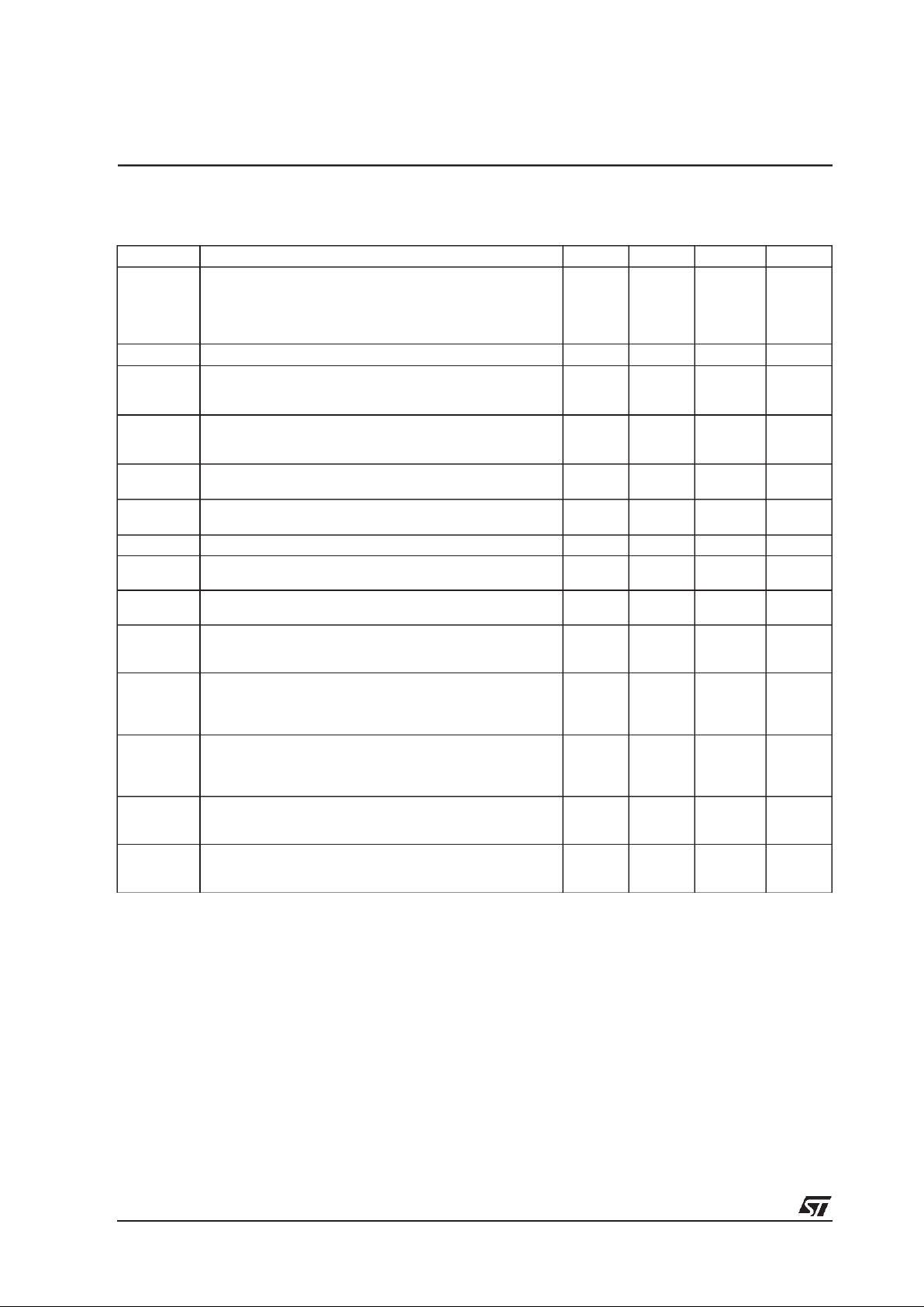
ELECTRICAL CHARACTERISTICS
V
CC
+
= 2.7V, T
amb
= 25oC (unless otherwise specified)
Symbol Parameter Min. Typ. Max. Unit
V
io
Input Offset Voltage (Full common mode range)
TS861A T
amb
= +25oC
T
min.
≤ T
amb
≤ T
max
.
TS861 T
amb
= +25oC
T
min.
≤ T
amb
≤ T
max
.
7
10
15
18
mV
DV
io
Input Offset Voltage Drift 6
µV/
o
C
I
io
Input Offset Current
T
amb
= +25oC
T
min.
≤ T
amb
≤ T
max
.
1
300
pA
I
ib
Input BiasCurrent
T
amb
= +25oC
T
min.
≤ T
amb
≤ T
max
.
1
600
pA
Voh High Level Output Voltage - I
source
= 2.5mA
T
min.
≤ T
amb
≤ T
max
.
2.35
2.15
2.45 V
Vol Low Level Output Voltage -I
sink
= 2.5mA
T
min.
≤ T
amb
≤ T
max
.
0.2 0.35
0.45
V
A
vd
Large Signal Voltage Gain (design evaluation) 240 dB
CMR Common-mode Rejection Ratio
0<V
icm
< 2.7V 65
dB
SVR Supply VoltageRejection Ratio
2.7 <V
CC
< 10V 80
dB
I
CC
Supply Current
No load, output low
No load, output high
6
8
12
14
µA
tplh Response Time Low to High
V
ic
= 1.35V, f = 10kHz, CL= 50pF
Overdrive = 10mV
Overdrive = 100mV
1.5
0.6
µs
tphl Response Time High toLow
V
ic
= 1.35V, f = 10kHz, CL= 50pF
Overdrive = 10mV
Overdrive = 100mV
1.5
0.5
µs
tf Fall Time
f =10kHz, C
L
= 50pF
Overdrive =100mV
20
ns
tr Rise Time
f =10kHz, C
L
= 50pF
Overdrive =100mV
20
ns
TS861
4/11
ELECTRICAL CHARACTERISTICS
V
CC
+
= 5V, T
amb
= 25oC (unless otherwise specified)
Symbol Parameter Min. Typ. Max. Unit
V
io
Input Offset Voltage (Full common mode range)
TS861A T
amb
= +25oC
T
min.
≤ T
amb
≤ T
max
.
TS861 T
amb
= +25oC
T
min.
≤ T
amb
≤ T
max
.
7
10
15
18
mV
DV
io
Input Offset Voltage Drift 6
µV/
o
C
I
io
Input Offset Current
T
amb
= +25oC
T
min.
≤ T
amb
≤ T
max
.
1
300
pA
I
ib
Input BiasCurrent
T
amb
= +25oC
T
min.
≤ T
amb
≤ T
max
.
1
600
pA
Voh High Level Output Voltage - I
source
= 5mA
T
min.
≤ T
amb
≤ T
max
.
4.6
4.45
4.8 V
Vol Low Level Output Voltage -I
sink
= 5mA
T
min.
≤ T
amb
≤ T
max
.
0.2 0.4
0.55
V
A
vd
Large SignalVoltage Gain (design evaluation) 240 dB
CMR Common-mode Rejection Ratio
0<V
icm
<5V 70
dB
SVR Supply VoltageRejection Ratio
2.7 < V
CC
< 10V 80
dB
I
CC
Supply Current
No load, output low
No load, output high
6
8
12
14
µA
tplh Response Time Low to High
V
ic
= 2.5V, f = 10kHz,CL= 50pF
Overdrive =10mV
Overdrive =100mV
2
0.5
µs
tphl Response Time High to Low
V
ic
= 2.5V, f = 10kHz,CL= 50pF
Overdrive =10mV
Overdrive =100mV
2
0.4
µs
tf Fall Time
f = 10kHz, C
L
= 50pF
Overdrive = 100mV
20
ns
tr Rise Time
f = 10kHz, C
L
= 50pF
Overdrive = 100mV
20
ns

TS861
5/11
ELECTRICAL CHARACTERISTICS
V
CC
+
= 10V, T
amb
= 25oC (unless otherwise specified)
Symbol Parameter Min. Typ. Max. Unit
V
io
Input Offset Voltage (V
icm=VCC/2
)
TS861 T
amb
= +25oC
T
min.
≤ T
amb
≤ T
max
.
15
18
mV
DV
io
Input Offset Voltage Drift 6
µV/
o
C
I
io
Input Offset Current
T
amb
= +25oC
T
min.
≤ T
amb
≤ T
max
.
1
300
pA
I
ib
Input BiasCurrent
T
amb
= +25oC
T
min.
≤ T
amb
≤ T
max
.
1
600
pA
Voh High Level Output Voltage - I
source
= 5mA
T
min.
≤ T
amb
≤ T
max
.
9.6
9.45
9.8 V
Vol Low Level Output Voltage -I
sink
= 5mA
T
min.
≤ T
amb
≤ T
max
.
0.2 0.4
0.55
V
A
vd
Large SignalVoltage Gain (design evaluation) 240 dB
CMR Common-mode Rejection Ratio
0<V
icm
< 10V 75
dB
SVR Supply VoltageRejection Ratio
2.7 < V
CC
< 10V 80
dB
I
CC
Supply Current
No load, output low
No load, output high
7
10
14
16
µA
tplh Response Time Low to High
V
ic
= 5V, f = 10kHz,CL= 50pF
Overdrive =10mV
Overdrive =100mV
3
0.5
µs
tphl Response Time High to Low
V
ic
= 5V, f = 10kHz,CL= 50pF
Overdrive =10mV
Overdrive =100mV
2.6
0.4
µs
tf Fall Time
f = 10kHz, C
L
= 50pF
Overdrive = 100mV
20
ns
tr Rise Time
f = 10kHz, C
L
= 50pF
Overdrive = 100mV
20
ns

TS861
6/11
Input Offset Voltage (Vio) vs Common Mode
Voltage (V
icm
)
Input Offset Voltage (Vio) vs Temperature
@VCC=5V
Input Offset Voltage (Vio) vs Supply
Voltage (VCC)
Supply Current (ICC) vs Supply Voltage (VCC)
Output Low Voltage (Vol) vs Sinking Current
(I
sink
)@VCC=5V
Output High Voltage (Voh) vs Sourcing
Current (I
source
)@VCC=5V

TS861
7/11
Supply Current (ICC) vs Temperature :
Output Low
Supply Current (ICC) vs Temperature :
Output High
Response Time @ VCC= 5V Response Time @ VCC=5V
Response Time @ VCC= 5V Response Time @ VCC=5V

TS861
8/11
Response Time @ VCC= 5V Response Time @ VCC=5V
Response Time @ VCC= 5V Response Time @ VCC=5V

TS861
9/11
PACKAGE MECHANICAL DATA
8 PINS - PLASTICPACKAGE
Dim.
Millimeters Inches
Min. Typ. Max. Min. Typ. Max.
A 3.32 0.131
a1 0.51 0.020
B 1.15 1.65 0.045 0.065
b 0.356 0.55 0.014 0.022
b1 0.204 0.304 0.008 0.012
D 10.92 0.430
E 7.95 9.75 0.313 0.384
e 2.54 0.100
e3 7.62 0.300
e4 7.62 0.300
F 6.6 0260
i 5.08 0.200
L 3.18 3.81 0.125 0.150
Z 1.52 0.060

TS861
10/11
PACKAGE MECHANICAL DATA
8 PINS - PLASTICMICROPACKAGE (SO)
Dim.
Millimeters Inches
Min. Typ. Max. Min. Typ. Max.
A 1.75 0.069
a1 0.1 0.25 0.004 0.010
a2 1.65 0.065
a3 0.65 0.85 0.026 0.033
b 0.35 0.48 0.014 0.019
b1 0.19 0.25 0.007 0.010
C 0.25 0.5 0.010 0.020
c1 45
o
(typ.)
D 4.8 5.0 0.189 0.197
E 5.8 6.2 0.228 0.244
e 1.27 0.050
e3 3.81 0.150
F 3.8 4.0 0.150 0.157
L 0.4 1.27 0.016 0.050
M 0.6 0.024
S8
o
(max.)

TS861
11/11
L
C
E1
A2
A
A1
b
E
D
PACKAGE MECHANICAL DATA
5 PINS - TINY PACKAGE (SOT23)
Dim.
Millimeters Inches
Min. Max. Min. Max.
A 0.90 1.45 0.034 0.057
A1 0 0.15 0.006
A2 0.90 1.30 0.034 0.051
b 0.35 0.50 0.013 0.020
C 0.09 0.20 0.003 0.008
D 2.80 3.00 0.110 0.118
E 2.60 3.00 0.102 0.118
E1 1.50 1.75 0.059 0.069
L 0.10 0.60 0.003 0.024
Informationfurnished is believedto be accurateand reliable.However, STMicroelectronicsassumes no responsibility forthe consequences ofuse of such information nor forany infringementof patentsor otherrightsof third parties which mayresultfrom its use.
No licenseis granted by implication orotherwise under any patentor patent rightsof STMicroelectronics. Specifications mentioned
in this publication are subject to change without notice. This publication supersedes and replaces all information previously supplied. STMicroelectronics products arenot authorizedfor use as critical components in life supportdevices orsystems without express written approval of STMicroelectronics.
The ST logo is a trademarkof STMicroelectronics
2000 STMicroelectronics– Printed in Italy – All Rights Reserved
STMicroelectronics GROUP OF COMPANIES
Australia -Brazil - China - Finland - France - Germany - Hong Kong- India - Italy - Japan - Malaysia - Malta- Morocco
Singapore - Spain - Sweden - Switzerland - United Kingdom
http://www.st.com
 Loading...