


MICROPOWER VOLTAGE SUPERVISOR
.
ULTRA LOWPOWERCONSUMPTION :
12µAmax.@ V
.
PRECISIONRESETTHRESHOLD(guaranteed overTemperature)
.
4.50Vtyp.THRESHOLDVOLTAGE(TS836-4)
.
GUARANTEEDRESETOPERATIONFOR
DOWN TO1V
V
CC
.
OPENDRAIN OUTPUTCOMPARATOR
WITH V
4V
.
FASTRESPONSE TIME : 20µs FORA10mV
OVERDRIVE
.
100mV INTERNALHYSTERESIS
= 450mVtyp. @ Iol= 8mA& VCC=
ol
CC
=5V
TS836
RESET ACTIVEHIGH
D
SO8
(PlasticMicropackage)
Z
TO92
(Plastic Package)
DESCRIPTION
The TS836ultra lowpowerintegratedcircuitincorporates ahigh stabilityband gap voltagereference
and a comparatorwith open drain output.
The thresholdvoltageisset at 4.5Vfor TS836-4by
internal thermally matched resistances.
The comparator exhibits a 20µs response (with
10mV overdrive) and has an open drain output
activewhen inputvoltageishigher thanthethreshold.
An internalhysteresisof100mVincreasesthecomparator’s noise margin and prevents false reset
operation.
APPLICATIONS
.
Power-onreset generatorfor microcontroler
.
Power failuredetector
ORDER CODES
Part Number Temperature Range
TS836-4I -40, +85
PIN CONNECTIONS
TO92
(topview)
12
OUT
3
IN
GND
o
Package
DZ
C • ù
SO8
NC NC NC
8765
1234
OUT IN NC
NC
GND
September 1998
1/8

TS836
ABSOLUTEMAXIMUMRATINGS
Symbol Parameter Value Unit
V
CC
V
out
I
out
Pd Power Dissipation 200 mW
T
oper
T
stg
Note: 1. All voltages values, except differential voltage are withrespect to network ground terminal.
OPERATINGCONDITIONS
Symbol Parameter Value Unit
V
CC
TS836-4
ELECTRICAL CHARACTERISTICS T
Symbol Parameter Min. Typ. Max. Unit
V
thi
V
thd
V
hys
I
CC
V
OL
I
OH
tphl Response Time High to Low
Supply Voltage - note 1 7 V
Output Voltage -0.3 to V
+
0.3 V
CC
Output Current 20 mA
Operating Free Air Temperature Range -40 to +85
Storage Temperature -65 to +150
Supply Voltage 1 to 5.5 V
=25oC (unless otherwisespecified)
amb
Threshold Voltage - VCCIncreasing
≤ T
T
min.
amb
≤ T
max.
Threshold Voltage - VCCDecreasing
≤ T
T
min.
amb
≤ T
max.
4.17 4.5 4.66 V
4.17 4.4 4.66 V
Hysteresis Voltage 50 100 200 mV
Current Consumption VCC=5V 12 µA
Low Level OutputVoltage VCC=4V
= 8mA, T
I
OL
min.
≤ T
amb
≤ T
max.
Output Off-state Leakage VCC=5V
≤ T
T
min.
amb
≤ T
max.
450 800
1000
2 100
1000
20 µs
RL= 10kΩ,CL= 15pF, VCC=V
thd
-10mV
o
o
mV
nA
C
C
2/8
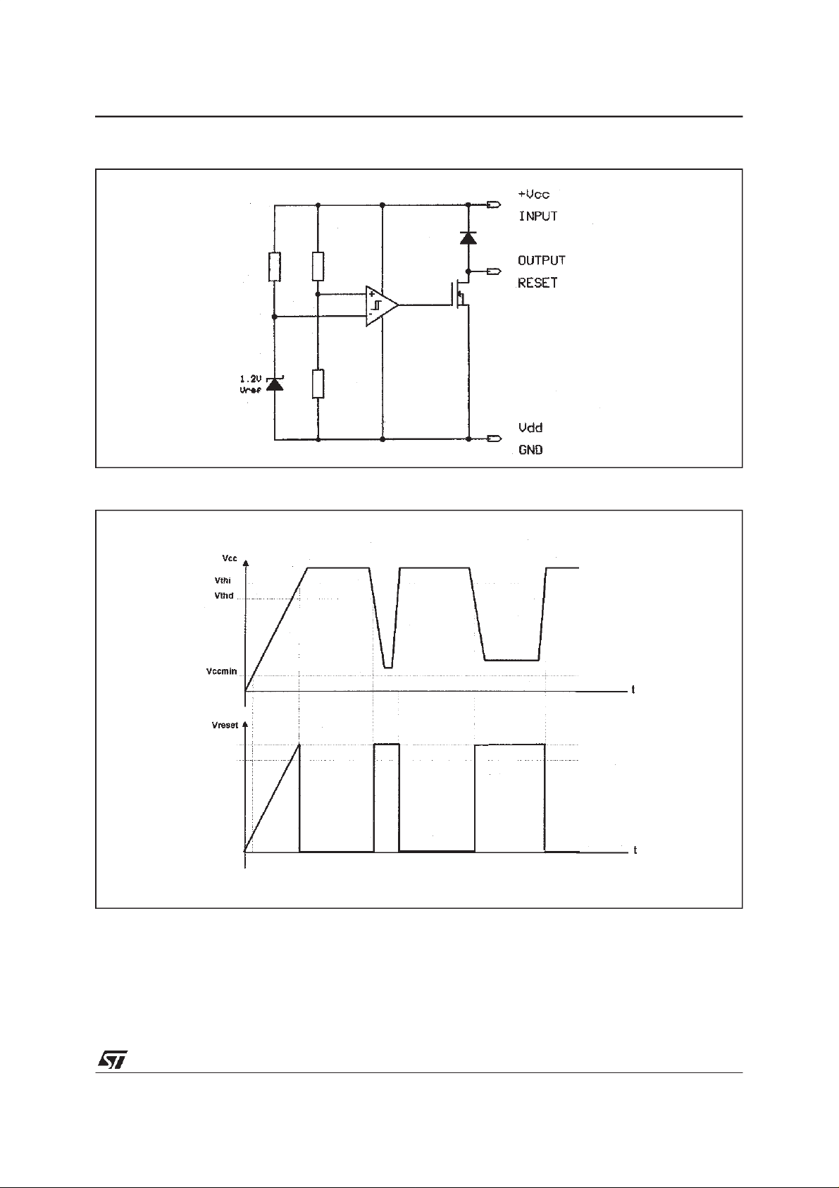
EQUIVALENTSCHEMATIC DIAGRAM
TIMING DIAGRAM
TS836
3/8

TS836
Vth vs Temperaturewhile VCCincreasing
Vthi (Volts)
4,56
max
4,52
4,48
4,44
4,4
-50 -40 -30 -20 -10 0 10 20 30 40 50 60 70 80 90 100 110 120
Vthi
Vth i
min
TS836-4
Temperature (°C)
Hysteresisvs Temperature
Hysteresis(mV)
160
TS836-4
140
120
100
80
60
-50 -40 -30 -20 -10 0 10 20 30 40 50 60 70 80 90 100 110 120
Temperature(°C)
Vth vs Temperature while VCCdecreasing
Vthd (Volts)
4,44
x
4,42
4,4
4,38
4,36
4,34
4,32
-50 -40 -30 -20 -10 0 10 20 30 40 50 60 70 80 90 100 110 120
Vth d
ma
Vth d
n
i
m
Temperature (°C)
TS836-4
ICCvs Temperature
Icc (µA)
9,6
9,4
9,2
9
8,8
8,6
8,4
8,2
-50 -40 -30 -2 0 -10 0 10 20 30 40 50 60 70 80 90 100 110 120
x
ma
c
c
I
min
c
c
I
TS836-4
Temperature (°C)
Reset Output Voltage vs Input Voltage
Outputvoltage (V)
5
4
3
2
1
0
4,3 4,4 4,5 4,6
Input voltage(V)
4/8
TS836-4
RL=10Kohms
T=25°C
Voltage Output Low vs Sink Current
Vol (Volts)
1
0,8
0,6
0,4
0,2
0
0 2 4 6 8 10 12 14 16 18 20
TS836-4
T=25°C
Isink (mA)

TS836
Reset Output Voltage vs Input Voltage
TS836-4
RL=10Kohms
T=25°C
Input signal
2V/div
0.5ms/div
Reset output
2V/div
0.5ms/div
5V
0V
5V
0V
SupplyFalling down : Extended Reset Delay
Timewith an Additional Capacitor
Input sig nal
0.5V/div
0.1 ms/div
Reset output
2V/div
0.1 ms/div
5V
3.5V
3.5V
0V
TS836-4
RL=10 Kohms
CL=10 nF
T=25°C
SupplyFalling down : Reset Delay Time
Input signal
0.5V/div
10 µs/div
Reset output
2V/div
10 µs/div
5V
3.5V
3.5V
0V
TS836-4
RL=10Kohms
T=25°C
SupplyRising up : Output Delay Time
5V
Input signal
0.5V/div
0.5 µs/div
Reset output
2V/div
0.5 µs/div
3.5V
5V
0V
TS836-4
RL=10 Kohms
T=25°C
Reset Output Voltage vs Input Voltage
(example)
Input signal
2 V/d iv
0.5 ms/div
Reset output
2V/div
0.5 ms/div
6V
4V
RL=10 Kohms
6V
0V
TS836-4
T=25°C
Reset Output Voltagevs InputVoltage
(example)
Input signal
2 V/div
0.5 ms/div
Reset output
2V/div
0.5 ms/div
5V
3V
5V
0V
TS836-4
RL=10 Kohms
T=25°C
5/8

TS836
Basic Configuration
Resistor
Vcc
Input
Voltage
TS836
Load
Output
Voltage
Reset
Configurationwith an additional Capacitive
Load
Load Resistor
Vcc Reset
Input
Voltage
TS836
Capacitive
Load
Output
Voltage
6/8

PACKAGE MECHANICAL DATA
8 PINS- PLASTICMICROPACKAGE (SO)
TS836
Dim.
A 1.75 0.069
a1 0.1 0.25 0.004 0.010
a2 1.65 0.065
a3 0.65 0.85 0.026 0.033
b 0.35 0.48 0.014 0.019
b1 0.19 0.25 0.007 0.010
C 0.25 0.5 0.010 0.020
c1 45
D 4.8 5.0 0.189 0.197
E 5.8 6.2 0.228 0.244
e 1.27 0.050
e3 3.81 0.150
F 3.8 4.0 0.150 0.157
L 0.4 1.27 0.016 0.050
M 0.6 0.024
S8
Min. Typ. Max. Min. Typ. Max.
Millimeters Inches
o
(typ.)
o
(max.)
7/8

TS836
PACKAGE MECHANICAL DATA
3 PINS- PLASTICPACKAGE TO92
Dim.
Min. Typ. Max. Min. Typ. Max.
Millimeters Inches
L 1.27 0.05
B 3.2 3.7 4.2 0.126 0.1457 0.1654
O1 4.45 5.00 5.2 0.1752 0.1969 0.2047
C 4.58 5.03 5.33 0.1803 0.198 0.2098
K 12.7 0.5
O2 0.407 0.5 0.508 0.016 0.0197 0.02
a 0.35 0.0138
Information furnished is believed to be accurate and reliable. However, STMicroelectronics assumes no responsibility for the
consequences of use of such information nor for any infringement of patents or other rights of third parties which may result from
its use. No license is granted by implication or otherwise under any patent or patent rights of STMicroelectronics. Specifications
mentioned in this publication are subject to change without notice. This publication supersedes and replaces all information
previously supplied.STMicroelectronics productsarenot authorized for useas critical components inlife supportdevices or systems
without express written approvalof STMicroelectronics.
The ST logo is atrademark of STMicroelectronics
8/8
1998 STMicroelectronics – Printed in Italy –All Rights Reserved
STMicroelectronics GROUP OF COMPANIES
Australia - Brazil - Canada - China - France - Germany - Italy - Japan - Korea - Malaysia -Malta -Mexico - Morocco
The Netherlands - Singapore - Spain - Sweden - Switzerland- Taiwan - Thailand - United Kingdom - U.S.A.
 Loading...