

Datasheet TYN808, TYN1008, TYN608, TS820-700H, TS820-700B Datasheet (SGS Thomson Microelectronics)
...
1/9
®
TN8, TS8 and TYNx08 Series
SENSITIVE & STANDARD 8A SCRs
April 2002 - Ed: 4A
MAIN FEATURES:
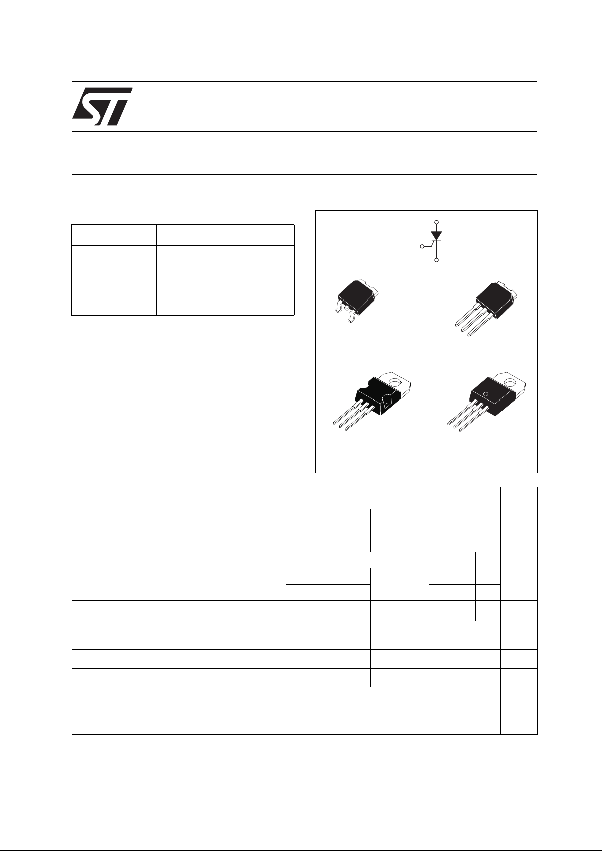
DESCRIPTION
Available either in sensitive (TS8) or standard
(TN8 / TYN) gate triggering levels, the 8A SCR
series is suitable to fit all modes of control, found
in applications such as overvoltage crowbar
protection, motor control circuits in power tools
and kitchen aids, inrush current limiting circuits,
capacitive discharge ignition and voltage
regulation circuits...
Available in through-hole or surface-mount
packages, they provide an optimized performance
in a limited space area.
Symbol Value Unit
I
T(RMS)
8A
V
DRM/VRRM
600 to 1000 V
I
GT
0.2 to 15 mA
ABSOLUTE RATINGS (lim iting values)
Symbol Parameter Value Unit
I
T(RMS)
RMS on-state current (180° conduction angle)
Tc = 110°C 8
A
IT
(AV)
Average on-state current (180° conduction angle)
Tc = 110°C 5
A
TS8/TN8 TYN
I
TSM
Non repetitive surge peak on-state
current
tp = 8.3 ms
Tj = 25°C
73 100
A
tp = 10 ms 70 95
I
²
tI
²
t Value for fusing
tp = 10 ms Tj = 25°C 24.5 45
A
2
S
dI/dt
Critical rate of rise of on-state current
I
G
= 2 x IGT , tr ≤ 100 ns
F = 60 Hz Tj = 125°C 50 A/µs
I
GM
Peak gate current tp = 20 µs Tj = 125°C 4 A
P
G(AV)
Average gate power dissipation Tj = 125°C 1 W
T
stg
Tj
Storage junction temperature range
Operating junction temp erature range
- 40 to + 150
- 40 to + 125
°C
V
RGM
Maximum peak reverse gate voltage (for TN8 & TYN only) 5
V
A
K
G
A
G
A
K
DPAK
(TS8-B)
(TN8-B)
A
A
K
G
IPAK
(TS8-H)
(TN8-H)
A
A
K
G
G
A
A
K
TO-220AB
(TS8-T)
TO-220AB
(TYNx)

TN8, TS8 and TYNx08 Series
2/9
ELECTRICAL CHARACTERISTICS (Tj = 25°C, unless otherwise specified)
■ SENSITIVE
■ STANDARD
THERMAL RESISTANCES
S= copper surface under tab
Symbol Test Conditions TS820 Unit
I
GT
VD = 12 V RL = 140 Ω
MAX. 200
µA
V
GT
MAX. 0.8 V
V
GD
VD = V
DRM
RL = 3.3 kΩ RGK = 220 Ω
Tj = 125°C MIN.
0.1 V
V
RG
IRG = 10 µA
MIN.
8V
I
H
I
T
= 50 mA RGK = 1 kΩ
MAX. 5 mA
I
L
IG = 1 mA RGK = 1 kΩ
MAX. 6 mA
dV/dt
V
D
= 65 % V
DRM
RGK = 220 Ω
Tj = 125°C MIN. 5 V/µs
V
TM
ITM = 16 A tp = 380 µs
Tj = 25°C MAX. 1.6 V
V
t0
Threshold voltage Tj = 125°C MAX. 0.85 V
R
d
Dynamic resistance Tj = 125°C MAX. 46 mΩ
I
DRM
I
RRM
V
DRM
= V
RRM
RGK = 220 Ω
Tj = 25°C MAX. 5 µA
Tj = 125°C 1 mA
Symbol Test Conditions TN805 TN815 TYNx08 Unit
I
GT
VD = 12 V RL = 33 Ω
MIN. 0.5 2 2 mA
MAX. 5 15 15
V
GT
MAX. 1.3 V
V
GD
VD = V
DRM
RL = 3.3 kΩ
Tj = 125°C MIN.
0.2 V
I
H
IT = 100 mA Gate open
MAX. 25 40 30 mA
I
L
IG = 1.2 I
GT
MAX.
30 50 70
mA
dV/dt
V
D
= 67 % V
DRM
Gate open
Tj = 125°C MIN. 50 150 150 V/µs
V
TM
ITM = 16 A tp = 380 µs
Tj = 25°C
MAX.
1.6
V
V
t0
Threshold voltage Tj = 125°C
MAX.
0.85
V
R
d
Dynamic resistance Tj = 125°C
MAX.
46
mΩ
I
DRM
I
RRM
V
DRM
= V
RRM
Tj = 25°C MAX. 5 µA
Tj = 125°C 2
mA
Symbol Parameter Value Unit
R
th(j-c)
Junction to case (DC)
20
°C/W
R
th(j-a)
Junction to ambient (DC) TO-220AB 60 °C/W
IPAK 100
S = 0.5 cm
²
DPAK 70
/T
TN8, TS8 and TYNx08 Series
3/9
PRODUCT SELECTOR
ORDERING INFORMATION
Part Number
Voltage (xxx)
Sensitivity
Package
600 V 700 V 800 V 1000 V
TN805-xxxB X X 5 mA DPAK
TN805-xxxH X X 5 mA IPAK
TN815-xxxB X X 15 mA DPAK
TN815-xxxH X X 15 mA IPAK
TS820-xxxB X X 0.2 mA DPAK
TS820-xxxH X X 0.2 mA IPAK
TS820-xxxT X X 0.2 mA TO-220AB
TYNx08 X X X 15 mA TO-220AB
TN 8 05 - 600 B (-TR)
STANDARD
SCR
SERIES
CURRENT:8A
SENSITIVITY:
05: 5mA
15: 15mA
VOLTAGE:
600: 600V
800: 800V
PACKAGE:
B: DPAK
H: IPAK
PACKING MODE:
Blank:Tube
-TR: DPAKTape & Reel
TS 8 20 - 600 B (-TR)
SENSITIVE
SCR
SERIES
CURRENT: 8A
SENSITIVITY:
20: 200µA
VOLTAGE:
600: 600V
700: 700V
PACKAGE:
B: DPAK
H: IPAK
T:TO-220AB
PACKING MODE:
Blank:Tube
-TR: DPAKTape & Reel
VOLTAGE:
6: 600V
8: 800V
10: 1000V
STANDARD
SCR
SERIES
CURRENT: 8A
TYN 6 08 (RG)
PACKING MODE
Blank: Bulk
RG:Tube

TN8, TS8 and TYNx08 Series
4/9
OTHER INFORMATION
Note: x = voltage
Part Number Marking Weight Base Quantity Packing mode
TN805-x00B TN805x00 0.3 g 75 Tube
TN805-x00B-TR TN805x00 0.3 g 2500 Tape & reel
TN805-x00H TN805x00 0.4 g 75 Tube
TN815-x00B TN815x00 0.3 g 75 Tube
TN815-x00B-TR TN815x00 0.3 g 2500 Tape & reel
TN815-x00H TN815x00 0.4 g 75 Tube
TS820-x00B TS820x00 0.3 g 75 Tube
TS820-x00B-TR TS820x00 0.3 g 2500 Tape & reel
TS820-x00H TS820x00 0.4 g 75 Tube
TS820-x00T TS820x00T 2.3 g 50 Tube
TYNx08 TYNx08 2.3 g 250 Bulk
TYNx08RG TYNx08 2.3 g 50 Tube
Fig. 1: Maximum average power dissipation
versus average on-state current.
Fig. 2-1: Average and D.C. on-state current
versus case temperature.
Fig. 2-2: Average and D.C. on-state current
versus ambient temperature (device mounted o n
FR4 with recommended pad layout) (DPAK).
Fig. 3-1: Relative variation of thermal impedance
junction to case versus pulse duration.
0123456
0
1
2
3
4
5
6
7
8
P(W)
α = 180°
IT(av)(A)
360°
α
0 25 50 75 100 125
0.0
1.0
2.0
3.0
4.0
5.0
6.0
7.0
8.0
9.0
10.0
IT(av)(A)
DC
α = 180°
Tcase(°C)
0 25 50 75 100 125
0.0
0.2
0.4
0.6
0.8
1.0
1.2
1.4
1.6
1.8
2.0
IT(av)(A)
α =180°
DC
Tamb( °C)
1E-3 1E-2 1E-1 1E+0
0.1
0.2
0.5
1.0
K = [Zth(j-c)/Rth(j-c)]
tp(s)

TN8, TS8 and TYNx08 Series
5/9
Fig. 3-2: Relative variation of thermal impedance
junction to ambient versus pulse duration
(recommended pad layout, FR4 PC board for
DPAK).
Fig. 4-1: Relative variation of gate trigger current
and holding current versus junction temperature
for TS8 series.
Fig. 4-2: Relative variation of gate trigger current
and holding current versus junction temperature
for TN8 & TYN series.
Fig. 5: Relative variation of holding current
versus gate-cathode resistance (typical values)
for TS8 series.
Fig. 6: Relative variation of dV/dt immunity
versus gate-cathode resistance (typical values)
for TS8 series.
Fig. 7: Relative variation of dV/dt immunity
versus gate-cathode capacitance (typical values)
for TS8 series.
1E-2 1E-1 1E+0 1E+1 1E+2 5E+2
0.01
0.10
1.00
K = [Zth(j-a)/Rth(j-a)]
DPAK
TO-220AB
tp(s)
-40 -20 0 20 40 60 80 100 120 140
0.0
0.2
0.4
0.6
0.8
1.0
1.2
1.4
1.6
1.8
2.0
IGT,IH,IL [T j] / IG T,IH,IL [Tj = 25°C]
IGT
IH & IL
Rgk = 1kΩ
Tj(°C)
-40 -20 0 20 40 60 80 100 120 140
0.0
0.2
0.4
0.6
0.8
1.0
1.2
1.4
1.6
1.8
2.0
2.2
2.4
IGT,IH,IL [T j] / IG T,IH,IL [Tj = 25°C]
IGT
IH & IL
Tj(°C)
IH[Rgk] / IH[Rgk = 1k ]Ω
Rgk(k )Ω
Rgk(k )Ω
dV/dt[Rgk] / dV/dt [Rgk = 220 ]Ω
0 20 40 60 80 100 120 140 160 180 200 220
0.0
2.5
5.0
7.5
10.0
12.5
15.0
VD = 0.67 x VDRM
Tj = 125°C
Rgk = 220Ω
dV/dt[Cgk] / dV/d t [R g k = 22 0 Ω]
Cgk(nF)

TN8, TS8 and TYNx08 Series
6/9
Fig. 8: Surge peak on-state current versus
number of cycles. TS8/TN8/TYN.
Fig. 9: Non-repetitive surge peak on-state
current for a sinusoidal pulse with width
tp < 10 ms, and corresponding values of I²t.
Fig. 10: On-state characteristics (maximum
values).
Fig. 11: Thermal resistance junct ion to ambient
versus copper surface under tab (Epoxy printed
circuit board FR4, copper thickness: 35 µm)
(DPAK).
1 10 100 1000
0
10
20
30
40
50
60
70
80
90
100
ITSM(A)
TYN
TS8/TN8
Non repetitive
Tj initial = 25°C
Repetitive
Tcase = 110°C
Number of c
ycles
One cycle
tp = 10ms
0.01 0.10 1.00 10.0
0
10
100
1000
ITSM(A),I2t(A2s)
Tj initial = 25°C
ITSM
I2t
dI/dt
limitattion
TYN
TS8/TN8
TYN
TS8/TN8
tp(ms)
0.0 0.5 1.0 1.5 2.0 2.5 3.0 3.5 4.0
0.1
1.0
10.0
50.0
ITM(A)
Tj max.:
Vto = 0.85V
Rd = 46mΩ
Tj = Tj max.
Tj = 25°C
VTM(V)
02468101214161820
0
20
40
60
80
100
Rth(j-a) ( °C/W)
S(cm2)

TN8, TS8 and TYNx08 Series
7/9
PACKAGE MECHANICAL DAT A
DPAK (Plastic)
REF.
DIMENSIONS
Millimeters Inches
Min. Max Min. Max.
A 2.20 2.40 0.086 0.094
A1 0.90 1.10 0.035 0.043
A2 0.03 0.23 0.001 0.009
B 0.64 0.90 0.025 0.035
B2 5.20 5.40 0.204 0.212
C 0.45 0.60 0.017 0.023
C2 0.48 0.60 0.018 0.023
D 6.00 6.20 0.236 0.244
E 6.40 6.60 0.251 0.259
G 4.40 4.60 0.173 0.181
H 9.35 10.10 0.368 0.397
L2 0.80 typ. 0.031 typ.
L4 0.60 1.00 0.023 0.039
R 0.2 typ. 0.007 typ.
V2 0° 8° 0° 8°
R
R
FOOTPRINT DIMENSIONS (in millimete r s )
DPAK (Plastic)
6.7
6.7
3
3
1.61.6
2.32.3

TN8, TS8 and TYNx08 Series
8/9
PACKAGE MECHANICAL DAT A
IPAK (Plastic)
TO-220AB (Plastic - with notches)
REF.
DIMENSIONS
Millimeters Inches
Min. Typ. Max. Min. T yp. Max.
A 2.2 2.4 0.086 0.094
A1 0.9 1.1 0.035 0.043
A3 0.7 1.3 0.027 0.051
B 0.64 0.9 0.025 0.035
B2 5.2 5.4 0.204 0.212
B3 0.85 0.033
B5 0.3 0.035
B6 0.95 0.037
C 0.45 0.6 0.017 0.023
C2 0.48 0.6 0.019 0.023
D 6 6.2 0.236 0.244
E 6.4 6.6 0.252 0.260
G 4.4 4.6 0.173 0.181
H 15.9 16.3 0.626 0.641
L 9 9.4 0.354 0.370
L1 0.8 1.2 0.031 0.047
L2 0.8 1 0.031 0.039
V1 10° 10°
H
L
L1
G
B5
B
V1
D
C
A1
A3
A
C2
B3
B6
L2
E
B2
REF.
DIMENSIONS
Millimeters Inches
Min. Max. Min. Max.
A 4.40 4.60 0.173 0.181
C 1.23 1.32 0.048 0.051
D 2.40 2.72 0.094 0.107
E 0.49 0.70 0.019 0.027
F 0.61 0.88 0.024 0.034
F1 1.14 1.70 0.044 0.066
F2 1.14 1.70 0.044 0.066
G 4.95 5.15 0.194 0.202
G1 2.40 2.70 0.094 0.106
H2 10 10.40 0.393 0.409
L2 16.4 typ. 0.645 typ.
L4 13 14 0. 511 0.5 51
L5 2.65 2.95 0.104 0.116
L6 15.25 15.75 0.600 0.6 20
L7 6.20 6.60 0.244 0.259
L9 3.50 3.93 0.137 0.154
M 2.6 typ. 0.102 typ.
Diam. 3.75 3.85 0.147 0.151
A
C
D
L7
Dia
L5
L6
L9
L4
F
H2
G
G1
L2
F2
F1
E
M

TN8, TS8 and TYNx08 Series
9/9
PACKAGE MECHANICAL DAT A
TO-220AB (Without notches)
REF.
DIMENSIONS
Millimeters Inches
Min. Typ. Max. Min. Typ. Max.
A 15.20 15.90 0.598 0.625
a1 3.75 0.147
a2 13.00 14.00 0.511 0.551
B 10.00 10.40 0.393 0.409
b1 0.61 0.88 0.024 0.034
b2 1.23 1.32 0.048 0.051
C 4.40 4.60 0.173 0.181
c1 0.49 0.70 0. 019 0.027
c2 2.40 2.72 0. 094 0.107
e 2.40 2.70 0.094 0.106
F 6.20 6.60 0. 244 0.259
I 3.75 3.85 0.147 0.151
I4 15.80 16.40 16.80 0.622 0.646 0.661
L 2.65 2.95 0.104 0.116
l2 1.14 1.70 0.044 0.066
l3 1.14 1.70 0.044 0.066
M 2.60 0.10 2
M
B
l4
C
b2
a2
l2
c2
l3
b1
a1
A
F
L
I
e
c1
Information furnished is believed to be ac curate and reli able. Howev er, STMicroel ectronic s assumes no res ponsibility for the consequences
of use of such information nor for any infringement of patents or other rights of third parties which may result from its use. No license is granted
by implic ation or otherwise under any patent or patent rights of STMi croelect ronics. Specifications mentioned in thi s publica tion are subject
to change without notice. This publication supersedes and replaces all information previously supplied. STMicroelectronics products are not
authoriz ed for use as critical components in lif e support dev i ces or systems without express written approval of STMi croelectronics.
© The ST logo is a registered trade mark of STMicroelect ronics
© 2002 STMi croelectr oni cs - Printed i n It aly - All Right s Reserved
STMicroele ctronics GROUP OF COMPANIES
Australi a - Brazil - Canada - China - F i nl and - Franc e - Germany
Hong Kong - India - Isreal - Italy - J apan - Malays i a - Malta - Moro cco - Singap ore
Spain - Sweden - Switzerl and - United K i ngdom - Unit ed States.
http:// ww w.st.com
 Loading...