

PROGRAMMABLE V.23 MODEM WITH DTMF
.
PROGRAMMABLEMODES :
- Modem75bps transmit, 1200bpsreceive
- Modem1200bps transmit, 75bpsreceive
- DTMFdialing
- Callstatus tone detection
- Auxiliary analog transmitinput
- Analog testloopback
.
PROGRAMMABLEFUNCTIONS :
- Transmissionlevel
- Hysteresisand detection level
- Filters(reception and transmission)
- Line monitoring and buzzer
- DTMFfrequencies
.
FIXEDCOMPROMISELINE EQUALIZER
.
AUTOMATICBIAS ADJUSTMENT
.
INTEGRATEDDUPLEXER
.
STANDARDLOWCOSTCRYSTAL(3.579MHz)
.
TAXTONE REJECTION
.
POWER-UPINITIALIZATION OF REGISTERS
.
OPERATESFROM
.
CMOS
±
5V
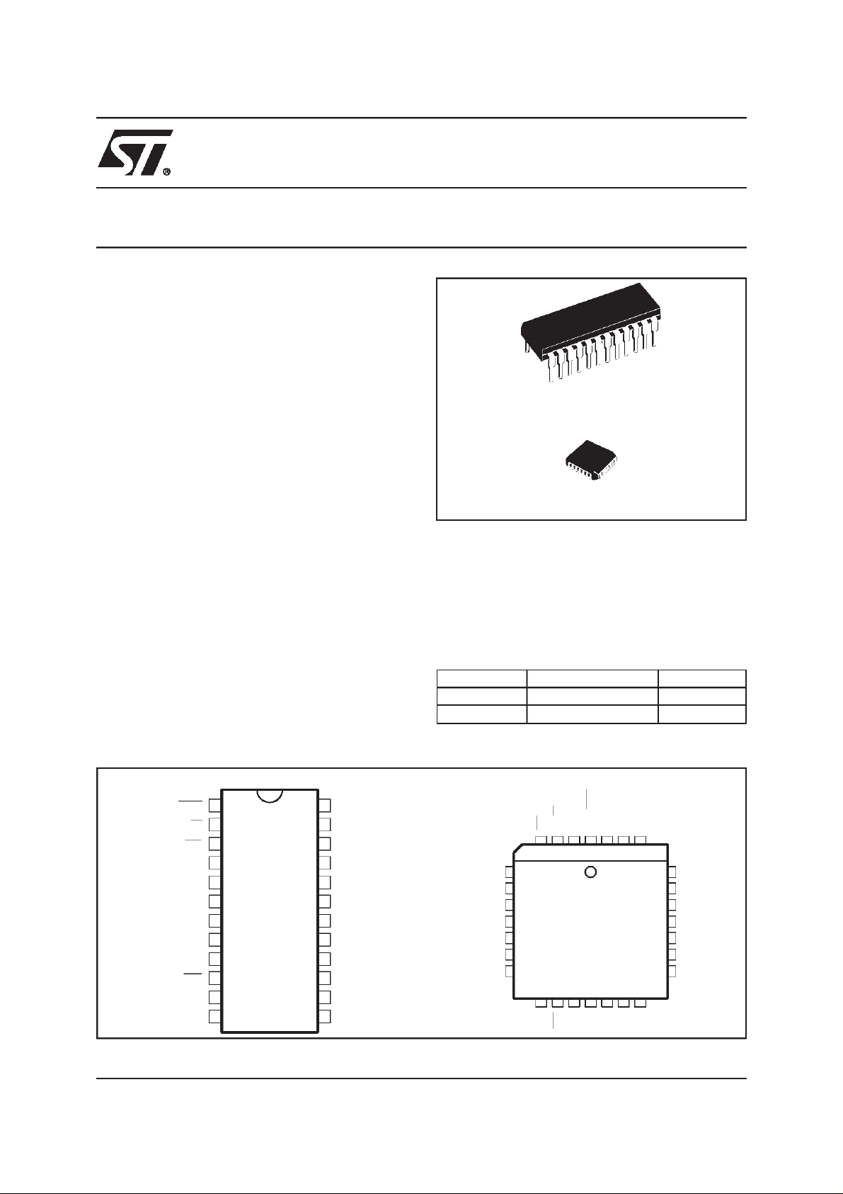
TS7514
DIP24
(Plastic Package)
PLCC28
(Plastic Leaded Chip Carrier Package)
ona 4-wireline. Itsprogrammingconceptmakesit
the ideal component to design low-cost intelligent
modems, featuring auto dialing and auto answering. The TS7514 conforms to CCITT V.23 recommendation. The chip incorporates DTMF dialing,
linemonitoring, tone and dialing detection.
DESCRIPTION
The TS7514 is an FSK modem which can be
programmed for asynchronous half-duplex voicebandcommunicationsona 2-wirelineorfullduplex
PIN CONNECTIONS
DIP24
MOD/DTMF
MC/BC
RTS
ENP
DGND
TxD
PRD
XTAL IN
XTAL OUT
DCD
RxD
ZCO
1
2
3
4
5
6
7
8
9
10
11
12
24
AXTL
23
WLO
22
ATO
21
V+
20
AGND
19
V-
18
RAO1
17
RAI1
16
RAI2
15
RAO2
14
RFO
13
RDI
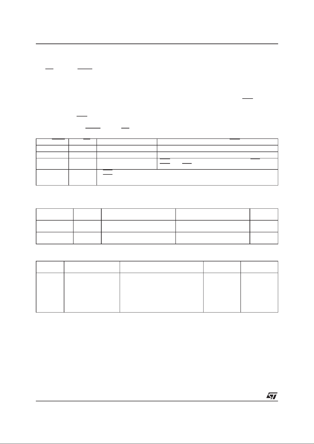
ORDER CODES
Part Number Temperature Range Package
TS7514CP 0 to 70
TS7514CFN 0 to 70
PLCC28
RTS
MC/BC
4
321
5
ENP
6
DGND
7
TxD
8
PRD
9
N/C
XTAL IN
10
11
12131415161718
N/C
DCD
o
C DIP24
o
C PLCC28
N/C
MOD/DTMF
ATXL
WLO
ATO
282726
RDI
RxD
ZCO
RFO
RAO2
25
V+
24
AGND
23
V-
22
RAO1
21
RAI1
20
RAI2
19
N/CXTAL OUT
7514-01.TBL
7514-01.EPS /7514-02.EPS
November 1998
1/19
TS7514
PIN DESCRIPTION
Name
MOD/DMTF 1 1 MODEM or DMTF Operating Mode Selection.
MC/BC 2 3 Digital Control Input.
RTS 3 4 Request to Send.
ENP 4 5
DGND 5 6 Digital Ground = 0V. All digital signals are referenced to this pin.
TxD 6 7 Digital Input for Transmit or Control Data
PRD 7 8 Digital Input for ControlData. Selected through ENP
XtaIIN 8 10 Crystal Oscillator Input. Can be tied to an external clock generator.
XtaIOUT 9 11 Crystal Oscillator Output
DCD 10 13 DataCarrier Detect Output
RxD 11 14 Digital Receive Data Output
ZCO 12 15 Zero Crossing Rx Digital Output (ringing detection)
RDI 13 16 Analog Output for the Receive Signal after Filtering or Analog Input for the
RFO 14 17 Analog Receive Filter Output
RAO2 15 18 A2 Amplifier Output
RAI2 16 20 A2 Amplifier Inverting Input
RAI1 17 21 A1 Amplifier Inverting Input
RAO1 18 22 A1 Amplifier Output
V- 19 23 Negative Supply Voltage : – 5V ±5%
AGND 20 24 Analog Ground = 0 V. Reference Pin for AnalogSignals
V+ 21 25 Positive Supply Voltage : + 5V ±5%
ATO 22 26 Analog Transmit Output
WLO 23 27 Analog Output for Line Monitoring and Buzzer
ATxI 24 28 Direct Analog Input Transmit Filter
Pin Number
DIP24 PLCC28
Description
Also controls write operations to control registers (if MOD/DMTF = 0 and
MC/BC= 0).
In MODEM mode, it sets transmission mode to main or back channel. It also
permits selection of dialing or control registers programming.
When RTS = 0, the circuit sends an analog signal to the ATO output.The signal
depends on the operating mode selected.
When RTS = 1,the signal sent to ATOis suppressedafter its firstzerocrossing.
When MOD/DMTF = 0 and MC/BC = 0, the RTS pin acts as a clock for serial
data loading into the input register.
Serial Register Write Select Input. When ENP = 0, the serial register input is
connected to TxD. When ENP = 1, the register input is connected to PRD.
QUARTZ
= 3.579MHz.
f
Amplifier-limiter.
7514-02.TBL
2/19
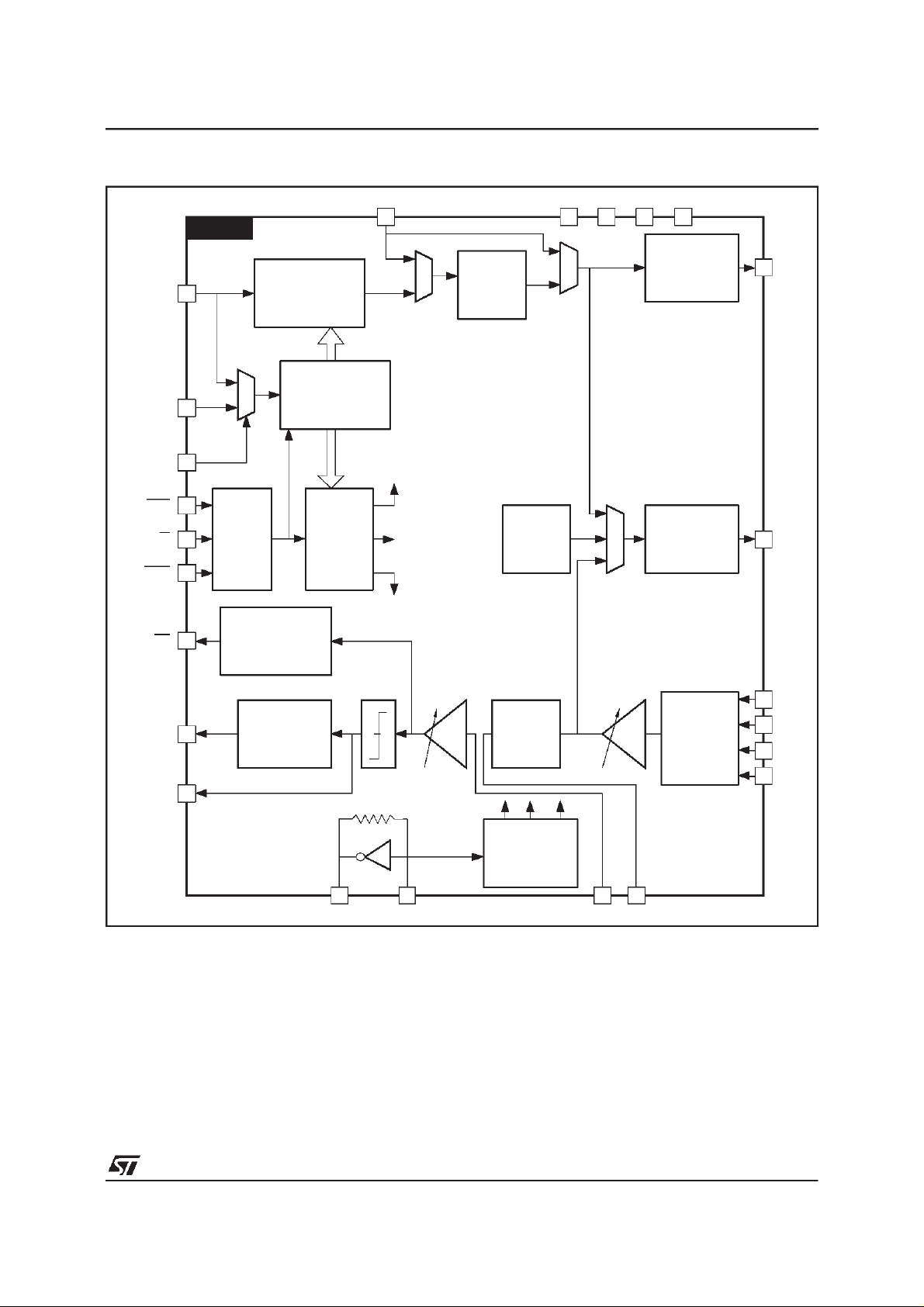
Figure1 : SimplifiedBlock Diagram
TS7514
TxD
PRD
ENP
RTS
MC/BC
MOD/DTMF
DCD
TS7514
Tx DATA
MODE
CARRIER/TONE
LEVEL DETECTOR
CARRIER/TONE
FREQUENCY
GENERATOR
INPUT SHIFT
CONTROL
REGISTER
CONTROL
REGISTERS
ATxI
DMTF DATA
TO
PROGRAMMABLE
FUNCTIONS
Tx
FILTER
V+ DGND V- AGND
ATTENUATOR
ATTENUATORBUZZER
ATO
WLO
RxD
ZCO
RX
DATA
FSK
DEMODULATOR
Xtal OUT Xtal IN
G
MASTER
CLOCK
Rx
FILTER
CLOCK
GENERATOR
G
RDI RFO
DUPLEXER
RAI1
RAO1
RAI2
RAO2
7514-03.EPS
3/19

TS7514
FUNCTIONAL DESCRIPTION
The TS7514 circuit is an FSK modem for half-duplex,voice-bandasynchronoustransmissions on a
2-wire line according to CCITT recommendation
V.23 or full duplexon 4 wire-line.
The circuit features DTMF dialing, call status tone
detection and line monitoring in both dialing and
automaticanswermodes. Asignallingfrequencyis
availableat the line monitoring output (buzzer).
Ring detection is possible by using the signal detection function and bypassing the receive filter.
Thereceive signal at ZCO outputcan befilteredin
the associated microprocessor.
TheTRANSMITchannel (Tx)includes :
- Twoprogrammablefrequencygenerators.
- Oneswitchedcapacitorfilter(SCF)withlow-pass
or bandpass configuration and its associated
propagationdelay corrector.
- Onecontinuous time low-passsmoothing filter.
- Oneattenuator,programmable from0 to + 13dB
by 1dB steps.
- Oneprogrammableanalog input.
TheRECEIVEchannel (Rx) includes:
- Two operational amplifiers for duplexer implementation.
- Onecontinuous time low-passanti-aliasingfilter.
- Oneprogrammablegain amplifier.
- Onelinear compromiseequalizer.
- One switchedcapacitor band pass filter (can be
set to eithermain or back channel).
- Onecontinuous time low passsmoothing filter.
- Onelimiting amplifier.
- Onecorrelationdemodulator.
- Oneprogrammablelevel signal detector.
Figure2 :
InternalControl Register
RTS
The LINE MONITORINGchannelincludes:
- One buzzer.
- One 3-channelmultiplexer to selectbeetwen:
- Transmitchannel monitoring.
- Receivechannel monitoring.
- Buzzer.
- One programmableattenuator
Internal Control
Power-upInitialization
TheTS7514includespower-upinitializationof control registers. This system sets the ATO transmission output to an infinite attenuation position,
leaving time for the microprocessor to set up the
RPROG input on power up. Control registers are
also initialized when V+ is lower than 3V or Vgreater than -3V.
Registers
WriteaccesstotheDTMFdataregisterandtoother
controlregistersis achievedinserialmodethrough
TxD input or PRD input. Addressing of these 4 bit
registersis indirect.They are accessedthroughan
8 bitshiftregisteraddressedwhenMOD/DTMF= 0
and MC/BC = 0. Data sent to the TxD input is
strobedon the RTS signal trailingedge.
Serial data is sent to the TxD input, with Least
Significant Bit (LSB) first. The 4 Most Significant
Bits (MSB) contain the control register address
while the4 LSB containassociated data.
Data transfer fromthe inputregister to the control
register(addressed bythe MSB’s)is startedby the
operating mode (MODEM or DTMF) selection
(MOD/DTMF= 1 or MC/BC= 1).
4/19
TxD or
PRD
Datas Addresses
CLK
8-BIT SHIFT REGISTER
(Input Register)
4-Bit Control
Register
RPROG
RDTMF
RATTE
RWLO
RPTF
RHDL
RPRX
RPROG
MOD/DTMF
MC/BC
RTS
TxD or PRD
D0 D1 D2 D3 D4 D5 D6 D7
Data Address
Time
7514-04.EPS
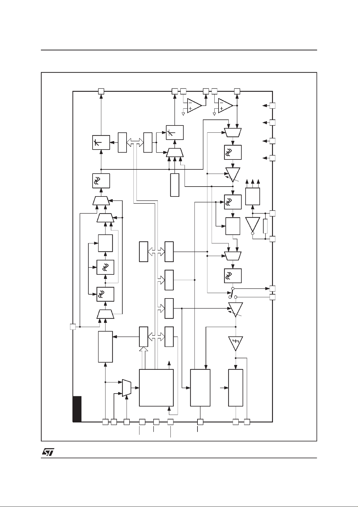
Figure3 : Detailed Block Diagram
TS7514
ATO
ATT
MX
MX RC
CORR
SCF
RATTE
RWLO
RPTF
4-bit Bus
RAI1
ATT
MX WLO
BUZZER
A1
Analog Loop
RAO1
RAI2
A2
RAO2
MX
RC
G
SCF
SCF
CORR
MX
5V 0V 0V -5V
Internal
Clocks
TIME
BASE
V+ AGND DGND V-
ATxL
Mode
TS7514
SCF
MX
FREQUENCY
GENERATOR
TxD
PRD
MX
ENP
RDTMF
Address
RTS
AND
DATA
REGISTER
SERIAL INPUT
MC/BC
Mode RPROG RHDL RPRX RPRF
Data
CONTROL
MOD/
DTMF
LEVEL
CARRIER
DETECTOR
DCD
Mode
RC
G
FSK
DEMODULATOR
RxD
ZCO
RDI RDO XTAL OUT XTAL IN
7514-05.EPS
5/19
TS7514
OPERATINGMODES
The various operating modes are defined by
MC/BCand MOD/DTMFinputs,andby thecontent
of a control register RPROG.
TheTS7514includes 8 controlregisters.Accessto
each control registeris achieved through an auxilliary8-bit shiftregister(input register).The input of
that shift register is connected either to TxD or
PRD,dependinguponthe statusof theENPcontrol
pin (ie when ENP = 0 and ENP = 1 respectively).
Inbothcases,theRTSinputreceivesthe shiftclock
and sequentialy transfer is controlled by setting
simultaneouslyMOD/DTMF and MC/BC to 0. The
previous internal status and data are memorized
duringloadingof the inputregistersothattransmission continues properly. That feature allows the
userto modifytransmissionlevelor linemonitoring
selection during transmission. The transmit channeloperatingmode(Modemmainor backchannel,
DTMF)canonly be modifiedwhenRTS =1. When
RTS = 0, the ATO transmit output is enabled and
thepreselectedoperatingmodeisactivated.When
RTSreturnsto 1, Modem or DTMF transmissionis
inhibited after the first zero crossing of the generated signal.
MOD/DTMF MC/BC Transmission
1 1 MODEM, Main Channel MODEM, Back Channel
1 0 MODEM, Back Channel MODEM, Main Channel
0 1 DTMF DCD= Active Tone Detection (270 -500Hz) if RTS = 1…
0 0 If RTS = 0 when that configuration occurs, transmission and reception are not modified.
Note 1 :
The decision thresholdof the demodulatoroutput is shifted, so thatRxD changes from 0 to 1 at 1950Hz instead of 1700Hz.
If RTS = 1 (no signal sent on the line), transmission is not modified and reception is set
up to detect 2100Hz tone (note 1).
(ATO)
DCD = 1 if RTS = 0
Reception
(RxD, DCD)
MODEMTRANSMISSIONFREQUENCIES
Modulation
Rate
75bps 1
1200bps 1
TxD
0
0
CCITT R35 AND V.23
Recommendations (Hz)
390 ±2
450 ±2
1300 ±10
2100 ±10
Frequency Generated with
Xtal at 3.579MHz (Hz)
390.09
450.45
1299.76
2099.12
DTMF TRANSMISSIONFREQUENCIES
Specifications
DTMF (Hz)
f1
f2
f3
f4
f5
f6
f7
f8
697 ±1.8%
770 ±1.8%
852 ±1.8%
941 ±1.8%
1209 ±1.8%
1336 ±1.8%
1477 ±1.8%
1633 ±1.8%
Frequency Generated with
Xtal at 3.579MHz(Hz)
699.13
771.45
853.90
940.01
1209.31
1335.65
1479.15
1627.07
Dividing Ratio Error (%)
5120
4640
4192
3808
2960
2680
2420
2200
Error (Hz)
+0.09
+0.45
-0.24
-0.88
+0.31
+0.19
+0.22
-0.10
+0.03
-0.03
+0.15
+0.36
6/19

TS7514
CARRIER LEVEL DETECTOR
- OutputLevel Detection conditions
The DCD signal detector output is set to logic
state 0 ifthe RMSvalueof thedemodulatorinput
signal is greater than N1. The DCD output has
logic state 1 if theRMS value is less than N2.
ModulationRatio DCD Transition CCITT V.23 (min) Min. Max. CCITT V.23 (max) Unit
1200bps t1
t2
75bps (Note 1) t1
t2
Note 1 : wide band Rx filterused (see Figure 7c).
10
15
The detectorhas an hysteresiseffect : N1 - N2.
- Timing Detection Requirements
Signal detection time constants at the DCD output complywith CCITTRecommendationV.23.
5
0
5
15
15
10
20
15
40
40
20
15
80
80
ms
ms
ms
ms
Figure4 :
Note :
PROGRAMMING REGISTER
D7 D6 D5 D4 D3 D2 D1 D0
X0000
SignalDetectionTime Out
N1
LINE
DCD
t
1
When delays arebypassed (see RPRX register programming) response time ranges from 0 to5ms in receivemode at 1200bps,
and from 0 to10ms at75bps.
t
2
N1
0V
(RPROG)
Address Data
X
0
X
0
1
0
The most significant bit (D7) is not used when decodingcontrol
1
register addresses.
Selected Mode (note 1)
0 X 0 1 Controlregister addressing is enabled when D7= 0(seenote2).
0 X 1 0 Controlregister addressing is enabled when D7= 1(seenote2).
0 0 X X Receptionpositionedinthe channeloppositetothe transmission
channel controlled by MC/BC
0 1 X X Reception positioned in the same channel as transmission
(see note 3).
1 X X X Programming inhibited in normal operating mode. This modeis
used for testing purposes.
Notes :
1. RPROG is setto 0000 on power-up.
2. Excepted for RPROGregister whose address is always 000, regardless of D0 and D1.
3. This mode allows either full duplex operation on a 4-wire line, or circuit testing with external Tx/Rx loopback.
7514-06.EPS
7/19

TS7514
DTMF DIALING DATA REGISTER
Address Data Tone Frequency (Hz)
D7 D6 D5 D4 D3 D2 D1 D0 Low High
P001XX00 697 X
X X 0 1 770 X
X X 1 0 852 X
X X 1 1 941 X
0 0 X X X 1209
0 1 X X X 1336
1 0 X X X 1477
1 1 X X X 1633
Notes : This register is notinitialized on power-up.
X : don’t care value.
P : 1,0 or X depending upon RPROG content.
DATAREGISTERFOR THETRANSMISSIONATTENUATOR
Address Data
D7 D6 D5 D4 D3 D2 D1 D0
P0100000 0 +4 –2
0001 1 +3
0010 2 +2 –4
0011 3 +1 –5
0100 4 0 –6
0101 5 –1 –7
0110 6 –2 –8
0111 7 –3 –9
1000 8 –4 –10
1001 9 –5 –11
1010 10 –6 –12
1011 11 –7 –13
1100 12 –8 –14
1101 13 –9 –15
1 1 1 0 Infinite < – 64 < – 70
1 1 1 1 Infinite* < – 64 * < –70 *
* Power-up configuration.
(RDTMFREGISTER)
Attenuation
(dB)
(RATE REGISTER)
Output Transmit
Level (dBm)
On Line Level (dBm)
CouplerGain (- 6dB)
LINEMONITORINGPROGRAMMINGREGISTER
Address Data
D7 D6 D5 D4 D3 D2 D1 D0
P0110000 –10
0001 –20
0010 –31
0011 –42
0100 0
0101 –10
0110 –20
0111 –31
1 0 0 0 0.42 V
1 0 0 1 – 10dB
1 0 1 0 – 20dB
1 0 1 1 – 31dB
1 1 X X < – 60dB*
* Power-up configuration.
Note :
Signaling frequencyis asquare wave signal at 2982Hz.
8/19
(RWLOREGISTER)
Line Monitoring In Transmit
Mode Relative Level (dB)
Line Monitoring In Receive
Mode Relative Level (dB)
PP

RECEIVEFILTERSELECTIONAND GAINPROGRAMMING REGISTER(RPRF REGISTER)
Address Data
D7 D6 D5 D4 D3 D2 D1 D0
P101XX00 0
XX01 +6*
XX10 +12
X X 1 1 0 RxChannel Band = Tx ChannelB andTx to
X 0 X X X Receive FilterSelected
X 1 X X X Receive FilterDesabled
1 X X X X Receive Filter Disconnected from RDI
* Power-up configuration.
Note 1 :
Depending on the line length, the received signal can be amplified. Programmablereception gain allows a levelclose to +3dBm
atthefilterinput to take benefit of the maximum filter dynamic range(S/N ratio). The following requirement must be met :
max. line level + prog. gain ≤+3dBm.
Reception Gain
(dB) (note 1)
Comments
Rx Loopback – 33dBm ≤ Rx Level ≤ 40dBm
Outp ut and from Demo dulat or . Off s e t
Disabled.
TS7514
TRANSMISSION FILTER PROGRAMMING REGISTER
Address Data
D7 D6 D5 D4 D3 D2 D1 D0
(RPTF REGISTER)
ATO Transmission
P 1 0 0 0 0 0 0 MODEM or DTMF Signal*
0 0 0 1 ATxI via Smoothing Filter andAttenuator
0 0 1 0 ATxI via Low-pass Filter and Attenuator
0 0 1 1 ATxI via Band-pass Filter andAttenuator
0 1 0 0 In DTMF Mode, Transmision of High Tone Frequency
1 0 0 0 In DTMF Mode, Transmission of Low Tone Frequency
* Power-up configuration.
HYSTERESIS AND SIGNALDETECTION LEVELPROGRAMMING REGISTER
Address Data
D7 D6 D5 D4 D3 D2 D1 D0
N2 (dBm) (note 1)
See Figure 4
(RHDLREGISTER)
N1/N2 (dB)
P110X000 –43* X
X001 –41 X
X010 –39 X
X011 –37 X
X100 –35 X
X101 –33 X
X110 –31 X
X111 –29 X
0XXX X 3*
1 X X X X 3.5
* Power-up configuration.
Note 1 :
Detection low level measured at the demodulator input. The line signal detection level is obtained by reducing the gain ate the filter.
9/19

TS7514
RECEIVECHANNEL PROGRAMMING REGISTER(RPRXREGISTER)
Address Data
D7 D6 D5 D4 D3 D2 D1 D0
P 1 1 1 X X 0 X Low Frequency Wide Band Selected (Figure 7b) (Note 1)
X X 1 X Low Frequency Narrow Band Selected (Figure 7c)
X X X 0 Carrier Level DetectorDelay Enabled*
X X X 1 Carrier Level DetectorDelay Disabled.
Note 1 : In active tone detection mode (MOD/DTMF= Ø, MC/BC = 1, RTS = 1 see op. modes),
The low frequencywide band is automatically selected for thereceivechannel, whatever the RPRX register programming value.
After a switch back to modem mode (MOD/DTMF = 1,MC/BC= Ø or 1) the RPRX register indicates again the value programmed
before the active tonedetection mode.
INPUTSHIFT REGISTER ACCESS
Figure5 : 1st Case: Programmationwithout Data Transmission
1
2
Configuration
Figure 6 :
RTS
MC/BC and MOD/DTMF
TxD or PRD
4
6
78
3
4
2nd Case : Programmationwith TxD During Data Transmission
RTS
MC/BC and
MOD/DTMF
TxD or PRD
Data
n1
Data
n
D0
D7
5
9
7514-07.EPS
56
1011 11
Data
n
7514-08.EPS
10/19

TS7514
ABSOLUTE MAXIMUMRATINGS
Symbol Parameter Value Unit
DGND DGND (digital ground) to AGND (analog ground) – 0.3, + 0.3 V
V+ Supply Voltage V+ to DGND ro AGND – 0.3, + 7 V
V– Supply Voltage V- to DGND or AGND – 7, + 0.3 V
V
I
V
in
I
o
I
out
P
tot
T
op
T
stg
T
lead
Ifthe Maximum Ratingsare exceeded, permanentdamage may be caused to the device. This is a stress rating only, and functionaloperation
ofthe device under these or anyother conditionsfor extendedperiodsmay affectdevice reliability.Standard CMOS handlingprocedures should
be employed to avoid possible damage to the device.
ELECTRIC OPERATING CHARACTERISTICS
Symbol Parameter Min. Typ. Max. Unit
V+ Positive Supply Voltage 4.75 5 5.25 V
V– Negative Supply Voltage – 5.25 – 5.0 – 4.75 V
I+ V+ Operating Current – 10 15 mA
I- V- Operating Current – 15 – 10 – mA
Voltage at any Digital Input DGND - 0.3, V+ + 0.3 V
Voltage at any Analog Input V– 0.3, V + + 0.3 V
Current at any Digital Output – 20, + 20 mA
Current at any Analog Output – 10, + 10 mA
Power Dissipation 500 mW
Operating Temperature 0, + 70 °C
Storage Temperature –65, + 150 °C
Lead Temperature (soldering, 10s) + 260 °C
7514-03.TBL
7514-04.TBL
DCAND OPERATING CHARACTERISTICS
Electrical characteristicsare guaranteedover thecomplete temperature range,with typical load unless
otherwisespecified.Typical valuesare given for : V
Symbol Parameter Test Conditions Min. Typ. Max. Unit
DIGITAL INTERFACE (MOD/DTMF, RTS, DCD, RxD, ZCO, TxD, MC/BC, ENP, PRD)
V
IL
V
IH
I
IL
I
IH
I
OL
I
OH
ANALOG INTERFACE-PROGRAMMABLE (ATxl)
V
in
I
in
C
in
R
in
ANALOG INTERFACE -TRANSMIT OUTPUT (ATO) (load conditions R
V
OS
C
L
R
L
V
out
R
out
– ATO Attenuation Ratio when RTS = 1 70 – – dB
Input Voltage, Low Level – – 0.8 V
Input Voltage, High Level – 2.2 – – –
Input Current, Low Level DGND < Vi<VIL(max) – 10 – 10 µA
Input Current, High Level VIH(min) < VI< V+ – 10 – 10 µA
Output Current, Low Level VOL= 0.4V 1.6 – – mA
Output Current, High Level VOH= 2.8V – – – 250 µA
Input Voltage Range – 1.8 – + 1.8 V
Input Current (filter output selected) – 10 – + 10 µA
Input Capacitance (ATT output selected) – – 20 pF
Input Resistance (ATT output selected) 100 – – kΩ
Output Offset Voltage – 250 – + 250 mV
Load Capacitance – – 100 pF
Load Resistance – 560 – Ω
Output Voltage Swing – 1.8 – + 1.8 V
Output Resistance 10 – 25 Ω
+
=+5V,V−= -5V and room temperature= 25oC
= 560Ω,CL= 100pF)
L
7514-05.TBL
11/19

TS7514
DCAND OPERATING CHARACTERISTICS
Electrical characteristicsare guaranteedover thecomplete temperature range,with typical load unless
otherwisespecified.Typical valuesare given for : V
(continued)
+
=+5V,V−= -5V and room temperature= 25oC
Symbol Parameter Test Conditions Min. Typ. Max. Unit
ANALOG INTERFACE -LINE MONITORING (WLO (load conditions , R
V
C
R
V
R
Output Offset Voltage – 250 – + 250 mV
OS
Load Capacitance – – 100 pF
L
Load Resistance 10 – – kΩ
L
Output Voltage Swing – 1.8 – + 1.8 V
out
Output Resistance – – 15 Ω
out
= 10kΩ,CL= 50pF)
L
– WLO Attenuation Ratio 70 – – dB
ANALOG INTERFACE -DUPLEXER (RAI+, RAI-, RA0)
V
C
V
V
C
R
Input Voltage Range RAI+, RAI– –2 – +2 V
in
Input Current RAI+, RAI– –10 – +10 µA
l
in
Input Capacitance RAI+, RAI– – – 10 pF
in
Input Offset Voltage RAI+, RAI– –20 – +20 mV
off
Output voltage Swing,RA0 CL= 100pF RL= 600Ω
out
Load Capacitance RA01 CL= 100pF – – 100 pF
L
Load Resistance RA01 300 – – Ω
L
G DC voltage Gain in Large Signals, RA01 C
= 300 Ω
R
L
= 100pF, RL= 300Ω 60 – – dB
L
–1.8
–0.9
–
–
+1.8
+0.9VV
CMRR Common Mode Rejection Ratio, RA01, RA02 60 – – dB
PSRR Supply Voltage Rejection Ratio, RA01, RA02 60 – – dB
V
C
R
AV
Output Voltage Swing, RA02 CL= 50pF, RL= 10kΩ –2.5 – 2.5 pF
out
Load Capacitance, RA02 – – 50 pF
L
Load Resistance, RA02 10 – – kΩ
L
DC Voltage Gain in Large Signals, RA02 – – dB
O
ANALOG INTERFACE-RECEIVE FILTER OUTPUT (RFO)
Amplifier Limiter Input (RDI)
V
R
C
C
R
V
R
Input Voltage Range (RPRF = 1 xxx) – 2.2 – + 2.2 V
in
Input Resistance (RPRF = 1 xxx) 1.5 – – kΩ
in
Input Capacitance (RPRF = 1 xxx) – – 20 pF
in
Load Capacitance (RPRF = 1 xxx) – – 50 pF
L
Load Resistance 1.5 – – kΩ
L
Output Voltage Swing CL= 50pF, RL= 1.5kΩ – 1.8 – + 1.8 V
out
Output Resistance – – 15 Ω
out
DYNAMIC CHARACTERISTICS FOR PROGRAMMING REGISTER ACCESS (see Figures 5 and 6)
t
(1) Cycle Time 600 – – ns
CYC
(2) Pulse Width, RTS Low 300 – – ns
P
wel
(3) Pulse Width, RTS High 300 – – ns
P
Weh
(4) RTSRise and Fall Times – – 50 ns
t
r,tf
(5) ControlInput HoldingTime 100 – – ns
t
HCE
(6) Control Input Setup Time 300 – – ns
t
SCE
(7) TxD or PRD InputSetup Time 200 – – ns
t
SDI
(8) TxD or PRD InputHold Time 100 – – ns
t
HDI
(9) TWW Input Writing Inpulsion Width (high level) 300 – – ns
t
WW
(10) TxD Input Setup Time 100 – – ns
t
BD
(11) TxD Input Hold Time 100 – – ns
t
HD
7514-06.TBL
12/19

TS7514
DCAND OPERATING CHARACTERISTICS(continued)
Electrical characteristicsare guaranteedover thecomplete temperature range,with typical load unless
otherwisespecified.Typical valuesare given for : V
Symbol Parameter Test Conditions Min. Typ. Max. Unit
TRANSMIT FILTER TRANSFER FUNCTION (load conditions : R
G
G
D
ATTENUATOR TRANSFER FUNCTION
A
R
R
TRANSMIT GENERAL CHARACTERISTICS
RECEIVE FILTER TRANSFERFUNCTION
G
G
G
G
G
G
Absolute Gain at 2100Hz – 0 – dB
AR
Gain Relative to Gain at 1700Hz Band-pass
HH
Group Delay (modem transmission)
AR
Main Channel : from 380 to 460Hz
Back Channel : from 1100 to 2300Hz
Absolute Gain for 0dB Programmed 0.3 0 0.3 dB
TT
Attenuation Relative toProgrammed Value
AT
Attenuation for Programmed Value = ∞
Relative Attenuation between two Consecutive Steps 0.8 - 1.2 dB
LT
Modem Amplitude (Att = 0dB) 390Hz
DTMF Amplitude (Att = 0dB)
- Low Frequency Group
- Low Frequency Group versus Low FrequencyGroup
Psophometric Noise – – 250 µV
Absolute Gain at 1100Hz - MainChannel
AR
(0dB programmed)
Gain Relative to the Gain at 1300Hz
RR
(0dB programmed)
Absolute Gain at 420Hz
AR
(back channel - narrow band) (0dB programmed)
Gain Relative to Gain at 420Hz (0dB programmed) < 150Hz
RR
Absolute Gain at 425Hz (tone detection or back
AR
channel wide band) (0dB programmed)
Gain Relative to Gain at 425Hz (0dB programmed) < 112Hz
RR
Psophometric Noise – – 300 µV
+
=+5V,V−= -5V and room temperature= 25oC
= 560Ω,CL= 100pF)
L
< 390Hz
= 390Hz
= 450Hz
= 1100Hz
–
–
–
- 0.5
–
–
–
–
+0.5
Band-pass or Low-pass
1100Hz to 2300Hz
3300Hz
5800Hz
> 16000Hz
- 0.5
–
–
–
–
–3
–
–
+0.5
90
1.04––
1.08µsms
- 0.570--+0.5 dB
450Hz
1300Hz
2100Hz
+3.5
+3.5
+3.5
+3.5
+1.5––
-3
–
+4.5
–
+4.5
–
+4.5
–
+4.5
-1.5
+2.5
– 0.5 – + 0.5 dB
< 150Hz
150Hz to 450Hz
1300Hz
2100Hz
2300Hz
5500Hz to 10000Hz
> 10000Hz
–
–
– 0.5
1.1
–
–
–
–
–
–
1.8
–
–
–
–60
–50
–50
–60
0.5 – + 0.5 dB
–
–
380Hz
400Hz to 440Hz
460Hz
1100Hz to 10000Hz
> 10000Hz
–
– 0.5
–
–
–
–50
–
+ 0.5
–
+ 0.5
–
+ 0.5
–
–50
–
–60
– 0.5 – + 0.5 dB
–
–
275Hz
300Hz to 525Hz
575Hz
1375Hz to 10000Hz
> 10000Hz
–
– 0.5
–
–
–
–50
–
+ 0.5
–
+ 0.5
–
+ 0.5
–
–50
–
–60
-30
-35
-35
–
-15
-35
110
0.5
2.3
2.7
dB
dB
dB
dB
dB
dB
dB
dB
dB
dBm
dBm
dBm
dBm
dBm
dB
dB
dB
dB
dB
dB
dB
dB
dB
dB
dB
dB
dB
dB
dB
dB
dB
dB
dB
dB
7514-07.TBL
13/19

TS7514
DCAND OPERATING CHARACTERISTICS(continued)
Electrical characteristicsare guaranteedover thecomplete temperature range,with typical load unless
otherwisespecified.Typical valuesare given for : V
Symbol Parameter Test Conditions Min. Typ. Max. Unit
RECEIVE TRANSFER - GENERAL CHARACTERISTICS
Absolute Filter Gain for :
0dB programmed
6dB programmed
12dBprogrammed
R
R
LINE MONITORING - GENERAL CHARACTERISTICS (load conditions : R
A
R
Signal Detection Level Relative to ProgrammedValue – 0.5 – + 0.5 dB
DS
Hysteresis Value – 2 – – dB
HY
Signal Level (loop3) at Reception Input – 40 – 35 – 33 dBm
Absolute Gain for 0dB Programmed – 0 – dB
TT
Attenuation Relative toProgrammed Value
AT
-
Attenuation for Programmed Value
FS Buzzer SignallingFrequency – 2982 – Hz
Signalling Frequency Amplitude at 0.42V
+
=+5V,V−= -5V and room temperature= 25oC
+ 11.5
= 10kΩ,CL= 50pF)
L
– 0.5
+ 5.5
–170–
–
–
–
+ 0.5
+ 6.5
12.5
+1 dB
–
Programmed 0.38 0.42 0.46 V
PP
dB
dB
PP
7514-08.TBL
14/19

TS7514
ReceiveFilter TransferCharacteristics
Figure7a : Main Channel
0
-10
-20
-30
-40
GAIN(dB)
-50
-60
-70
0.1 1 10 100
FREQUENCY (kHz)
Figure7b
GAIN(dB)
Figure7c
: BackChannel - NarrowBand
0
-10
-20
-30
-40
-50
-60
-70
0.1 1 10 100
FREQUENCY (kHz)
: Basic Channel
Wide band and Tone Detection
TransmissionSpectrum
At the ATO output, the out-of-band signal power
conformsto the following specifications:
0dB
25dB
f(kHz)
55dB
7514-09A.EPS
2001643.4
Receiver
Measurementconditions
Local transmitlevel : -10dBm on lower channelat
75bps.
Receive level : -25dBm, with 511 bit pseudo-randomtest pattern.
Testequipment : TRT sematest.
Isochronousdistortion
Thefollowing tableshowstypical isochronousdistortionobtainedwith the TS7514circuit :
Line Reception
(1200)
Line 1 (fiat) 10 % 4 %
Line 2 12 % 4 %
7514-09B.EPS
Line 3 18 % 6 %
Line 4 14 % 6 %
Reception
7514-10.EPS
(75)
0
-10
-20
-30
-40
GAIN(dB)
-50
-60
-70
0.1 1 10 100
FREQUENCY (kHz)
Bit error rate
Typical bit error rates versus while noise are as
follows(noiseandsignallevelsare measuredwithout weighting on the 300/3400Hz):
Reception
Line 1 6 dB 2.10
Line 2 7 dB 2.10
Line 3 8 dB 2.10
Line 4 7 dB 2.10
7514-09C.EPS
(1200)
S/N BER S/N BER
–3
– 3 dB 2.10
–3
– 3 dB 2.10
–3
– 3 dB 2.10
–3
– 3 dB 2.10
Reception
(75)
–3
–3
–3
–3
15/19

TS7514
CHARACTERISTICS OF TESTLINES
Figure8
10
5
0
0123kHz
Figure10
20
15
10
5
Figure 9
msCCETTLINE (FLAT)
2
10
5
1
0
0
7514-11.EPS
0 1 2 3 kHz
Figure11
msCCETTLINE 3 (90%)
4
3
2
1
20
15
10
5
msCCETTLINE 2 (10%)
2
1
0
7514-12.EPS
msCCETTLINE 2 (10%)
4
3
2
1
00
0123kHz
7514-13.EPS
00
0123kHz
7514-14.EPS
16/19

TYPICALAPPLICATION INFORMATION
+5V -5V
10µF10µF
++
External
Signal
100nF 100nF
V+ATxI GNDD GNDA V-
TxD
U.A.R.T.
RxD
C
O
PRD
RTS
T
S
7
N
MC/BC
5
1
M.C.U.
T
R
O
L
S
MOD/DTMF
ENP
DCD
ZCO
XTALOUT XTAL IN
4
RAO1
RAI1
ATO
RAI2
RAO2
WLO
RFO
RDI
Ω18kΩ
560
Ω12kΩ
560
100nF
(EMTL 162)
39kΩ
2.2µF
Transfo.
12kΩ
6.8kΩ
1µF
1.5kΩ
CTP 120Ω
(670 90003)
270k
To
Loudspeaker
Amplifier
TS7514
(*)
L1/TPH1
TRISIL
(TPA 270A 18)
Ω
L2
TPH2
EXTAL
(LS04)
(*) : RegulationRequired in France Only
12pF
3.579MHz
12pF
4.7kΩ
POWERSUPPLIESDECOUPLINGAND LAYOUTCONSIDERATIONS
Powersuppliesto digitalsystemsmay containhigh
amplitudespikes and othernoise.Tooptimize performancesof the TS7514 operatingin close proximity to digital systems, supply and ground noise
shouldbe minimized.
Thisinvolvesattentionto powersupply designand
circuitboard layout.
The power supplies should be bypassedwith tantalumor electrolyticcapacitorsto obtainnoise free
operation. These capacitors should be located
close to the TS7514. The electrolytic type capacitors for improved high frequencyperformance.
Power supplies connections should be short and
direct.Ground loopsshould be avoided.
2N2222
1N4148
+5V
7514-15.EPS
17/19

TS7514
PACKAGE MECHANICALDATA
24 PINS- PLASTICDIP
Dimensions
Min. Typ. Max. Min. Typ. Max.
Millimeters Inches
a1 0.63 0.025
b 0.45 0.018
b1 0.23 0.31 0.009 0.012
b2 1.27 0.050
D 32.2 1.268
E 15.2 16.68 0.598 0.657
e 2.54 0.100
e3 27.94 1.100
F 14.1 0.555
I 4.445 0.175
L 3.3 0.130
PM-DIP24.EPS
DIP24.TBL
18/19

PACKAGE MECHANICALDATA
28 PINS- PLASTICLEADED CHIP CARRIERPLCC)
TS7514
Dimensions
Min. Typ. Max. Min. Typ. Max.
Millimeters Inches
A 12.32 12.57 0.485 0.495
B 11.43 11.58 0.450 0.456
D 4.2 4.57 0.165 0.180
D1 2.29 3.04 0.090 0.120
D2 0.51 0.020
E 9.91 10.92 0.390 0.430
e 1.27 0.050
e3 7.62 0.300
F 0.46 0.018
F1 0.71 0.028
G 0.101 0.004
M 1.24 0.049
M1 1.143 0.045
Information furnished is believed to be accurate and reliable. However, STMicroelectronics assumes no responsibility for the
consequences of use of such information nor for anyinfringement of patents or other rights of third parties whichmay result from
its use. No licence is granted by implication or otherwise under any patent or patent rights of STMicroelectronics. Specifications
mentioned in this publication are subject to change without notice. This publication supersedes and replaces all information
previouslysupplied.STMicroelectronicsproductsare notauthorizedfor use ascriticalcomponentsinlifesupport devicesor systems
without express written approval of STMicroelectronics.
Purchase of I
Rights to use these components in aI
Australia - Brazil - Canada - China - France - Germany- Italy - Japan - Korea - Malaysia - Malta - Mexico - Morocco - The Netherlands
Singapore - Spain- Sweden - Switzerland - Taiwan - Thailand - UnitedKingdom - U.S.A.
The ST logo is a registered trademark of STMicroelectronics
1998 STMicroelectronics - All Rights Reserved
2
C Components of STMicroelectronics, conveys a license under the PhilipsI2C Patent.
2
C StandardSpecifications as defined by Philips.
the I
STMicroelectronics GROUP OF COMPANIES
2
C system,is granted provided that the system conformsto
http://www.st.com
19/19
PMPLCC28.EPS
PLCC28.TBL
 Loading...