

HMOS PARALLEL INTERFACE/TIMER
.TS68000 BUS COMPATIBLE
.PORT MODES INCLUDE:
BIT I/O
UNIDIRECTIONAL8 BIT AND 16 BIT
BIDIRECTIONAL8 BITAND 16 BIT
.PROGRAMMABLE HANDSHAKINGOPTIONS
.24-BIT PROGRAMMABLE TIMERMODES
.FIVE SEPARATE INTERRUPT VECTORS
.SEPARATE PORT AND TIMER INTERRUPT
SERVICE REQUESTS
.REGISTERSAREREAD/WRITEANDDIRECT-
LY ADDRESSABLE
.REGISTERS ARE ADDRESSED FOR MOVEP
(MovePeripheral) AND DMACCOMPATIBILITY
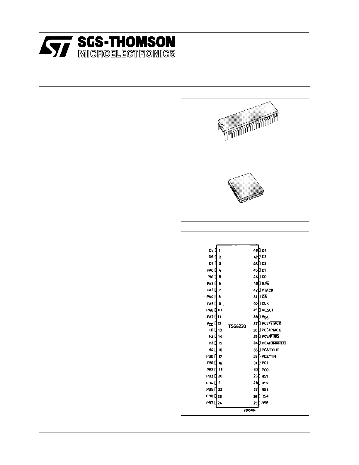
TS68 23 0
1
P
(PDIP48)
FN
(PLCC52)
DESCRIP TI ON
TheTS68230 parallelinterface/timer (PI/T)provides
versatile double buffered parallel interfaces and a
systemorientedtimerforTS68000 systems.Theparallelinterfaces operate inunidirectional orbidirectional modes, either 8 or 16 bits wide. In the
unidirectional modes, an associated data direction
register determines whether each port pinisaninput
or output. In the bidirectional modes the data direction registers are ignored and the direction isdetermined dynamically by the state of four handshake
pins. These programmable handshake pinsprovide
an interface flexible enough for connection to a wide
variety of low,medium, orhigh speedperipherals or
other computersystems.ThePI/Tports allow use of
vectored or auto-vectored interrupts, and also providea DMArequest pin for connection to the 68440
directmemory accesscontroller (DMAC)or a similar
circuit. The PI/Ttimercontains a 24-bit widecounter
anda 5-bit prescaler. The timermay beclocked by
the system clock (PI/T CLK pin) or by an external
clock(TINpin), and a 5-bit prescaler canbe used.It
can generate periodic interrupts, a square wave, or
a singleinterrupt aftera programmed time period. It
can also be used for elapsed time measurement or
asa device watchdog.
PIN CO N NECTI O N S
January1989
1/61

TS68230
SECT IO N 1
INTR ODU CTI ON
TheTS68230parallel interface/timer(PI/T)provides
versatile double buffered parallel interfaces and a
system oriented timer for TS68000 systems. The
parallel interfaces operate in unidirectional or bidirectionalmodes, either 8 or 16 bits wide. In the unidirectional modes, an associated data direction
registerdetermines whether eachport pinisaninput
or output. Inthe bidirectional modes the data direction registers are ignoredand thedirectionis determined dynamically by the state of four handshake
pins.Theseprogrammable handshakepinsprovide
an interface flexible enough forconnection toa wide
varietyoflow,medium, orhighspeedperipherals or
other computer systems. The PI/T ports allow use
ofvectoredor autovectored interrupts,and alsoprovide a DMArequest pin for connection tothe 68440
directmemoryaccesscontroller(DMAC)or asimilar
circuit.The PI/T timercontains a24-bitwide counter
and a 5-bit prescaler. The timer maybe clockedby
the system clock (PI/T CLK pin) or by an external
clock (TIN pin), and a 5-bit prescaler can be used.
It can generate periodic interrupts, a square wave,
ora singleinterrupt aftera programmed timeperiod.
It can also be used for elapsed timemeasurement
or as a devicewatchdog.
The PI/T consists of two logically independent sections : the ports and the timer. The port section
consistsofportA (PA0-PA7), port B(PB0-PB7), four
handshake pins (H1, H2,H3, and H4), twogeneral
input/output (I/O) pins, and six dual-function pins.
The dual-function pins can individually operate asa
thirdport (port C) or an alternate function relatedto
eitherport A, port B, or thetimer.The four programmable handshake pins, depending on the mode,
can control data transfer to and from the ports, or
can be used as interrupt generating inputs or I/O
pins. Refer to figure1.1.
The timer consists of a 24-bit counter, optionally
clocked by a 5-bit prescaler. Three pins provide
complete timer I/O : PC2/TIN, PC3/TOUT, and
PC7/TIACK. Only the ones needed for the given
configuration perform thetimerfunction,whilethe others remain port C I/O.
The system bus interface provides for asynchronoustransfer ofdata fromthe PI/T to a bus master
over the data bus (D0-D7). Data transfer acknowledge (DTACK), register selects (RS1-RS5), timer
interrupt acknowledge (TIACK), read/write line
(R/W), chip select (CS), or port interrupt acknowledge (PIACK) control data transfer between the
PI/T andan TS68000.
Features of the PI/T include :
.TS68000 Bus Compatible
.Port Modes Include:
Bit I/O
Unidirectional 8 Bit and 16 Bit
Bidirectional 8 Bit and 16 Bit
.Programmable Handshaking Options
.24-Bit Programmable Timer Modes
.Five Separate Interrupt Vectors
.Separate Port and Timer Interrupt Service
Requests
.Registersare Read/Write and Directly
Addressable
.Registersare Addressed for MOVEP(Move
Peripheral) and DMAC Compatibility
1.1.PORT MODEDESCRIPTION
The primary focus of most applications will be on
portA,port B,the handshake pins,theportinterrupt
pins, andthe DMArequest pin.They are controlled
inthefollowingway: theportgeneralcontrolregister
contains a 2-bit field that specifies one offour operationmodes.Thesegoverntheoverall operation of
the ports and determine their interrelation-ships.
Some modes require additional information from
eachport’s control register to further define its operation. In each port control register, there is a 2-bit
submode field that serves this purpose. Each port
mode/submode combination specifies a setof programmable characteristics that fully define the behavior of that port and two of the handshake pins.
This structure is summarized in table 1.1 and figure 1.2.
2/61
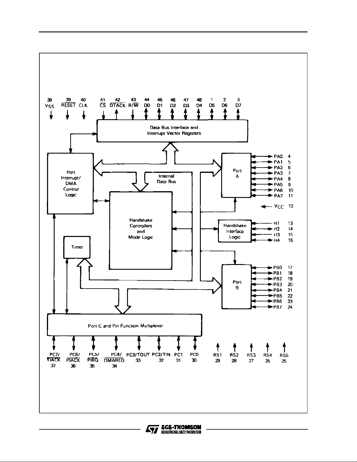
Figure 1.1 : Block Diagram.
TS68230
3/61

TS68230
Table1.1 :PortMode ControlSummary.
Mode 0 (unidirectional 8-bit mode)
Port A
Submode 00 - Pin-definable Double-buffered Input or Single-buffered Output
H1 - Latches Input Data
H2 - Status/interrupt Generating Input, General-purpose Output, or Operation with H1 in the Interlocked or
Pulsed Handshake Protocols
Submode 01 - Pin-definable Double-buffered Output or Non-latched Input
H1 - Indicates Data Received by Peripheral
H2 - Status/interrupt Generating Input, General-purpose Output, or Operation with H1 in the Interlocked or
Pulsed Handshake Protocols
Submode 1X - Pin-definable Single-buffered Output or non-latched Input
H1 - Status/interrupt Generating Input
H2 - Status/interrupt Generating Input or General-purpose Output
Port B
H3 and H4 - Identical to Port A, H1 and H2
Mode 1 (unidirectional 16-bit mode)
Port A - Most-significant Data Byte or non-latched Input or Single-buffered Output
Submode XX - (not used)
H1 - Status/interrupt Generating Input
H2 - Status/interrupt Generating Input or General-purpose Output
Port B - Least-significant Data Byte
Submode X0 - Pin-definable Double-buffered Input or Single-buffered Output
H3 - Latches Input Data
H4 - Status/interrupt Generating Input, General-purpose Output, or Operation with H3 in the Interlocked or
pulsed handshake Protocols
Submode X1 - Pin-definable Double-buffered Output or Non-latched Input
H3 - Indicates Data Received by Peripheral
H4 - Status/interrupt Generating Input, General-purpose Output, or Operation with H3 in the Interlocked or
Pulsed Hanshake Protocols
Mode 2 (bidirectional 8-bit mode)
Port A - Bit I/O
Submode XX - (not used)
Port B - Double-buffered Bidirectional Data
Submode XX - (not used)
H1 - Indicates Output Data Received by the Peripheral and Controls Output Drivers
H2 - Operation with H1 in the Interlocked or Pulsed Output Handshake Protocols
H3 - Latches Input Data
H4 - Operation with H3 in the Interlocked or Pulsed Input Handshake Protocols
Mode 3 (bidirectional 16-bit mode)
Port A - Double-buffered Bidirectional Data (most-signifiant data byte)
Submode XX - (not used)
Port B - Double-buffered Bidirectional Data (least-signifiant data byte)
Submode XX - (not used)
H1 - Indicates Output Data Received by the Peripheral and Controls Output Drivers
H2 - Operation with H1 in the Interlocked or Pulsed Output Handshake Protocols
H3 - Latches Input Data
H4 - Operation with H3 in the Interlocked or Pulsed Input Handshake Protocols
4/61
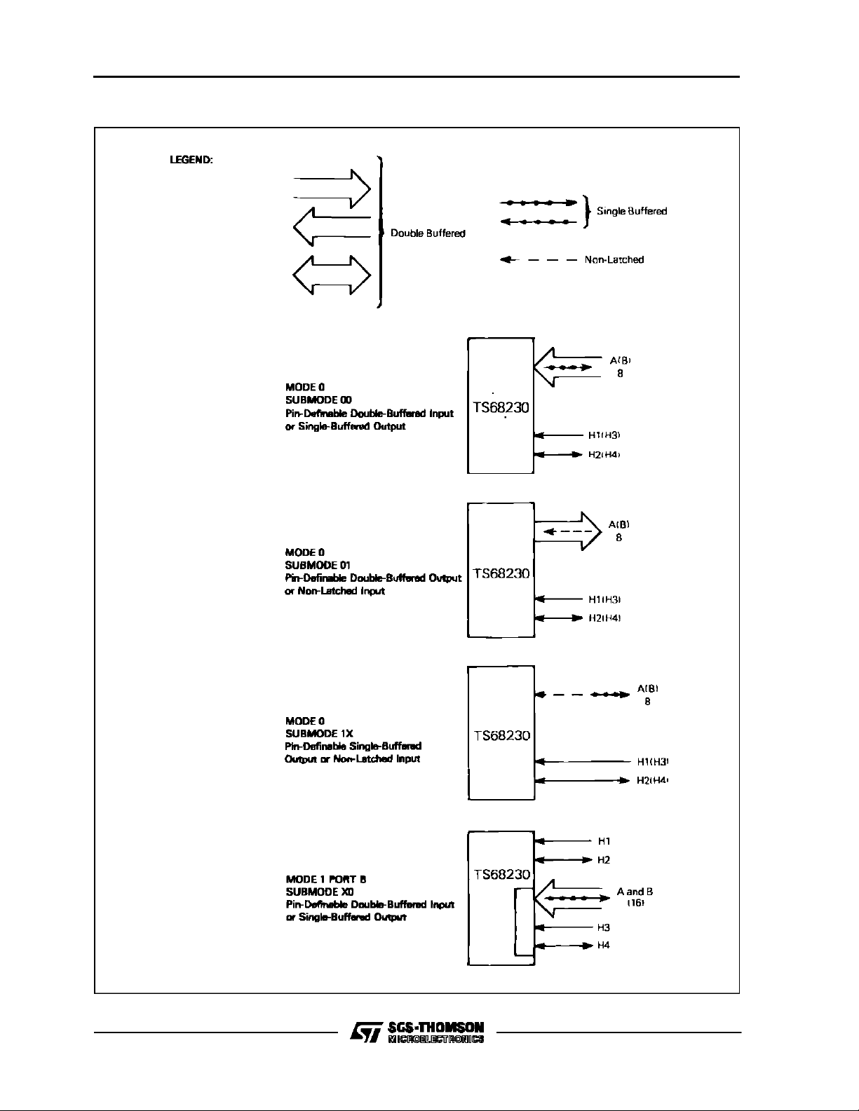
Figure 1.2 : Port Mode Layout.
TS68230
5/61

TS68230
Figure 1.2 : Port Mode Layout (continued).
1.2. SIGNALDESCRIPTION
Throughout thisdatasheet, signalsarepresented u-
sing the terms active and inactive or asserted and
negated independent ofwhether thesignal isactive
in the high-voltage state or low-voltage state. (The
activestate of each logic pin is given below). Active
low signals are denoted by a superscript bar. R/W
indicates a writeisactivelow anda readactivehigh.
Table1.2 further describes each pin and the logical
pin assignments are given in figure1.3.
6/61
1.2.1. BIDIRECTIONAL DATA BUS (D0-D7). The
data buspinsD0-D7 forman 8-bitbidirectionaldata
busto/fromanTS68000busmaster.Thesepins are
activehigh.
1.2.2.REGISTERSELECTS(RS1-RS5). Theregister select pins, RS1-RS5, are active high highimpedance inputs that determine which of the 23
internal registers is beingselected. They are provided by theTS68000 bus master or other bus master.

Table 1.2 :Signal Summary.
TS68230
SignalName Input/Output ActiveState
CLK Input Falling and Rising
CS Input Low Level
D0-D7 Input/output High = 1, Low = 0 Level High, Low, High Impedance
DMAREQ Output Low High, Low
DTACK Output Low High, Low, High Impedance*
H1(H3)*** Input Low or High Asserted Edge
H2(H4)** Input or Output Low or High Asserted Edge High, Low, High Impedance
PA0-PA7**, PB0-PB7**,
PC0-PC7
PIACK Input Low Level
PIRQ Output Low Low, High Impedance*
RS1-RS5 Input High = 1, Low = 0 Level
R/W Input High Read, Low Write Level
RESET Input Low Level
TIACK Input Low Level
TIN (external clock) Input Rising Edge
TIN (run/halt) Input High Level
TOUT (square wave) Output Low High, Low
TOUT (TIRQ) Output Low Low, High Impedance*
Input/output,
Input or Output
High = 1, Low = 0 Level High, Low, High Impedance
Edge/Level
Sensitive
Edge
Output States
* Pullup resistors required.
** Note these pins have internal pullup resistors.
Figure 1.3 : Logical Pin Connection.
7/61

TS68230
1.2.3. READ/WRITE (R/W). R/W is a high impedanceread/writeinput signalfrom theTS68000 bus
master, indicating whetherthe current bus cycle is
a read (high) or write (low) cycle.
1.2.4.CHIPSELECT (CS).CS isa high-impedance
input that selects the PI/T registers for the current
bus cycle. Addressstrobe and the data strobe(upper or lower) of the bus master,along with the appropriate address bits, must be included in the
chip-select equation. A low level correspondsto an
assertedchip select.
1.2.5. DATA TRANSFER ACKNOWLEDGE
(DTACK). DTACK is an active low output that signals the completion of the bus cycle. During read
orinterrupt acknowledge cycles,DTACKisasserted
afterdatahasbeen provided onthedatabus;during
writecyclesitisasserted afterdata hasbeen accepted at the data bus. Data transfer acknowledge is
compatible with the TS68000 and with other
TS68000 busmasterssuchasthe 68440 directmemory accesscontroller (DMAC). A pullupresistor is
required to maintainDTACK high between bus cycles.
1.2.6. RESET (RESET). RESET is a high-impedance input used to initialize all PI/T functions. All
controland data direction registers are cleared and
mostinternal operations are disabled by the assertion of RESET (low).
1.2.7.CLOCK (CLK). The clock pinis a high-impedance TTL-compatible signal with the same specifications as the TS68000. The PI/T contains
dynamiclogicthroughout, andhencethisclockmust
not be gatedoff atany time. It is not necessary that
thisclockmaintain any particular phase relationship
with the TS68000 system clock. It may be connected to an independent frequency source (faster or
slower)as longas allbus specificationsare met.
1.2.8.PORT A AND PORT B (PA0-PA7 AND PB0PB7). Ports A and B are 8-bit ports that may be
concatenatedto forma 16-bit port in certain modes.
The ports may be controlled inconjunction with the
handshake pinsH1-H4. Forstabilization duringsystempower up,portsAand Bhave internal pullupresistorsto VCC. Allports pins are active high.
1.2.9. HANDSHAKE PINS (H1-H4). Handshake
pins H1-H4 are multi-purpose pins that (depending
on the operational mode) may provide an interlocked handshake, a pulsed handshake, an interrupt input(independent of data transfers), or simple
I/O pins. For stabilization during system power up,
H2andH4 haveinternal pullup resistors toVCC. The
sense of H1-H4 (active high or low) may be programmed in the port general control register bits
3-0.Independent ofthemode,the instantaneous levelof the handshake pinscan beread from theport
status register.
1.2.10. PORT C (PC0-PC7/ALTERNATE FUNCTION).This port can be used as eight general purposeI/O pins (PC0-PC7) or any combination of six
special function pins and two general purpose I/O
pins (PC0-PC1). Each dual-function pin can be a
standardI/Oor aspecialfunctionindependent ofthe
otherport C pins. Whenused as a port C pin, these
pins are active high. They may be individually programmed as inputs or outputs by the port Cdata direction register. The dual-function pins are defined
in the following paragraphs.
The alternatefunctionsTIN, TOUT, and TIACK are
timerI/Opins.TINmaybeusedasarising-edge triggered external clock input or an external run/halt
controlpin (thetimer isin the run stateif run/halt is
high and in the halt state if run/halt is low). TOUT
may provide an active low timer interrupt request
outputor a general-purpose square-wave output, initially high. TIACKis an activelow high-impedance
inputused for timer interrupt acknowledge.
Port A and B functions have an independent pairof
activelowinterrupt request (PIRQ)and interrupt acknowledge (PIACK) pins.
The DMAREQ (direct memory access request) pin
provides an active low direct memory access controller request pulse for three clock cycles,completelycompatiblewith the 68440 DMAC.
8/61
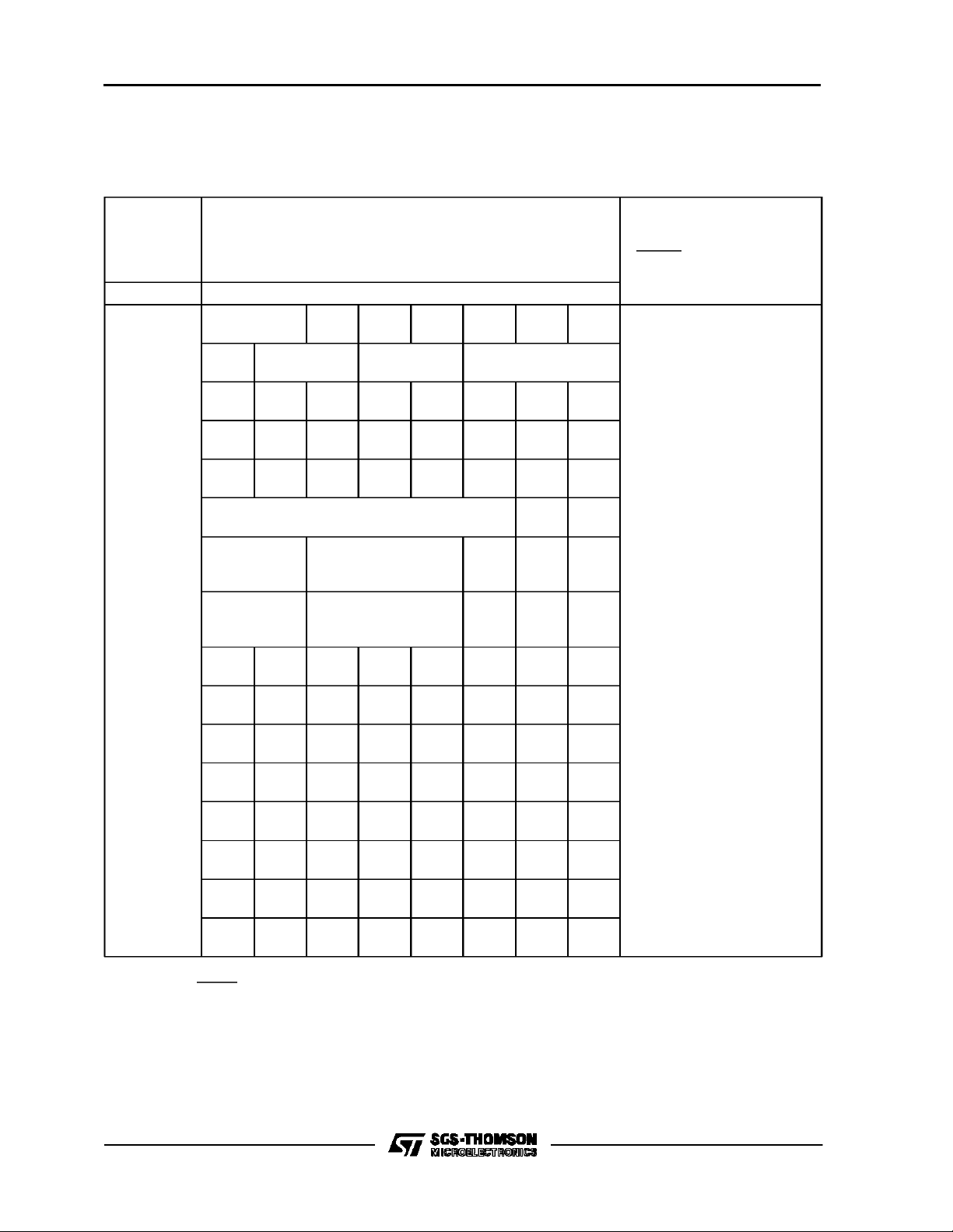
1.3. REGISTER MODEL
A registermodel that includes the corresponding register selectsis shown in table 1.3.
Table1.3 : Register Model.
Register
Register
SelectBits
5432176543210
0 0 0 0 0 Port Mode
Control
00001
00010 Bit7Bit
00011 Bit7Bit
00100 Bit7Bit
0 0 1 0 1 Interrupt Vector
0 0 1 1 0 Port A
0 0 1 1 1 Port B
01000 Bit7Bit
01001 Bit7Bit
01010 Bit7Bit
01011 Bit7Bit
01100 Bit7Bit
01101 H4
01110
V SVCRQ
Submode
Submode
LevelH3LevelH2LevelH1Level
VVVVVVVV 0 0 (null)
Select
6
6
6
6
6
6
6
6
H34
Enable
Bit
Bit
Bit
Bit
Bit
Bit
Bit
Bit
H12
EnableH4SenseH3SenseH2SenseH1Sense
IPF
Select
Bit
5
5
5
Number
5
5
5
5
5
4
Bit
4
Bit
4
H2 Control H2
H4 Control H4
Bit
4
Bit
4
Bit
4
Bit
4
Bit
4
Port Interrupt
Priority Control
Bit
3
Bit
3
Bit
3
Bit
Bit
Bit
Bit
2
2
2
1
Bit
1
Bit
1
Bit
0
Bit
0
Bit
0
VV 0 F Port Interrupt
H1
Int
SVCRQ
Enable
Enable
Bit
3
Bit
3
Bit
3
Bit
3
Bit
3
H4S H3S H2S H1S
Int
Bit
Bit
Bit
Bit
Bit
2
2
2
2
2
Enable
H3
SVCRQ
Enable
Bit
1
Bit
1
Bit
1
Bit
1
Bit
1
H1
Stat
Ctrl
H3
Stat
Ctrl
Bit
0
Bit
0
Bit
0
Bit
0
Bit
0
Value
after
RESET
(hex
value)
0 0 Port General
0 0 Port Service
0 0 Port A Data
0 0 Port B Data
0 0 Port C Data
0 0 Port A Control
0 0 Port B Control
VV Port A Data
VV Port B Data
VVV Port A Alternate
VVV Port B Alternate
VVVV Port C Data
VVVV Port Status
TS68230
Control Register
Request Register
Direction Register
Direction Register
Direction Register
Vector Register
Register
Register
Register
Register
Register
Register
Register
Register
01111
VVVVVVVV 0 0 (null)
* Unused, read as zero.
** Val ue before RESET.
*** C urrent value o n p ins.
9/61

TS68230
Table1.3 : Register Model (continued).
Register
SelectBits
5432176543210
1 0 0 0 0 TOUT/TIACK
Control
10001 Bit7Bit
6
10010
VVVVVVVV 0 0 (null)
Bit
ZD
Ctrl
Bit
5
4
V Clock
Control
Bit
3
Bit
2
Bit
Timer
Enable
Bit
1
0
Register
Value
after
RESET
(hex
value)
0 0 Timer Control
Register
0 F Timer Interrupt
Vector Register
10011 Bit23Bit
22
10100 Bit15Bit
14
10101 Bit7Bit
10110
10111 Bit23Bit
11000 Bit15Bit
11001 Bit7Bit
11010
11011
11100
11101
11110
VVVVVVVV 0 0 (null)
22
14
VVVVVVVZDS 0 0 Timer Status
VVVVVVVV 0 0 (null)
VVVVVVVV 0 0 (null)
VVVVVVVV 0 0 (null)
VVVVVVVV 0 0 (null)
Bit
21
Bit
13
Bit
6
6
5
Bit
21
Bit
13
Bit
5
Bit
20
Bit
12
Bit
Bit
20
Bit
12
Bit
Bit
19
Bit
11
Bit
4
4
3
Bit
19
Bit
11
Bit
3
Bit
18
Bit
10
Bit
Bit
18
Bit
10
Bit
Bit
17
Bit
9
Bit
2
2
1
Bit
17
Bit
9
Bit
1
Bit
16
Bit
Bit
Bit
16
Bit
Bit
VV Counter Preload
Register (high)
VV Counter Preload
8
Register (mid)
VV Counter Preload
0
Register (low)
VV Count Register
(high)
VV Count Register
8
(mid)
VV Count Register
0
(low)
Register
11111
VVVVVVVV 0 0 (null)
* Unused, read as zero.
10/61

TS68230
1.4. BUS INTERFACE OPERATION
The PI/Thas anasynchronous businterfaceprima-
rilydesigned for usewithan TS68000 microprocessor.With care,however, itcan beconnected tosynchronous microprocessor buses. This section
completelydescribes thePI/T’sbus interface,andis
intended for the asynchronous busdesigner unless
otherwise mentioned.
Inan asynchronous systemthePI/T clock mayoperate at a significantlydifferent frequency, either higherorlower,thanthebusmasterandothersystem
components, as long as all bus specifications are
met. TheTS68230 CLK pin hasthesame specificationsas the TS68000 CLK pin, andmust not begated off at any time.
The following signals generate normal read and
write cycles to the PI/T : CS (chip select), R/W
(read/write), RS1-RS5(five register select bits), D0D7 (the 8-bit bidirectional data bus), and DTACK
(data transfer acknowledge). To generate interrupt
acknowledge cycles, PC6/PIACK or PC7/TIACK is
usedinstead of CS, andthe register select pinsare
ignored. No combination of the following pin functionsmay be asserted simultaneously : CS, PIACK,
or TIACK.
1.4.1.READCYCLES. Thiscategory includesallregisterreads, except port or timer interrupt acknowledgecycles. WhenCS is asserted, theregister select and R/W inputs are latched internally. They
mustmeet smallsetup and hold timerequirements
with respect to the asserted edge of CS. (Refer to
6.6 AC Electrical Specifications for further information). The PI/T is not protected againstaborted
(shortened) bus cyclesgenerated byan address error or bus errorexception in which it is addressed.
Certain operations triggered by normal read (or
write)buscyclesarenot complete withinthe timeallotted to the bus cycle. One example is transfers
to/from the double-buffered latches that occur as a
result of the bus cycle. If the bus master’s clock is
significan-tly faster than the PI/T’s the possibility
exists that, following the bus cycle, CS can be negated then re-asserted before completion of these
internaloperations.InthissituationthePI/Tdoes not
recognize there-assertion of CSuntilthese operations are complete. Only at that time does it begin
theinternalsequencing necessaryto reacttotheasserted CS. Since CS also controls the DTACK response, this ”buscycle recovery time” can be related to the clock edge on which DTACK is asserted
for that cycle. The PI/T will recognize the subsequent assertionofCSthreeclockperiodsafterthe
clockedge on which DTACKwas previously asserted.
The register select andR/W inputspass through an
internal latchthat is transparent when the PI/T can
recognize a new CS pulse (see above paragraph).
Since the internal data bus of the PI/T is continuouslyengaged forreadtransfers, thereadaccess
time(tothe databus buffers)begins whentheregister selects are stabilized internally. Also, when the
PI/Tis ready tobegina newbus cycle,the assertion
of CS enables the data bus buffers within a short
propagation delay.Thisdoesnotcontribute tothe overall read access time unless CSis assertedsignificantlyafter the register select and R/W inputs are
stabilized (as may occur with synchronous bus
microprocessors).
Inaddition tothe chipselect’spreviously mentioned
duties, it controls the assertion of DTACK and latchingof read data at the data bus interface. Except
for controlling input latches and enabling the data
busbuffers,allofthesefunctionsoccuronlyafterCS
has been recognized internally and synchronized
withthe internal clock. Chip select isrecognized on
the falling edge of the clock if the setup time is met
; DTACK is asserted (low) on the next falling edge
of the clock. Read datais latched at the PI/T’s data
bus interface at the sametime DTACKis asserted.
It is stable as long as chip select remains asserted
independent of other external conditions.
Fromthe above discussion it isclear that if the chip
selectsetuptimeprior tothefallingedgeofthe clock
is met, the PI/T can consistently respond to a new
reador write bus cycleevery four clock cycles.This
factis especially usefulin designing the PI/T’sclock
in synchronous bus systems not using DTACK. (An
extra clock period is required in interrupt acknowledge cycles, see 1.4.2 Interrupt Acknowledge
Cycles).
In asynchronous bus systems in which the PI/T’s
clock differs from that of the bus master, generally
thereisno waytoguarantee thatthechip select setup time with respect to the PI/T clock is met. Thus,
the only way to determine that the PI/T recognized
the assertion of CS is to wait for the assertion of
DTACK.In thissituation,alllatchedbusinputstothe
PI/T must be held stable until DTACK is asserted.
These include register select, R/W, and write data
inputs (see below).
System specifications impose a maximum delay
fromthe trailing(negated) edgeofCS tothenegated
edgeofDTACK. Assystemspeedsincreasethisbecomesmoredifficult to meetwith asimplepullup resistor tied to the DTACK line. Therefore, the PI/T
provides an internal active pullup deviceto reduce
the rise time, and a level-sensitive circuit that later
turns this device off. DTACK is negated asynchronouslyas fast as possiblefollowing the rising edge
11/61

TS68230
of chip select, then three-stated to avoid interferencewith the nextbus cycle.
The systemdesignermust takecare thatDTACK is
negated andthree-statedquicklyenough aftereach
bus cycle to avoid interference with the next one.
With an TS68000this necessitates a relatively fast
external path from the data strobe negation to CS
bus master negation.
1.4.2. INTERRUPT ACKNOWLEDGE CYCLES.
Special internal operations take placeon PI/T interrupt acknowledge cycles. The port interrupt vector
register or the timer vector register are implicitly addressed by the assertion of PC6/PIACK or
PC7/TIACK, respectively. The signals are first synchronized with the falling edge of the clock. One
clockperiod after they arerecognized, thedata bus
buffers areenabled andthe vectorisdrivenontothe
bus. DTACK is assertedafter another clock period
toallowthe vector somesetuptimeprior toDTACK.
DTACK is negated, then three-stated, as with normal read or write cycles,when PIACK or TIACK is
negated.
1.4.3.WRITE CYCLES. In manyways, writecycles
are similar to normal read cycles. On write cycles,
data at the D0-D7 pins must meet the same setup
specificationsas the register select and R/W lines.
Like these signals, write data is latched on the asserted edgeof CS,and must meet small setup and
hold time requirements with respect to that edge.
The samebus cyclerecovery conditions existas for
normal read cycles.No other differences exist.
12/61

SECT IO N 2
TS68230
PORT GENERAL INFORM AT ION AND
CONVENTI O NS
This sectionintroduces concepts that are generally
applicable to the PI/Tports independent ofthe chosen mode and submode. For this reason, no particular port or handshake pins are mentioned ; the
notation H1(H3) indicates that, depending on the
chosen mode and submode, the statement given
may be true for either the H1or H3 handshake pin.
2.1. UNIDIRECTIONALVS BIDIRECTIONAL
Figure 1.2showsthe configuration of portsA and B
and each of the handshake pinsin each port mode
andsubmode.In modes0and 1,adatadirectionregisteris associatedwith eachoftheports. These registerscontainonebitfor eachport pinto determine
whether that pin is an input or an output. Modes 0
and 1 are, thus, called unidirectional modes becauseeach pinassumes aconstantdirection, changeableonly by a resetcondition or a programming
change. These modes allow double-buffered data
transfersinonedirection. Thisdirection, determined
by the mode and submode definition, is known as
the primary direction. Data transfers in the primary
directionare controlledbythehandshake pins. Data
transfers not in the primary direction are generally
unrelated, andsingleorunbuffered datapathsexist.
In modes 2 and3 thereis no concept of primary direction as in modes 0 and 1. Except for port A in
mode2 (bit I/O),thedatadirectionregisters haveno
effect. These modesare bidirectional, in thatthe directionof each transfer(always 8 or 16 bits,double
buffered) is determined dynamically by the state of
thehandshakepins.Thus,forexample, datamaybe
transferred out of the ports, followed very shortlyby
a transfer into the same port pins. Transfers to and
from the ports are independent and may occur in
any sequence. Since the instantaneous direction is
always determined by the external system, a small
amount of arbitration logic may be required.
2.1.1.CONTROL OF DOUBLE-BUFFERED DATA
PORTS. Generally speaking, the PI/T is a doublebuffereddevice.Intheprimarydirection, doublebuffering allows orderly transfers by using the handshakepinsin anyofseveral programmable protocols.
(When bit I/O is used, double buffering is not available and the handshake pins are used as outputs
or status/interrupt inputs).
Use of double buffering is most beneficial in situations where a peripheral device and the computer
system are capable of transferring data at roughly
the samespeed. Double bufferingallows the fetch
operation of the data transmitter to be overlapped
with the store operation of the data receiver. Thus,
throughput measured inbytesor words-per-second
may be greatly enhanced. If there is a large mismatch in transfer capability between the computer
and the peripheral, little or no benefit isobtained. In
these cases there isno penalty in using double buffering.
2.1.2. DOUBLE-BUFFERED INPUTTRANSFERS.
Inall modes, thePI/Tsupports double-buffered input
transfers. Data that meets the port setupand hold
times is latched on the asserted edge of H1(H3).
H1(H3) isedgesensitive, and mayassumeanyduty
cycleaslongasbothhighandlowminimumtimesare
observed. The PI/T contains a port status register
whose H1S(H3S) statusbit is set anytime any input
datathathasnot beenread bythe busmasterispresent in the double-buffered latches. The action of
H2(H4) is programmable ; it may indicate whether
thereis room for more data in the PI/T latches or it
mayserveotherpurposes. Thefollowingoptions are
available, depending on the mode.
1. H2(H4) may be anedge-sensitive input that is
independent ofH1(H3)andthe transferof port
data. On the asserted edge of H2(H4), the
H2S(H4S) status bit is set. It is clearedby the
direct method (refer to 2.3 Direct Method of
Resetting Status), the RESET pin being asserted,or when the H12 enable (H34 enable)
bit of the portgeneral control register is zero.
2. H2(H4) may be a general purpose output pin
that is always negated. The H2S(H4S) status
bit is always zero.
3. H2(H4) may be a general purpose output pin
thatis always asserted. The H2S(H4S)status
bit is always zero.
4. H2(H4)maybe an output pinin theinterlocked
input handshake protocol. It is asserted when
the port input latches are ready to accept new
data.Itisnegated asynchronously followingthe
asserted edge of theH1(H3)input. As soonas
the input latches become ready, H2(H4) is again asserted. When both double-buffered
latches are full, H2(H4) remains negated until
dataisremovedbyareadofportA(portB)data
register.Thus,anytimetheH2(H4)output isasserted, new input data may be entered by asserting H1(H3). At other times transitions of
H1(H3) areignored. TheH2S(H4S)statusbitis
alwayszero.WhenH12enable(H34 enable) is
zero,H2(H4) is heldnegated.
13/61
TS68230
5. H2(H4) maybe anoutput pin in thepulsed input handshake protocol. It is asserted exactly
as in the interlocked input protocol, but never
remains asserted longer than four clock cycles. Typically, a four clock cycle pulse is generated. But in the case that a subsequent
H1(H3)asserted edge occursbefore terminationof the pulse, H2(H4)is negated asynchronously.Thus,anytimeaftertheleading edgeof
the H2(H4) pulse, new data maybe entered in
the PI/T double-buffered input latches. The
H2S(H4S)statusbit isalwayszero. WhenH12
enable(H34enable) iszero,H2(H4)isheldnegated.
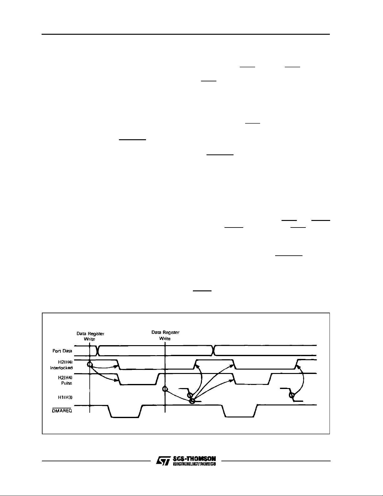
2.1.3. DOUBLE-BUFFERED OUTPUT TRANSFERS. The PI/T supports double-buffered output
transfers inall modes. Data, written bythebus mastertothePI/T,isstoredin theport’soutputlatch.The
peripheral accepts the data by asserting H1(H3),
whichcausesthe nextdatatobemovedto theport’s
output latch as soon as it is available. The function
ofH2(H4)isprogrammable ;it mayindicatewhether
data has been moved to the output latch or it may
serveotherpurposes.TheH1S(H3S)statusbitmay
be programmed for two interpretations. First, the
status bit is a one when there is atleast one latchin
the double-buffered data path that can accept new
data.Afterwritingone byte/wordofdatatotheports,
aninterruptserviceroutinecouldcheckthisbittodetermineifitcouldstoreanother byte/word, thus filling
both latches. Second, whenthe bus master is finished, itis oftenuseful to be ableto checkwhetherall
of the data has been transferred to the peripheral.
The H1S(H3S) status bit is set when both output
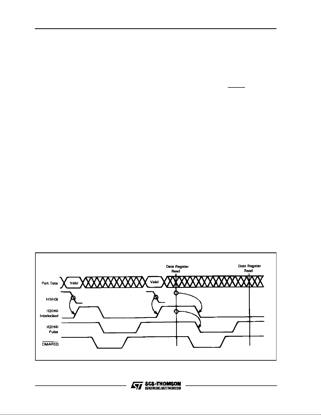
Figure 2.1 : Double-Buffered Input Transfers Timing Diagram.
latchesareempty.The programmableoptionsofthe
H2(H4) pin are given below, depending on the
mode.
1. H2(H4) may bean edge-sensitive input pinin-
2. H2(H4) may be a general-purpose output pin
3. H2(H4) may be a general-purpose output pin
4. H2(H4)maybe anoutputpinintheinterlocked
dependent of H1(H3) and the transfer of port
data. On the asserted edge of H2(H4), the
H2S(H4S) status bit is set. It is clearedby the
direct method (refer to 2.3 Direct Method of
Resetting Status), the RESET pin being asserted,or when the H12 enable (H34 enable)
bit of the portgeneral control register is zero.
thatis alwayszero.
that is always asserted.The H2S(H4s)status
bit is always zero.
output handshake protocol. H2(H4) is assertedtwo clockcyclesafterdata istransferred to
the double-buffered output latches. The data
remains stable and H2(H4) remains asserted
until the next asserted edge of the H1(H3) input.Atthattime,H2(H4) isasynchronously negated.As soonas the next datais available, it
is transferred tothe output latches andH2(H4)
is asserted. When H2(H4) is negated, assertedtransitionson H1(H3)have noeffect onthe
data paths. As is explained later, however, in
modes2 and 3 H1does controlthethree-state
output buffers of the bidirectional port(s). The
H2S(H4S)statusbitisalwayszero.WhenH12
enable(H34enable)is zero,H2(H4) isheldnegated.
14/61
TS68230
5. H2(H4)maybe anoutput pininthe pulsed output handshake protocol. It is asserted exactly
asintheinterlocked outputprotocol above,but
neverremains asserted longer than fourclock
cycles.Typically, a four clockpulse is generated.But in the case that a subsequent H1(H3)
assertededge occursbeforeterminationof the
pulse, H2(H4) is negated asynchronously,
thus shortening the pulse. The H2S(H4S) status bit is alwayszero. When H12 enable (H34
enable) is zero, H2(H4) is held negated.
A sampletiming diagram isshownin figure2.2.The
H2(H4) interlocked and pulsed output handshake
protocols are shown. The DMAREQ pin is also
shown assuming it is enabled. All handshake pin
sense bits are assumed to be zero ; thus,the pins
arein the lowstate whenasserted.Due to thegreat
similaritybetweenmodes, thistimingdiagram isapplicable to all double-buffered output transfers.
2.2. REQUESTING BUS MASTER SERVICE
The PI/Thas severalmeans of indicating a need for
service by a bus master. First, the processor may
poll the port status register. It contains a status bit
for each handshake pin, plus a level bit that always
reflects the instantaneous state of that handshake
pin.Astatusbit isonewhenthePI/Tneedsservicing
(i.e., generally when the bus masterneeds to read
or write data to the ports)or whena handshake pin
used as a simple status input has been asserted.
The interpretation of these bitsis dependent on the
chosen modeand submode.
Second, the PI/T may be placedin the processor’s
interrupt structure. As mentioned previously, the
PI/T contains port A and B control registers that
configure thehandshakepins.Otherbitsintheseregisters enable an interrupt associated with each
handshake pin. This interrupt is made available
through the PC5/PIRQ pin, if the PIRQ function is
selected. Three additional conditions are required
for PIRQto be asserted : 1) the handshake pin status bitis set, 2) the corresponding interrupt (service
request) enable bit is set,and 3) DMA requests are
not associated with that data transfer (H1 and H3
only). The conditions from each of the four handshake status bits and corresponding status bits are
ORedto determine PIRQ.Toclearthe interrupt, the
proper status bit must be cleared (see 2.3. Direct
Methodof Resetting Status).
The third method of requesting service is via the
PC4/DMAREQ pin. This pin canbe associatedwith
double-buffered transfersin eachmode. If itis used
as a DMA controller request, it can initiate requests
to keep the PI/T’s input/output double-buffering
empty/fullasmuchaspossible.Itwillnot overrunthe
DMA controller. The pin is compatible with the
68440direct memory access controller(DMAC).
2.2.1. VECTORED, PRIORITIZED PORT INTERRUPTS.Use ofTS68000compatible vectoredinterrupts with the PI/T requires the PIRQ and PIACK
pins.When PIACKis asserted while PIRQ is asserted,the PI/T places an 8-bit vector on the datapins
D0-D7.Under normalconditions, this vector correspondsto the highest priority enabled active port interrupt source with which the DMAREQ pin is not
currently associated. The most-significant six bits
are provided by the port interrupt vector register
(PIVR), with the lower two bits supplied by prioritization logic according to conditions present when
PIACKis asserted.It isimportant tonotethattheon-
Figure 2.2 : Double-Buffered OutputTransfers TimingDiagram.
15/61
TS68230
ly effect on the PI/T caused by interrupt acknowledgecycles is that the vectoris placed on the data
bus. Specifically, no registers, data,status, or other
internal states of the PI/T are affectedby the cycle.
Several conditions may bepresentwhenthe PIACK
inputis assertedto thePI/T. These conditionsaffect
the PI/T’sresponse and the termination of the bus
cycle.If thePI/T has no interrupt function selected,
or is not asserting PIRQ, the PI/Twill make no responsetoPIACK(DTACKwillnot beasserted). Ifthe
PI/Tis asserting PIRQwhen PIACKis received, the
PI/Twilloutputthecontentsoftheport interrupt vectorregisterandthe prioritization bits.Ifthe PIVRhas
not been initialized, $0F will be read fromthis register.These conditions are summarized in table 2.1.
The vector table entries for the PI/T appear as a
contiguous block of four vector numbers whose
commonuppersixbitsare programmed inthePIVR.
The following table pairs each interrupt sourcewith
the 2-bit value provided by the prioritization logic
when interrupt acknowledge is asserted (see 4.2.
Port Service Request Register (PSRR)).
H1 source - 00 H2 source - 01
H3 source - 10 H4 source - 11
2.2.2. AUTOVECTORED PORT INTERRUPTS.
Autovectored interrupts use only thePIRQ pin. The
operation of thePI/Twithvectoredand autovectored
interruptsis identical exceptthatnovectors aresuppliedand thePC6/PIACK pincan beused as a port
C pin.
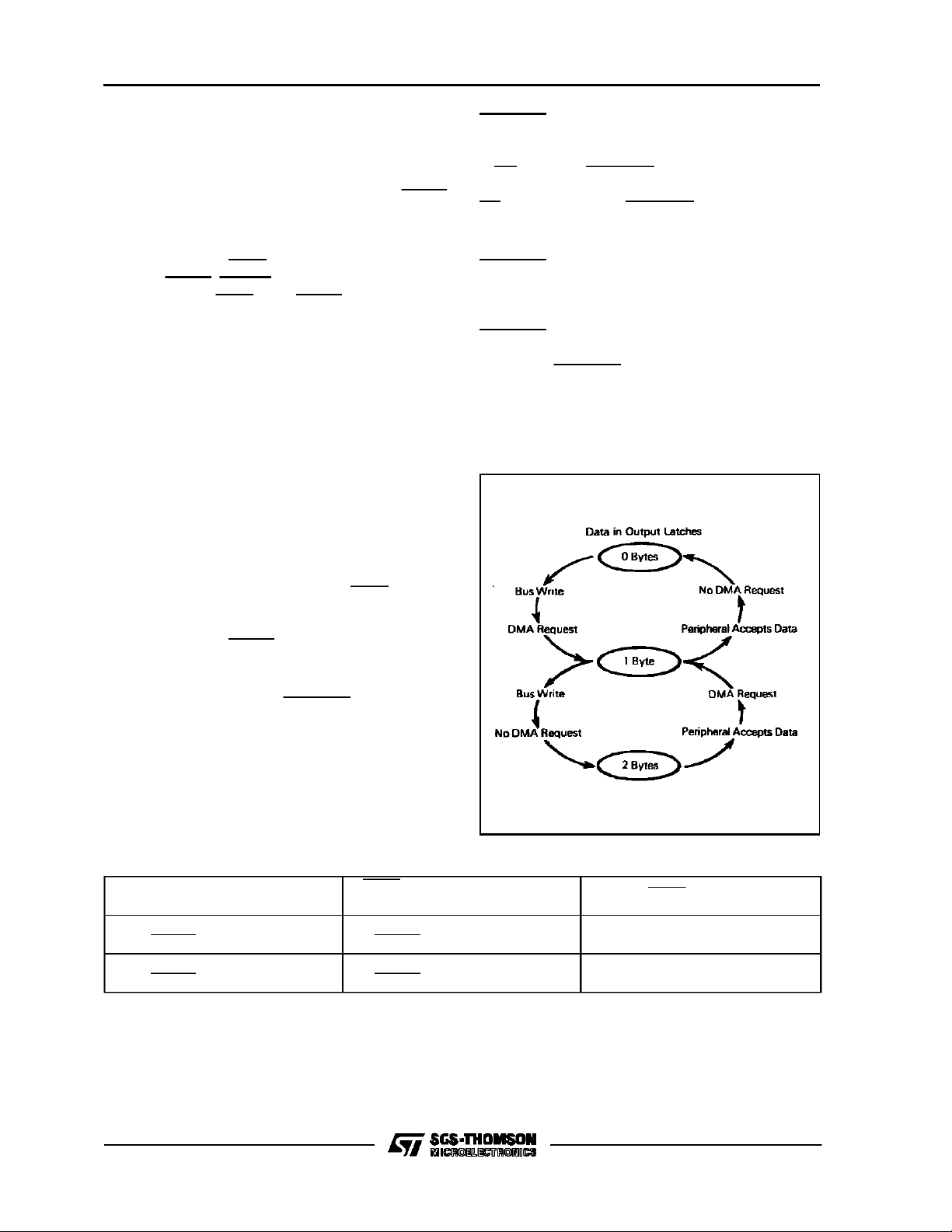
2.2.3. DMA REQUEST OPERATION. The direct
memory access request (DMAREQ) pulse (when
enabled) isassociated withoutput or input transfers
tokeepthe initialand finaloutput latchesfullorinitial
and final input latches empty, respectively. Figures
2.3and 2.4showallthepossible pathsin generating
DMArequests. See4.2. Port ServiceRequest Re-
gister(PSRR)for programming the operationof the
DMA request bit.
DMAREQ is generated on the bus side of the
TS68230 by the synchronized* chip select. If the
conditionsof figures2.3or 2.4aremet, anassertion
ofCS willcauseDMAREQ tobeassertedthreePI/T
clocks(plusthedelay timefromthe clockedge)after
CS is synchronized. DMAREQ remains asserted
threeclockcycles(plusthedelaytimefromtheclock
edge) andis then negated.
DMAREQ pulses are associated with peripheral
transfers or are generated by the synchronized*
H1(H3) input. If the conditions of figures2.3 or 2.4
aremet, an assertion of theH1(H3) input will cause
DMAREQ to be asserted 2.5PI/T clock cycles(plus
the delaytime fromclockedge) afterH1(H3)is synchronized. DMAREQ remains asserted threeclock
cycles(plus thedelaytimefrom the clockedge)and
is then negated.
Figure 2.3: DMAREQAssociated withOutput
Transfers.
Table 2.1 : Responseto Port InterruptAcknowledge.
Conditions
PIVR has not been initialized
since RESET.
PIVR has been initialized
since RESET.
PIR Q N egated OR Interrupt
Request Function not Selected
No Response from PI/T.
No DTACK.
No Response from PI/T.
No DTACK.
PIR Q Asserted
PI/T provides $0F, the Uninitialized
Vector*.
PI/T provides PIVR contents with
prioritization bits.
* The uninitialized vector is the value returned from an interrupt vector register before it has been initialized.
* Synchronized means that the appropriate input signal (H1, H3, or CS) has been sampled by the PI/T on the appropriatre
edge of the
clock (rising edge for H1(H3) and falling edge for CS). Refer to 1.4 BUS INTERFACE OPERATION for the exception concer-
16/61

TS68230
Figure 2.4 : DMAREQ Associated with Input
Transfers.
V000313
2.3. DIRECT METHODOF RESETTING STATUS
In certain modes one or more handshake pins can
be used as edge-sensitive inputs for the sole purposeof settingbits intheport statusregister. These
bitsconsistof simpleflip-flops.Theyareset (toone)
by the occurrence of the asserted edge of the
handshake pin input.Resetting ahandshake status
bit can be done by writingan 8-bitmask to the port
statusregister.Thisiscalledthedirect methodofresetting.To reseta statusbit that is resettable by the
direct method, the mask must contain a onein the
bitposition of theportstatus register corresponding
to the desired status bit. For statusbits that are not
resettableby thedirectmethodin thechosen mode,
the datawrittento the portstatus register hasno effect. For status bitsthat are resettable by thedirect
methodinthe chosen mode, a zeroin themaskhas
no effect.
2.4. HANDSHAKE PIN SENSECONTROL
The PI/Tcontains exclusive-OR gates tocontrol the
sense of eachof the handshakepins,whetherused
as inputs or outputs. Four bits in the port general
control register may be programmed to determine
whether the pins are asserted in the low- or highvoltage state.As with other controlregisters, these
bits arereset tozero whenthe RESET pin is asserted, defaulting the asserted level to be low.
2.5. ENABLING PORTS A ANDB
Certain functions involved with double-buffered da-
ta transfers, thehandshake pins, andthe statusbits
may be disabled by the external system or by the
programmer during initialization. The port general
control register contains two bits, H12 enable and
H34 enable, which control these functions. These
bits are cleared to the zero state when the RESET
pin isasserted, and the functions are disabled. The
functionsare the following :
1.Independent of other actions by the bus master or peripheral (viathe handshake pins), the
PI/T’s disabledhandshakecontroller is held to
the ”empty”state; i.e.,no dataispresent inthe
double-buffered data path.
2.When any handshake pinis used toset a simple status flip-flop, unrelated to double-buffered transfers, theseflip-flops are heldreset to
zero (seetable 1.1).
3.When H2(H4) is used in an interlocked or pulsed handshake with H1(H3), H2(H4) is held
negated,regardless ofthe chosenmode,submode,and primary direction. Thus,fordoublebuffered input transfers,the programmer may
signal a peripheral when the PI/T is ready to
begin transfers by setting the associated
handshake enable bit to one.
2.6. PORT A ANDB ALTERNATE REGISTERS
Inaddition totheportAandBdataregisters, thePI/T
contains port A and B alternate registers. These registersarereadonly,andsimplyprovide the ins-tantaneous (non-latched) level of each port pin. They
have no effect on the operation of the hand-shake
pins,double-buffered transfers,statusbits,or anyother aspect ofthePI/T,andtheyaremode/submode
independent. Refer to 4.7. Port Alternate Regis-
ters for further information.
17/61

TS68230
SECT IO N 3
PORT MODES
This sectioncontains information that distinguishes
the various port modes and submodes. General
characteristics common to allmodes are definedin
Section 2Port GeneralInformationand Conventions. A description of the port A control register
(PACR) and port Bcontrol register (PBCR)is given
beforeeach modedescription. Aftereach submode
description,the programmable options arelistedfor
that submode.
3.1. PORT A CONTROLREGISTER (PACR)
7 6543 2 1 0
Port A
Submode
H2 Control
H2
Interrupt
Enable
H1
SVCRQ
Enable
H1
Status
Control
The port A control register, in conjunction with the
programmed mode and the port B submode,
controls the operation of port A and the handshake
pinsH1and H2. TheportA control register contains
fivefields : bits7 and 6 specifythe port Asubmode;
bits5, 4, and3controlthe operation oftheH2 handshake pin and the H2S status bit ; bit 2 determines
whetheraninterrupt willbegenerated whentheH2S
statusbitgoes toone ; andbit1 determines whether
aservicerequest (interrupt requestorDMArequest)
willoccur;bit0controls theoperationof theH1Sstatus bit. The PACR is always readable andwritable.
All bits are cleared to zero when the RESET pin is
asserted.When theport Asubmodefieldisrelevant
ina mode/submode definition,it must notbealtered
unless the H12enable bitin theportgeneral control
register is clear (seetable 1.3 located at theend of
this document). Altering these bits will give unpredictable results.
3.2. PORT B CONTROLREGISTER (PBCR)
7 6543 2 1 0
Port B
Submode
H4 Control
H4
Interrupt
Enable
H3
SVCRQ
Enable
H3
Status
Control
Theport Bcontrolregister specifies theoperation of
port Band the handshakepins H3and H4. Theport
B control register contains five fields : bits 7 and 6
specifythe portB submode ; bits5, 4,and 3 control
theoperation ofthe H4handshake pin and H4Sstatus bit; bit 2 determines whetheran interrupt willbe
generated when the H4S status bit goes to a one ;
bit1determines whethera servicerequest (interrupt
request or DMA request) will occur ; and bit 0
controls the operation of the H3S status bit. The
PBCRis alwaysreadable and writable. There isnever a consequence to reading the register.
All bits are cleared to zero when the RESET pin is
asserted. WhentheportB submodefieldisrelevant
ina mode/submode definition, itmustnot bealtered
unlessthe H34enable bit in theport general control
register is clear (see table 1.3 located at the end of
thisdocument).
3.3.MODE 0 - UNIDIRECTIONAL 8-BIT MODE
In mode 0, ports A and B operate independently.
Eachmay beconfigured inany of its three possible
submodes :
Submode 00-Pin-Definable Double-Buffered Input orSingle-Buffered Output
Submode 01 - Pin-Definable Double-Buffered
Output orNon-Latched Input
Submode 1X- Bit I/O(Pin-Definable Single-Buffered Output or Non-Latched Input)
Handshake pinsH1and H2 areassociatedwithport
A andconfigured by programming theportA control
register. (The H12 enable bit of the port general
control register enables port A transfers). Handshake pins H3 and H4 are associated with port B
and configured by programming the port B control
register. (The H34 enable bit of the port general
control register enables port B transfers).The port
A and B data direction registers operate in all three
submodes. Alongwith the submode, theyaffect the
data read andwrite at the associated data register
according to table3.1. They also enable the output
buffer associated with each portpin. TheDMAREQ
pin may be associated with either (not both) port A
orportB,butdoesnotfunctionifthebitI/Osubmode
(submode 1X) is programmed for the chosen port.
18/61

Table 3.1 : Mode 0 Port Data Paths.
TS68230
Mode
0 Submode 00
0 Submode 01
0 Submode 1X
Abbreviations :
IOL - Initial Output Latch
FOL - Final Output Latch
FIL - Final Input Latch
Note 1 : Data is latched in the output data registers (final output latch) and will be single buffered at the pin if
the DDR is 1. The output buffers will be turned off if the DDR is 0.
Note 2 : Data is latched in the double-buffered output data registers. The data in the final output latch will
appear on the port pin if the DDR is a 1.
Note 3 : The output drivers that connect the final output latch to the pins are turned on
3.3.1.SUBMODE 00 - PIN-DEFINABLE DOUBLE-
BUFFERED INPUT OR SINGLE-BUFFERED
OUTPUT. In mode 0, double-buffered input transfersof up toeightbits areavailable by programming
submode 00 in the desired port’s control register.
Datathat meets theport setupand holdtimesis latchedon the asserted edge of H1(H3)and isplaced
in the initial or finalinput latch. H1(H3)is edge sensitive and may assume any duty cycle as long as
bothhighandlowminimumtimesareobserved. The
PI/Tcontainsa portstatusregisterwhoseH1S(H3S)
status bit is set anytime anyinput data thathas not
been read by thebus masteris present in the double-buffered latches. The action of H2(H4) is programmable. The following options are available :
1. H2(H4) maybe an edge-sensitive status input
thatis independent of H1(H3) and the transfer
of port data. On the assertededge of H2(H4),
the H2S(H4S) status bit isset. It is cleared by
eithertheRESETpin being asserted,writinga
oneto theparticular statusbit inthe portstatus
register (PSR), or when the H12enable (H34
enable) bit of the port general register is clear.
2. H2(H4) may be a general-purpose output pin
that is always negated. In this case the
H2S(H4S) status bit is always clear.
3. H2(H4) may be a general-purpose output pin
that is always asserted. In this case the
H2S(H4S) status bit is always clear.
4. H2(H4)maybe anoutput pinin theinterlocked
inputhandshake protocol. It is assertedwhen
the port input latches are ready to acceptnew
data. It is negated asynchronously following
Read P ort A/B Data Register Write Port A/B Data Register
DDR = 0 DDR = 1 DDR = X
FIL, D. B.
Pin
Pin
FOL Note 3
FOL Note 3
FOL Note 3
S. B. - Single Buffered
D. B. - Double Buffered
DDR - Data Direction Register
FOL, S. B.
IOL/FOL, D. B.
FOL, S. B.
Note 1
Note 2
Note 1
as the input latches become ready, H2(H4) is
again asserted. When the inputdouble-buffered latches are full, H2(H4) remains negated
until data is removed. Thus, anytime the
H2(H4) outputisasserted, new inputdatamay
be entered by asserting H1(H3). At other
times, transitions on H1(H3) are ignored. The
H2S(H4S) status bit is always clear. When
H12 enable (H34 enable) in the port general
controlregister is clear, H2(H4) is held negated.
5. H2(H4) may be an output pin in the pulsedinput handshake protocol. It is asserted exactly
as in the interlockedinput protocol above, but
neverremains assertedlongerthan fourclock
cycles.Typically, afourclockcyclepulseis generated. But in the case of a subsequent
H1(H3) asserted edge occurring beforetermination of the pulse, H2(H4) is negated asynchronously. Thus, anytime after the leading
edge of the H2(H4) pulse, new data may be
entered in the double-buffered input latches.
TheH2S(H4S)statusbitisalwaysclear.When
H12 enable (H34 enable) is clear, H2(H4) is
heldnegated.
For pins used as outputs,the datapath consists of
a singlelatch driving the output buffer.Data written
to the port’s data register does not affectthe operationof any handshake pin or status bit. Output pins
may be used independently of the input transfers.
However, readbus cyclesto thedata register do remove datafrom theport. Therefore, care should be
taken to avoid processor instructions that perform
unwanted read cycles.
theassertededgeoftheH1(H3)input. Assoon
19/61

TS68230
Programmable Options Mode 0 - Port A Submode 00 and Port B Submode00
PACR
7 6 PortA Submode
0 0 Submode 00
PACR
5 4 3 H2 Control
0 XX Input pin - edge-sensitive statusinput, H2Sis set on an asserted edge.
1 0 0 Outputpin - negated, H2S is always clear.
1 0 1 Outputpin - asserted,H2S is always clear.
1 1 0 Outputpin - interlocked input handshake protocol, H2S is always clear.
1 1 1 Outputpin - pulsed inputhandshake protocol, H2Sis alwaysclear.
PACR
2 H2 InterruptEnable
0 The H2 interrupt is disabled.
1 The H2 interrupt is enabled.
PACR
1 H1 SVCR Enable
0 The H1 interrupt and DMA request are disabled.
1 The H1 interrupt and DMA request are enabled.
PACR
0 H1 StatusControl
X The H1S status bit is setanytime input data is present in thedouble-buffered input path.
PBCR
7 6 PortB Submode
0 0 Submode 00
PBCR
5 4 3 H4 Control
0 XX Input pin - edge-sensitive statusinput, H4Sis set on an asserted edge.
1 0 0 Outputpin - negated, H4S is always cleared.
1 0 1 Outputpin - asserted,H4S is always cleared.
1 1 0 Outputpin - interlocked input handshake protocol, H4S is always cleared.
1 1 1 Outputpin - pulsed inputhandshake protocol,H4S is alwayscleared.
20/61

Programmable Options Mode 0 - Port A Submode 00 and Port B Submode00 (continued)
PBCR
2 H4 InterruptEnable
0 The H4 interrupt is disabled.
1 The H4 interrupt is enabled.
PBCR
1 H3 SVCRQEnable
0 The H3 interrupt and DMA request are disabled.
1 The H3 interrupt and DMA request are enabled.
PBCR
0 H3 StatusControl
X The H3S status bit is setanytime input data is present in thedouble-buffered input path.
TS68230
3.3.2.SUBMODE 01 - PIN-DEFINABLE DOUBLEBUFFEREDOUTPUTORNON-LATCHED INPUT.
In mode0, double-buffered outputtransfers ofup to
eight bits are available by programming submode
01 inthe desired port’s control register. The operation ofH2 andH4 may beselectedby programming
the port A and B control registers, respectively. Data, writtenby thebus master to thePI/T, is storedin
theport’soutput latches. Theperipheral acceptsthe
databyassertingH1(H3),whichcausesthenext data to be movedto theport’s output latchas soon as
it is available.
The H1S(H3S) status bit may be programmed for
two interpretations :
1. The H1S(H3S) statusbitisset wheneitherthe
port initial or final output latchcan accept new
data. It is cleared when both latches are full
and cannot acceptnew data.
2. The H1S(H3S) status bit is set when both of
the port output latches are empty.It is cleared
whenat leastone latchis full.
The programmable options of the H2(H4)pin are :
1. H2(H4) maybe an edge-sensitive input pin independent of H1(H3) and the transfer of port
data. On the asserted edge of H2(H4), the
H2S(H4S) status bit is set. It is cleared by either the RESET pin being asserted, writing a
oneto theparticular statusbit inthe portstatus
register (PSR), or when the H1(H2) enable
(H3(H4) enable) bit of the portgeneralcontrol
register is clear.
2. H2(H4) may be a general-purpose output pin
that is always negated. The H2S(H4S) status
bit is always clear.
3. H2(H4) may be a general-purpose output pin
thatis always asserted. The H2S(H4S)status
bit is always clear.
4. H2(H4)maybe anoutputpinintheinterlocked
output handshake protocol. H2(H4) is assertedtwo clockcyclesafterdata istransferred to
the double-buffered output latches. The data
remains stable at the portpins and H2(H4) remainsasserteduntilthenext assertededge of
the H1(H3) input. At that time,H2(H4) is asynchronously negated. As soon asthe next data
is available, it is transferred to the output
latches. When H2(H4) is negated, asserted
transitions of H1(H3) have no affect on data
paths.TheH2S(H4S)statusbitisalwaysclear.
When H12 enable (H34 enable) is clear,
H2(H4) is held negated.
5. H2(H4)maybe anoutput pininthe pulsedoutput handshake protocol. It is asserted exactly
as inthe interlocked protocolabove, butnever
remains asserted longer than four clock cycles.Typically, a fourclockpulseisgenerated.
But in the casethat a subsequentH1(H3) asserted edge occurs before termination of the
pulse, H2(H4) is negated asynchronously
shorteningthe pulse.The H3S(H4S) statusbit
is always clear. When H12 enable (H34
enable) isclear H2(H4) is held negated.
For pins used asinputs,data writtento theassociated data register is double-buffered and passed to
the initial orfinal output latch, but, the output buffer
is disabled.
21/61

TS68230
Programmable Options Mode 0 - Port A Submode 01 and Port B Submode01
PACR
7 6 PortA Submode
0 1 Submode 01
PACR
5 4 3 H2 Control
0 XX Input pin - edge-sensitive statusinputs, H2S isset onan assertededge.
1 0 0 Outputpin - negated, H2S is always clear.
1 0 1 Outputpin - asserted,H2S is always clear.
1 1 0 Outputpin - interlocked input handshake protocol, H2S is always clear.
1 1 1 Outputpin - pulsed inputhandshake protocol,H2S is alwaysclear.
PACR
2 H2 InterruptEnable
0 The H2 interrupt is disabled.
1 The H2 interrupt is enabled.
PACR
1 H1 SVCRQEnable
0 The H1 interrupt and DMA request are disabled.
1 The H1 interrupt and DMA request are enabled.
PACR
0 H1 StatusControl
0 The H1S status bit is setwhen either the portA initial or final output latch can accept new data
It is clear when both latches are fulland cannot accept new data.
1 The H1S status bit is one when both ofthe port A output latches are empty.It is clear when at
least one latchis full.
PBCR
7 6 PortB Submode
0 1 Submode 01
PBCR
5 4 3 H4 Control
0 XX Input pin - edge-sensitive statusinput, H4Sis set on an asserted edge.
1 0 0 Outputpin - negated, H4S is always cleared.
1 0 1 Outputpin - asserted,H4S is always cleared.
1 1 0 Outputpin - interlocked input handshake protocol, H4S is always cleared.
1 1 1 Outputpin - pulsed inputhandshake protocol,H4S is alwayscleared.
22/61

TS68230
Programmable Options Mode 0 - Port A Submode 01 and Port B Submode01 (continued)
PBCR
2 H4 InterruptEnable
0 The H4 interrupt is disabled.
1 The H4 interrupt is enabled.
PBCR
1 H3 SVCRQEnable
0 The H3 interrupt and DMA request are disabled.
1 The H3 interrupt and DMA request are enabled.
PBCR
0 H3 StatusControl
0 The H3S status bit is setwhen either the portB initial or final output latch can accept new data.
It is clear when both latches are fulland cannot accept new data.
1 The H3S status bit is one when both ofthe port B output latches are empty.It is clear when at
least one latchis full.
3.3.3. SUBMODE 1X - BIT I/O (PIN-DEFINABLE
SINGLE-BUFFERED OUTPUT OR NON-LATCHEDINPUT). In mode0,simplebit I/Oisavailable
by programming submode 1X in the desired port’s
controlregister. This submode is intended forapplications in whichseveral independent devices must
be controlled or monitored. Data written to the associated(input/output) register is single buffered. If
the data direction register bit for that pin is a one
(output), the output buffer is enabled. If it is a zero
(input)data writtenisstilllatched,butis notavailable
at the pin.Data readfrom the data register is the instantaneous valueof the pin or what was written to
the data register, depending on the contents of the
data direction register. H1(H3) is an edge-sensitive
status input pin only and it controls no data related
function.TheH1S(H3S)statusbitissetfollowing the
assertededgeof theinput waveform. Itiscleared by
eitherthe RESET pin being asserted,writing a one
tothe associated statusbit intheportstatusregister
(PSR),or whenthe H12enable (H34 enable) bit of
the port general control register isclear. H2 maybe
programmed as :
1. H2(H4) may bean edge-sensitive status input
thatis independent of H1(H3) and the transfer
of port data. On the asserted edgeof H2(H4),
the H2S(H4S) status bit is set.It iscleared by
either the RESETpinbeing asserted, writinga
oneto theparticularstatusbitin theportstatus
register (PSR), or whenthe H12 enable(H34
enable) bit of the port general control register
is clear.
2. H2(H4) may be a general-purpose output pin
that is always negated. In this case the
H2S(H4S) status bit is always clear.
3. H2(H4) may be a general-purpose output pin
that is always asserted. In this case the
H2S(H4S) status bit is always clear.
23/61

TS68230
Programmable OptionMode 0 - Port A Submode 1X and Port B Submode 1X
PACR
7 6 PortA Submode
1 X Submode 1X
PACR
5 4 3 H2 Control
0 XX Input pin - edge-sensitive statusinput, H2Sis set on an asserted edge.
1 X0 Output pin -negated, H2S is always cleared.
1 X1 Output pin -asserted, H2S is always cleared.
PACR
2 H2 InterruptEnable
0 The H2 interrupt is disabled.
1 The H2 interrupt is enabled.
PACR
1 H1 SVCRQEnable
0 The H1 interrupt is disabled.
1 The H1 interrupt is enabled.
PACR
0 H1 StatusControl
X H1 isan edge-sensitive status input, H1S is set by an assertededge of H1.
PBCR
7 6 PortB Submode
1 X Submode 1X.
PBCR
5 4 3 H4 Control
0 XX Input pin - edge-sensitive statusinput, H4Sis set on an asserted edge.
1 X0 Output pin -negated, H4S is always cleared.
1 X1 Output pin -asserted, H4S is always cleared.
PBCR
2 H4 InterruptEnable
0 The H4 interrupt is disabled.
1 The H4 interrupt is enabled.
PBCR
1 H3 SVCRQEnable
0 The H3 interrupt is disabled.
1 The H3 interrupt is enabled.
24/61

Programmable Options Mode 0 - Port A Submode 1X and Port B Submode 1X (continued)
PBCR
0 H3 StatusControl
X H3 isan edge-sensitive status input, H3S is set by an assertededge of H3.
TS68230
3.4. MODE 1 - UNIDIRECTIONAL16-BIT MODE
In mode 1,ports A and B are concatenated to form
a single 16-bit port. The port B submode field
controlstheconfiguration ofbothports.Thepossible
submodes are :
Port B Submode X0 - Pin-Definable Double-Buffered Input or Single-Buffered Output
Port B Submode X1 - Pin-Definable Double-Buffered Output or Non-Latched Input
HandshakepinsH3and H4,configured byprogrammingthe port B control register, are associated with
the 16-bit double-buffered transfer. These 16-bit
transfersare enabled by settingthe H34 enable bit
in the port general control register (PGCR). HandshakepinsH1 andH2may beusedas simplestatus
inputs not related to the 16-bit data transfer or H2
maybeanoutput.Enabling ofthe H1andH2handshake pins is done by setting the H12 enable bit of
the port general control register. The port A and B
data direction registers operate in each submode.
Along with the submode, they affect the data read
and written at the data register according to table
3.2.Thedatadirection register alsoenables theoutput buffer associated with each port pin. The DMAREQpin may be associatedonly withH3.
Table 3.2 : Mode 1 Port Data Paths.
Mode
1, Port B
Submode X0
1, Port B
Submode X1
Note 1 : Data written to Port A goes to a temporary latch. When the Port B data register is later written, Port A
data is transferred to IOL/FOL.
Note 2 : Data is latched in the output data registers (final output latch) and will be single buffered at the pin if
the DDR is 1. The output buffers will be turned off if the DDR is 0.
Note 3 : The output drivers that connect the final output latch to the pins are turned on.
Abbreviations :
IOL - Initial Output Latch
FOL - Final Output Latch
FIL - Final Input Latch
Re a d Port A/B R eg i ster Writ e Port A/B Re g ister
DDR = 0 DDR = 1 DDR = 0 DDR = 1
FIL, D. B.
Pin
FOL
Note 3
FOL
Note 3
S. B. - Single Buffered
D. B. - Double Buffered
DDR - Data Direction Register
FOL, S. B.
Note 2
IOL/FOL, D. B.
Note 1
FOL, S. B.
Note 2
IOL/FOL, D. B.
Note 1
Mode 1 can provide convenient high-speed 16-bit
transfers. The port A and port B data registers are
addressed forcompatibility withthe TS68000 move
peripheral (MOVEP) instruction and with the 68440
direct memory access controller (DMAC). To take
advantage of this, port A should contain the mostsignificant byteof dataandalwaysbereadorwritten
by the bus master first. The interlocked and pulsed
handshake protocols, statusbits,andDMAREQare
keyed to theaccess of port B data register in mode
1. Transfers proceed properly with interlocked or
pulsedhandshakes whenthe port B dataregister is
accessedlast.
25/61

TS68230
3.4.1.PORT A CONTROLREGISTER(PACR).
765432 1 0
Port A
Submode H2 Control
H2
Interrupt
Enable
H1
SVCRQ
Enable
H1
Status
Control
The port A control register, in conjunction with the
programmed mode and the port B submode,
controls the operation of port A and the handshake
pinsH1and H2. TheportA control register contains
fivefields : bits7 and 6 specifythe port Asubmode;
bits5, 4, and3controlthe operation oftheH2 handshakepinand H2Sstatusbit; bit2 determines whether an interrupt will be generated when the H2S
status bit goes to one ; bit 1 determines whether a
servicerequest (interrupt request or DMA request)
willoccur;andbit0controls theoperation oftheH1S
status bit. The PACR is always readable andwritable.There isnevera consequenceto reading theregister.
Allbitsarecleared tozerowhentheRESETpinis asserted.When the port Asubmode fieldis relevant in
amode/submodedefinition,itmustnotbealtered unlesstheH12 enable bitin the portgeneral controlregisterisclear(see table 1.3 located at theend ofthis
document). Altering these bits may give unpredictable results if the H12 enable bit in the PGCRis
set.
3.4.2.PORT B CONTROLREGISTER(PBCR).
7 6543 2 1 0
Port B
Submode H4Control
H4
Interrupt
Enable
H3
SVCRQ
Enable
H3
Status
Control
The port Bcontrolregister specifies the operation of
portB and thehandshake pins H3and H4.The port
B control register contains five fields : bits 7 and 6
specifythe port B submode ; bits 5, 4, and 3control
theoperation oftheH4handshake pinandH4S statusbitgoesto aone;bit1determines whether aservicerequest (interrupt request or DMA request) will
occur ; and bit 0 controls the operation of the H3S
status bit. The PBCR is always readable andwritable.
All bits are cleared to zero when the RESET pin is
asserted.When theport Bsubmodefieldisrelevant
ina mode/submode definition,it must notbealtered
unless the H34enable bitin theportgeneral control
register is clear (seetable 1.3 located at theend of
thisdocument). Altering these bitsmay give unpredictableresultsif the H12 enablebit inthe PGCRis
set.
3.4.3.SUBMODE X0- PIN-DEFINABLE DOUBLEBUFFERED INPUT OR SINGLE-BUFFERED
OUTPUT.In mode 1 submodeX0, double-buffered
inputtransfers ofupto 16 bitsmaybeobtained.The
level of each pin is asynchronously latched withthe
asserted edge of H3 and placed in the initial input
latch or the final input latch. The processor may
checkthe H3S status bitto determine ifnew data is
present. The DMAREQ pin maybe used to signala
DMA controller to empty the input buffers. Regardlessof the bus master, portA data shouldbe read
first and port B data should be read last. The operationof theinternal handshake controller, theH3S
bit,and theDMAREQarekeyedtothereadingofthe
port Bdata register. (The 68440DMAC canbe programmed toperform theexact transfersneeded for
compatibilitywiththePI/T.)H4maybeprogrammed
as :
1. H4 may be an edge-sensitive status inputthat
is independent of H3 and the transfer of port
data.OntheassertededgeofH4,theH4Sstatus bit is set. It is cleared by either theRESET
pin being asserted, writinga one to the particular statusbitintheportstatusregister(PSR),
or whenthe H34enable bit of the port general
controlregister is clear.
2. H4 may be a general-purpose output pin that
is always negated. In thiscase the H4Sstatus
bit is always clear.
3. H4 may be a general-purpose output pin that
is always asserted.In thiscasetheH4S status
bit is always clear.
4. H4 maybe an output pin in the interlocked input handshake protocol. It is asserted when
the port inputlatches are ready to accept new
data. It is negated asynchronously following
the asserted edge of the H3 input.As soon as
the input latches become ready, H4 is again
asserted. When the input double-buffered
latchesare full,H4 remainsnegated until data
isremoved.Thus,anytime theH4 output isasserted,new input data may be entered by asserting H3.Atothertimestransitionson H3are
ignored. The H4S status bit is always clear.
When H34 enable in the port general control
register is clear, H4is heldnegated.
26/61

TS68230
5. H4 may be an output pin in the pulsed input
handshake protocol. It isasserted exactlyas in
the interlocked input protocolabove,but never
remainsasserted longer thanfourclockcycles.
Typically, afourclockcyclepulseis generated.
But inthe case that a subsequent H3 asserted
edgeoccursbeforeterminationofthepulse,H4
isnegatedasynchronously. Thus,anytimeafter
theleadingedgeoftheH4pulse,newdatamay
beenteredinthedouble-buffered inputlatches.
The H4Sstatus bit is alwaysclear.When H34
enable isclear, H4 is held negated.
For pins used as outputs,the datapath consists of
a singlelatch driving the output buffer. Data written
to the port’s data register does notaffectthe operationofanyhandshake pin, statusbit,oranyotheraspect of the PI/T. Thus, output pins may be used
independently of theinput transfer.
Programmable Options Mode 1 - Port A Submode XX and Port B SubmodeX0
PACR
7 6 PortA Submode
0 0 Submode XX
The programmable options of the H2 pin are:
1. H2 may be an edge-sensitive input pin independent ofH1and thetransferof port data. On
the assertededge of H2, the H2S statusbit is
set.It iscleared byeithertheRESETpinbeing
asserted, writing a oneto the particularstatus
bitin theportstatusregister (PSR),orwhenthe
H12 enable bit of the port general control registeris clear.
2. H2 may be a general-purpose output pin that
is always negated. The H2S status bit is alwaysclear.
3. H2 may be a general-purpose output pin that
is always asserted. The H2S status bit is alwaysclear.
PACR
5 4 3 H2 Control
0 XX Input pin - edge-sensitive statusinput, H2Sis set on an asserted edge.
1 X0 Output pin -negated, H2S is always cleared.
1 X1 Output pin -asserted, H2S is always cleared.
PACR
2 H2 InterruptEnable
0 The H2 interrupt is disabled.
1 The H2 interrupt is enabled.
PACR
1 H1 SVCRQEnable
0 The H1 interrupt is disabled.
1 TheH1 interrupt is enabled.
PACR
0 H1 StatusControl.
X H1 isan edge-sensitive status input. H1S is set by an assertededge of H1.
PBCR
7 6 PortB Submode
0 0 Submode X0.
27/61

TS68230
Programmable Options Mode 1 - Port A Submode XX and Port B SubmodeX0 (continued)
PBCR
5 4 3 H4 Control
0 XX Input pin - edge-sensitive statusinput, H4Sis set on an asserted edge.
1 0 0 Outputpin - negated, H4S is always cleared.
1 0 1 Outputpin - asserted, H4S is always cleared.
1 1 0 Outputpin - interlocked input handshake protocol.
1 1 1 Outputpin - pulsed inputhandshake protocol.
PBCR
2 H2 InterruptEnable
0 The H4 interrupt is disabled.
1 The H4 interrupt is enabled.
PBCR
1 H3 SVCRQEnable
0 The H3 interrupt and DMA request are disabled.
1 The H3 interrupt and DMA request are enabled.
PBCR
0 H3 StatusControl
X The H3S status bit is setanytime input data is present in thedouble-buffered input path.
3.4.4.SUBMODE X1- PIN-DEFINABLE DOUBLEBUFFEREDOUTPUTORNON-LATCHED INPUT.
In mode 1 submode X1, double-buffered output
transfers of up to 16 bits may be obtained. Data is
written by the bus master (processor or DMA controller)in two bytes. The firstbyte (mostsignificant)
is written to the port A data register. It is storedin a
temporary latch until the next byte is written to the
portB dataregister.Then all 16 bits aretransferred
to one of the output latches of ports A and B. The
DMAREQpin maybeused tosignala DMAcontroller to transfer another word to the port output
latches. (The 68440 DMAC can be programmed to
perform the exacttransfers needed forcompatibility
withthe PI/T.)H4 may be programmed as :
1. H4 may be an edge-sensitive status input that
is independent of H3 and the transfer of port
data.OntheassertededgeofH4, theH4Sstatus bit is set. It iscleared by eitherthe RESET
pin being asserted, writing a one to the particularstatusbitinthe portstatusregister(PSR),
or whenthe H34 enable bitof the port general
controlregister is clear.
2. H4 may be a general-purpose output pin that
is always negated. In this casethe H4Sstatus
bit is always clear.
3. H4 may be a general-purpose output pin that
is always asserted.In thiscasetheH4S status
bit is always clear.
4. H4 maybe anoutput pininthe interlocked output handshake protocol. H4 is asserted two
clockcyclesafterdatais transferredtothedouble-buffered output latches. Thedata remains
stable at the port pins and H4 remains asserteduntilthenext assertededgeof theH3 input.
Atthattime,H4isasynchronously negated. As
soon as the next data is available, it is transferredto the output latches.WhenH4 is negated, asserted transitions of H3 have no affect
on data paths. The H4S status bit is always
clear. WhenH34enableis clear, H4is heldnegated.
5. H4 maybe an output pinin the pulsed output
handshake protocol. Itis assertedexactlyasin
the interlocked protocol above, but never remains asserted longer than four clock cycles.
Typically, a four clock pulse is generated. But
in the case that a subsequent H3 asserted
edge occurs before termination of the pulse,
H4 is negated asynchronously shortening the
pulse. The H4S status bit is always cleared.
WhenH34enable isclear,H4 is heldnegated.
28/61

TS68230
The H3S statusbit may be programmed for two interpretations :
1. The H3S statusbit is set when either the port
initialor finaloutput latchcan acceptnewdata.
Itis clearwhenbothlatchesarefulland cannot
accept new data.
2. The H3S statusbitis set whenboth of theport
output latches are empty. It is clear when at
least onelatch is full.
The programmable options of the H2 pinare :
1. H2 may be an edge-sensitive input pin independent ofH1and thetransferof portdata.On
the assertededge of H2, the H2S statusbit is
set.Itis clearedbyeitherthe RESET pinbeing
asserted, writing a one to theparticular status
Programmable Options Mode 1 - Port A Submode XX and Port B SubmodeX1
PACR
7 6 PortA Submode
0 0 Submode XX.
PACR
5 4 3 H2 Control
0 XX Input pin - edge-sensitive statusinput, H2Sis set on an asserted edge.
1 X0 Output pin -negated, H2S is always cleared.
1 X1 Output pin -asserted, H2S is always cleared.
bitin theportstatusregister (PSR),orwhenthe
H12 enable bit of the port general control registeris clear.
2. H2 may be a general-purpose output pin that
is always negated. The H2S status bit is alwaysclear.
3. H2 may be a general-purpose output pin that
is always asserted. The H2S status bit is alwaysclear.
For pins used as inputs, data written to either data
register is double buffered and passed to theinitial
or final output latch,as usual, but the output buffer
is disabled (refer to 3.3.2. Submode 01 - Pin-Defi-
nable Double-Buffered Output or Non-Latched
Input).
PACR
2 H2 InterruptEnable
0 The H2 interrupt is disabled.
1 The H2 interrupt is enabled.
PACR
1 H1 SVCRQEnable
0 The H1 interrupt is disabled.
1 The H1 interrupt is enabled.
PACR
0 H1 StatusControl
X H1 isan edge-sensitive status input. H1S is set by an assertededge of H1.
PBCR
7 6 PortB Submode
0 0 Submode X1.
29/61

TS68230
Programmable Options Mode 1 - Port A Submode XX and Port B SubmodeX1 (continued)
PBCR
5 4 3 H4 Control
0 XX Input pin - edge-sensitive statusinput, H4Sis set on an asserted edge.
1 0 0 Outputpin - negated, H4S is always cleared.
1 0 1 Outputpin - asserted,H4S is always cleared.
1 1 0 Outputpin - interlocked input handshake protocol.
1 1 1 Outputpin - pulsed inputhandshake protocol.
PBCR
2 H4 InterruptEnable
0 The H4 interrupt is disabled.
1 The H4 interrupt is enabled.
PBCR
1 H3 SVCRQEnable
0 The H3 interrupt and DMA request are disabled.
1 The H3 interrupt and DMA request are enabled.
PBCR
0 H3 StatusControl
0 The H3S status bit is setwhen either the initialor finaloutput latchof ports A and B can accept
new data. It isclear when both latches are fulland cannotaccept newdata.
1 The H3S status bit is setwhen boththe initial and final output latches of ports Aand B are empty.
The H3Sstatus bit is clearwhen at least one set of output latches is full.
3.5. MODE 2 - BIDIRECTIONAL8-BIT MODE
In mode2, port A isused for bit I/O with noassocia-
ted handshake pins. Port B is used for bidirectional
8-bitdouble-buffered transfers. H1andH2, enabled
by the H12 enable bit in the port general control register, control output transfers, while H3 and H4,
enabled bythe port general control register bit H34
enable, control input transfers. The instantaneous
direction of thedata is determined by the H1 handshake pin. The port B data direction register is not
used.The port A and port B submodefields do not
affectPI/T operation in mode2.
3.5.1.PORT A BIT I/O (PIN-DEFINABLE SINGLEBUFFERED OUTPUT OR NON-LATCHED IN-
PUT).Mode2,portA performssimple bitI/O withno
associated handshake pins.Thisconfiguration is intended for applications in which several independent devices must be controlled or monitored.
Data written to the port A data register issingle buffered. If theport Adata direction register bit for that
pin is set (output), the output buffer is enabled. If it
is zero (input), data written is still latched but not
available at thepin. Datareadfromthe dataregister
is either the instantaneous value of the pin (if data
isstablefrom CSassertedto DTACKasserted,data
on thesepinswillbeguaranteed validinthe dataregister)or what waswritten to the data register, depending on the contents ofthe port Adata direction
register. This is summarizedin table3.3.
30/61

Table 3.3 : Mode2 PortA DataPaths.
TS68230
Mode
2 Pin FOL FOL FOL, S. B.
Abbreviations :
S. B. - Single Buffered
FOL - Final Output Latch
DDR - Data Direction Register
Rea d Port A Da ta Reg ister Write Po rt A Data Register
DDR = 0 DDR = 1 DDR = 0 DDR = 1
3.5.2. PORT B - DOUBLE-BUFFERED BIDIRECTIONALDATA.TheoutputbuffersofportB arecontrolled by the level of H1. When H1 is negated, the
portB output buffers (alleight) are enabled and the
pinsdrivethe bidirectional bus. Generally, H1 is negated by the peripheral in response to an asserted
H2, whichindicates that new output data is present
in the double-buffered latches. Following acceptance of the data, the peripheral asserts H1, disablingtheportB outputbuffers.Otherthancontrolling
the output buffers, H1 is edge-sensitive as in other
modes.
3.5.2.1. Double-Buffered Input Transfers.
Port B input data that meetsthe port setupandhold
timesislatchedon theasserted edge of H3and placed intheinitial input latch orthe final input latch. H3
isedge-sensitive, andmayassumeanyduty-cycleas
longas both high andlowminimum timesare observed. The PI/T contains a portstatus register whose
H3S status bitis setanytime any input data that has
notbeen readbythebusmasterispresentinthedouble-bufferedlatches. Theactionof H4isprogrammable and can be programmed as :
1. H4 maybe an output pin in theinterlocked input handshake protocol. It is asserted when
the port input latches are ready to acceptnew
data. It is negated asynchronously following
the asserted edge of the H3 input. As soon as
the input latches become ready, H4 is again
asserted. When the input double-buffered
latchesare full,H4 remainsnegated untildata
is removed. Thus,anytimethe H4output isasserted, new input datamay be entered byassertingH3.At othertimestransitionsonH3are
ignored. The H4S status bit is always clear.
When H34 enable in the port general control
register is clear, H4 is heldnegated.
2. H4 may be an output pin in the pulsed input
handshake protocol. Itisassertedexactlyasin
theinterlocked inputprotocolabove,butnever
remains asserted longer than four clock cycles. Typically, a four clock cycle pulse is generated. But in the casethat a subsequent H3
assertededge occursbeforeterminationof the
pulse, H4 is negated asynchronously. Thus,
anytimeafter theleading edgeofthe H4pulse,
new datamay beentered in the double-buffered input latches. The H4Sstatusbit is always
clear. WhenH34enableis clear, H4is heldnegated.
3.5.2.2. Double-Buffered Output Transfers.
Data,writtenby thebusmaster tothe PI/T,isstored
inthe port’s outputlatch.Theperipheral acceptsthe
data byasserting H1,which causes the next datato
be moved to the port’s output latch as soon as it is
available. The H1S status bit, in the portstatus register,may be programmed for two interpretations.
Normally thestatus bitisaonewhenthere isatleast
one latch in the double-buffered data path that can
accept newdata.After writingonebyteof datatothe
ports,aninterrupt serviceroutine couldcheckthisbit
todetermine ifitcouldstoreanotherbyte ;thusfilling
both latches. When the bus master is finished, it is
oftenusefultobe ableto check whetherallof thedata has been transferred to the peripheral.The H1S
status control bit of the port A control register provides this flexibility. The H1S statusbit is set when
both output latches are empty. The programmable
optionsfor H2 are :
1. H2 maybe anoutput pininthe interlocked output handshake protocol. It is asserted when
the port output latches are ready to transfer
new data. It is negated asynchronously following the asserted edge of the H1 input. As
soon as the output latches become ready, H2
is again asserted. When the output doublebuffered latches are full,H2 remains asserted
until data is removed. Thus, anytime the H2
output is asserted, new output data may be
transferred by asserting H1. At other times
transitions onH1 are ignored. TheH2S status
bit is always clear. When H12 enable in the
portgeneral control register isclear,H2 isheld
negated.
2. H2 maybe an output pinin the pulsed output
handshake protocol. Itis assertedexactlyasin
the interlocked output protocol above, but neverremains assertedlongerthanfourclockcy-
31/61

TS68230
cles. Typically, a four clock cycle pulse is generated. But in the casethat a subsequent H1
assertededge occursbeforeterminationof the
pulse, H2 is negated asynchronously. Thus,
anytimeafterthe leadingedge ofthe H2pulse,
new data may be transferred to the doublebuffered output latches. The H2S status bit is
always clear. When H12enable isclear, H2 is
heldnegated.
TheDMAREQpin maybe associated with eitherinput transfers (H3) or output transfers (H1), but not
both. Referto table3.4 for a summaryof the port B
data register responses in mode 2.
Table 3.4 :Mode2 PortB DataPaths.
Mode Read Port B Data Register WritePortB Data Register
2 FIL, D. B. IOL/FOL, D. B.
Abbreviations :
IOL - Initial Output Latch
FOL - Final Output Latch
FIL - Final Input Latch
D. B. - Double Buffered
Programmable Options Mode 2 - Port A Submode XX and Port B SubmodeXX
PACR
7 6 PortA Submode
X X Submode XX.
PACR
5 4 3 H2 Control
X X 0 Output pin - interlocked outputhandshakeprotocol, H2S is always cleared.
X X 1 Output pin - pulsed outputhandshake protocol, H2S is always cleared.
PACR
2 H2 InterruptEnable
0 The H2 interrupt is disabled.
1 The H2 interrupt is enabled.
PACR
1 H1 SVCRQEnable
0 The H1 interrupt and DMA request are disabled.
1 The H1 interrupt and DMA request are enabled.
PACR
0 H1 StatusControl
0 The H1 status bit is set when eitherthe port B initialor final output latch canaccept new data. It
is clear when both latches are full and cannot accept new data.
1 The H1S status bit is setwhen bothof theport B output latchesare empty. Itis clear when at
least one latchis full.
PBCR
7 6 PortB Submode
X X Submode XX.
32/61

Programmable Options Mode 2 - Port A Submode XX and Port B SubmodeXX (continued)
PBCR
5 4 3 H4 Control
X X 0 Output pin - interlocked input handshake protocol, H4S isalways cleared.
X X 1 Output pin - pulsed input handshake protocol, H4S is alwayscleared.
PBCR
2 H4 InterruptEnable
0 The H4 interrupt is disabled.
1 The H4 interrupt is enabled.
PBCR
1 H3 SVCRQEnable
0 The H3 interrupt and DMA request are disabled.
1 The H3 interrupt and DMA request are enabled.
PBCR
0 H3 StatusControl
X The H3S status bit is setanytime input data is present in thedouble-buffered input path.
TS68230
3.6. MODE 3 - BIDIRECTIONAL16-BIT MODE
In mode 3, ports A andB are used for bidirectional
16-bitdouble-buffered transfers. H1 and H2 control
output transfers, while H3 and H4 control input
transfers. H1 and H2 are enabled by the H12 enable bitwhileH3and H4are enabledby theH34enable bit of the port general control register. The
instantaneous direction of dataisdetermined bythe
H1 handshake pin,thus, thedatadirection registers
arenot usedand havenoaffect.Theport Aandport
B submode fields do not affect PI/T operation in
mode 3. Port A and port B output buffers are controlled by the level of H1. When H1 is negated, the
outputbuffers(all16) areenabled and thepinsdrive
the bidirectional port bus.Generallya peripheralwill
negate H1in response to anassertedH2, whichindicates that new output data is present in the double-buffered latches. Following acceptance of the
data,theperipheral assertsH1,disabling theoutput
buffers.Other than controllingtheoutputbuffers,H1
is edge-sensitive as inother modes. The portA and
portB data direction registers are not used.
3.6.1.DOUBLE-BUFFERED INPUTTRANSFERS.
PortA andBinputdatathatmeetstheportsetupand
holdtimesislatched on the asserted edgeofH3and
placed in theinitialinputlatchor the finalinputlatch.
H3 isedge-sensitive, andmay assumeanyduty-cycle aslong asboth high andlow minimum timesare
observed. The PI/T contains a port status register
whoseH3S statusbit is set anytime any input data
ispresentinthedouble-buffered latchesthathasnot
been read by the bus master. The action of H4 is
programmable and can beprogrammed as :
1. H4 maybe an output pin in the interlocked input handshake protocol. It is asserted when
the port inputlatches are ready to accept new
data. It is negated asynchronously following
the asserted edge of the H3 input.As soon as
the input latches become ready, H4 is again
asserted. When the input double-buffered
latchesare full,H4 remainsnegated until data
isremoved.Thus,anytime theH4 output isasserted,new input data may be entered by asserting H3.Atothertimestransitionson H3are
ignored. The H4S status bit is always clear.
When H34 enable in the port general control
register is clear, H4is heldnegated.
2. H4 may be an output pin in the pulsed input
handshake protocol. It isasserted exactlyas in
theinterlocked input protocol above, but never
remains assertedlongerthanfourclockcycles.
Typically,afourclockcyclepulseisgenerated.
Butin the case that a subsequent H3 asserted
edgeoccursbeforeterminationof thepulse, H4
isnegatedasynchronously. Thus,anytimeafter
theleading edge oftheH4pulse,newdatamay
beentered inthedouble-buffered inputlatches.
TheH4statusbitisalwaysclear.When H34enable is clear,H4 is held negated.
33/61

TS68230
3.6.2. DOUBLE-BUFFERED OUTPUT TRANSFERS. Data, written by the bus master to the PI/T,
isstoredin theport’soutput latch.The peripheralaccepts the data by asserting H1, which causes the
next data to be movedto the port’s output latch as
soonas itisavailable. TheH1Sstatusbit, intheport
status register, may be programmed for two interpretations. Normally the status bit is a one when
thereisat leastonelatchinthedouble-buffered data
paththatcanacceptnewdata.Afterwritingonebyte
ofdatatotheports,aninterrupt serviceroutine could
check this bit to determine if it could store another
byte; thus filling both latches.When thebusmaster
is finished,itis oftenusefulto beableto checkwhetherall of thedata hasbeen transferred tothe peripheral. The H1S status control bit of the port A
controlregister provides thisflexibility.TheH1S status bit is set when both output latches are empty.
The programmable options for H2 are:
1. H2 maybeanoutput pininthe interlocked output handshake protocol. It is asserted when
the port output latches are ready to transfer
new data. It is negated asynchronously following the asserted edge of the H1 input. As
soonas theoutput latchesbecome ready, H2
is again asserted. When the output doublebuffered latches are full,H2 remains asserted
until data is removed. Thus, anytime the H2
output is asserted, new output data may be
transferred by asserting H1. At other times
transitions onH1 are ignored. TheH2S status
bit is always clear. When H12 enable in the
portgeneral control register isclear,H2 isheld
negated.
2. H2 may be an output pin in the pulsed output
handshake protocol. It isasserted exactlyas in
theinterlockedoutput protocolabove,butnever
remains assertedlongerthanfourclockcycles.
Typically,a fourclock pulse is generated. But
inthecasethatasubsequent H1assertededge
occurs beforeterminationofthepulse, H2isnegated asynchronously shortening the pulse.
The H2S status bit is always zero. When H12
enable is zero, H2is held negated.
Mode 3 can provide convenient high-speed 16-bit
transfers. The port A and B data registers are addressed for compatibility with the TS68000’s move
peripheral (MOVEP) instructionand with the68440
DMAC. To take advantage of this port A should
contain themost significant dataandalwaysberead
or written by the bus master first. The interlocked
and pulsed handshake protocols, status bits, and
DMAREQ arekeyed tothe accessof portB data registerinmode3. Ifitisaccessed last,the16-bitdouble-buffered transfer proceeds smoothly.
The DMAREQpin may be associatedwith either input transfers (H3) or output transfers (H1), but not
both. Referto table3.5 for a summaryof the port A
and B data paths in mode 3.
Table 3.5 : Mode3 PortA andB DataPaths.
Mode Read Port A and B Data Register Write Port A and B Data Register
3 FIL, D. B. IOL/FOL, D. B., Note 1
Note 1 : Data written to Port A goes to a temporary latch. When the Port B data register is later written, Port A
data is transferred to IOL/FOL.
Abbreviations :
IOL - Initial Output Latch
FOL - Final Output Latch
FIL - Final Input Latch
S. B. - Single Buffered
D. B. - Double Buffered
34/61

TS68230
Programmable Options Mode 3 - Port A Submode XX and Port B SubmodeXX
PACR
7 6 PortA Submode
X X Submode XX.
PACR
5 4 3 H2 Control
X X 0 Output pin - interlocked outputhandshakeprotocol, H2S status always cleared.
X X 1 Output pin - pulsed outputhandshake protocol, H2S status alwayscleared.
PACR
2 H2 InterruptEnable
0 The H2 interrupt is disabled.
1 The H2 interrupt is enabled.
PACR
1 H1 SVCRQEnable
0 The H1 interrupt and DMA request are disabled.
1 The H1 interrupt and DMA request are enabled.
PACR
0 H1 StatusControl
0 The H1 status bit is set when eitherthe port B initialor final output latch canaccept new data.
It is clear when both latches are fulland cannot accept new data.
1 The H1S status bit is setwhen bothof theport B output latchesare empty. Itis clear when at
least one latchis full.
PBCR
7 6 PortB Submode
X X Submode XX.
PBCR
5 4 3 H4 Control
X X 0 Output pin - interlocked input handshake protocol, H4S isalways clear.
X X 1 Output pin - pulsed input handshake, H4S is always clear.
PBCR
2 H4 InterruptEnable
0 The H4 interrupt is disabled.
1 The H4 interrupt is enabled.
PBCR
1 H3 SVCRQEnable
0 The H3 interrupt and DMA request are disabled.
1 The H3 interrupt and DMA request are enabled.
PBCR
0 H3 StatusControl
X The H3S status bit is setanytime input data is present in thedouble-buffered input path.
35/61

TS68230
SECT IO N 4
PROG RA MME R’ S M O DEL
Thissectiondescribes theinternal accessibleregister organization as represented in table 1.3 located
attheendofthisdocument andintable 4.1.Address
space within the address map is reserved for future
expansion.
Table 4.1 : PI/T Register Addressing Assignments.
Regi st er
Register
Port General Control Register (PGCR) 0 0 0 0 0 R W Yes No
Port Service Request Register (PSRR) 0 0 0 0 1 R W Yes No
Port A Data Direction Register (PADDR) 0 0 0 1 0 R W Yes No
Port B Data Direction Register (PBDDR) 0 0 0 1 1 R W Yes No
Port C Data Direction Register (PCDDR) 0 0 1 0 0 R W Yes No
Port Interrupt Vector Register (PIVR) 0 0 1 0 1 R W Yes No
Port A Control Register (PACR) 0 0 1 1 0 R W Yes No
Port B Control Register (PBCR) 0 0 1 1 1 R W Yes No
Port A Data Register (PADR) 0 1 0 0 0 R W No **
Port B Data Register (PBDR) 0 1 0 0 1 R W No **
Port A Alternate Register (PAAR) 0 1 0 1 0 R No No
Port B Alternate Register (PBAR) 0 1 0 1 1 R No No
Port C Data Register (PCDR) 0 1 1 0 0 R W No No
Port Status Register (PSR) 0 1 1 0 1 R W* Yes No
Timer Control Register (TCR) 1 0 0 0 0 R W Yes No
Timer Interrupt Vector Register (TIVR) 1 0 0 0 1 R W Yes No
Counter Preload Register High (CPRH) 1 0 0 1 1 R W No No
Counter Preload Register Middle (CPRM) 1 0 1 0 0 R W No No
Counter Preload Register Low (CPRL) 1 0 1 0 1 R W No No
Count Register High (CNTRH) 1 0 1 1 1 R No No
Count Register Middle (CNTRM) 1 1 0 0 0 R No No
Count Register Low (CNTRL) 1 1 0 0 1 R No No
Timer Status Register (TSR) 1 1 0 1 0 R W* Yes No
A write to this register may perform a special resetting opera-
*
Throughout this section the following conventions
aremaintained :
1. A read from areservedlocation inthe map results in a read from the ”nullregister”. Thenull
register returnsallzerosfor dataandresults in
a normal buscycle. Awrite to one of these locations results in a normal bus cycle, but written data is ignored.
2. Unused bits of a definedregister are denoted
by ”*” and are read aszeros ;written data is ignored.
Select Bits
54321
3. Bits that are unused in the chosen mode/submode but are used in others are denoted by
”X”, and are readable and writable. Their
content, however, is ignored in the chosen
mode/submode.
4. All registers are addressable as 8-bit quantities. To facilitate operation with the MOVEP
instruction and the DMAC, addresses are ordered such that certain sets of registers may
also beaccessed aswords(two bytes)orlong
words (four bytes).
Accessible
Affected by
Reset
R = Read.
W = Write.
Affected by
Read Cycle
36/61

TS68230
4.1. PORT GENERAL CONTROLREGISTER
(PGCR)
765 4 3 2 1 0
Port Mode
Control
H34
Enable
H12
EnableH4SenseH3SenseH2SenseH1Sense
The port general control register controls many of
the functionsthat are commonto the overall operation of the ports. The PGCR is composed of three
major fields : bits 7 and 6 define the operational
mode of ports A and B and affect operation of the
handshake pins and statusbits ; bits5 and 4 allow
a software-controlled disabling of particular hardware associated with the handshake pins of each
port ; and bits 3-0 define the sense of the handshake pins. ThePGCR is always readable and writable.
All bitsare reset to zerowhen theRESET pinis asserted.
The port mode control field should be altered only
whenthe H12 enableandH34 enable bits arezero.
Except when mode is desired (submode 1X), the
portgeneral control register should be written once
to establish the mode with the H12 and H34 bits
clear. Any other necessary control registers can
then beprogrammed, afterwhich H12orH34 is set.
In order to enable the respective operation(s), the
portgeneral controlregistershould bewritten again.
PGCR
7 6 PortMode Control
0 0 Mode 0 (Unidirectional 8-Bit Mode).
0 1 Mode 1 (Unidirectional 16-Bit Mode).
1 0 Mode 2 (Bidirectional 8-BitMode).
1 1 Mode 3 (Bidirectional 16-Bit Mode).
PGCR
5 H34Enable
0 Disabled.
1 Enabled.
PGCR
4 H12 Enable
0 Disabled.
1 Enabled.
PGCR
0- 0 Handshake Pin Sense
0 The associatedpin is at the high-voltage
levelwhen negated and at the lowvoltagelevel when asserted.
1 The associatedpin is at the low-voltage
levelwhen negated and at the highvoltagelevel when asserted.
4.2. PORT SERVICE REQUESTREGISTER
(PSRR)
76 54 3210
*
SVCRQ
Select
Operation
Select
Port Interrupt
Priority Control
Theportservicerequestregistercontrolsotherfunctionsthatarecommonto theoveralloperation tothe
ports.It is composed of four major fields: bit7 is unusedand is alwaysread as zero ; bits 6 and5 define whether interrupt or DMA requests are
generated from activity on the H1 and H3 handshakepins; bits4 and3 determinewhether two dualfunction pins operate as port C or port interrupt
request/acknowledge pins ; and bits 2, 1, and 0
controlthe priority among allport interrupt sources.
Sincebits 2, 1,and 0 affectinterrupt operation, it is
recommended that they be changed only whenthe
affectedinterrupt(s) is (are)disabled orknowntoremain inactive. The PSRR is always readable and
writable.
All bitsare reset to zerowhen the RESET pin isasserted.
PSRR
6 5 SVCRQSelect
0 X The PC4/DMAREQ pin carries the PC4
37/61

TS68230
function; DMA is notused.
PSRR SVCRQSelect
1 0 The PC4/DMAREQ pin carries the DMAREQ function and is associatedwith double-buffered
transferscontrolled byH1.H1is removed from PI/T’sinterrupt structure,and thus,doesnotcause
interrupt requests to be generated. To obtain DMAREQ pulses, port A control register bit 1 (H1
SVCRQenable) must be a one.
1 1 The PC4/DMAREQ pin carries the DMAREQ function and is associated with double-buffered
transferscontrolled by H3. H3 is removed from the PI/T’s interrupt structure,and thus,does not
causeinterrupts requests to begenerated. To obtain DMAREQpulses, port B controlregisterbit
1 (H3 SVCRQ enable) must be one.
PSRR
4 3 Interrupt Pin Function Select
0 0 The PC5/PIRQ pin carries the PC5 function,no interrupt support.
The PC6/PIACK pin carries the PC6 function, no interrupt support.
0 1 The PC5/PIRQ pin carries the PIRQ function,supports autovectored interrupts.
The PC6/PIACK pin carries the PC6 function, supportsautovectored interrupts.
1 0 The PC5/PIRQ pin carries the PC5 function.
The PC6/PIACK pin carries the PIACKfunction.
1 1 The PC5/PIRQ pin carries the PIRQ function,supports vectored interrupts.
The PC6/PIACK pin carries the PIACKfunction, supportsvectoredinterrupts.
Table 4.2 : PSRR Port Interrupt Priority Control.
21 0 Highest .......................................Lowest
000 H1S H2S H3S H4S
001 H2S H1S H3S H4S
010 H1S H2S H4S H3S
011 H2S H1S H4S H3S
210 Highest .......................................Lowest
100 H3S H4S H1S H2S
101 H3S H4S H2S H1S
110 H4S H3S H1S H2S
111 H4S H3S H2S H1S
38/61

TS68230
Bits2, 1, and0 determineport interrupt priority. The
priority as shown in table4.2 is in descending order
left to right.
4.3. PORT DATA DIRECTION REGISTERS
The following paragraphs describe the port data di-
rectionregisters.
4.3.1. PORT A DATA DIRECTION REGISTER
(PADDR). The port A data direction register determines the direction and buffering characteristics of
eachof theport Apins. Onebit in thePADDRis assigned to each pin. A zero indicates that the pin is
used as a input, while a oneindicates it is used as
an output.The PADDR is always readable and writable.This register is ignored in mode 3.
All bits are reset to the zero (input) state when the
RESET pin isasserted.
4.3.2. PORT B DATA DIRECTION REGISTER
(PBDDR).ThePBDDRisidenticalto thePADDRfor
the port B pins and the port B data register,except
that this register is ignored in modes 2 and 3.
4.3.3. PORT C DATA DIRECTION REGISTER
(PCDDR). The port C data direction registerspecifieswhethereachdual-functionpinthatischosenfor
portC operation isan input(zero)or anoutput (one)
pin. The PCDDR,alongwith bits thatdetermine the
respective pin’s function, also specify the exact
hardware to be accessed atthe port C dataregister
address (see 4.6.3. Port C Data Register (PCDR)
for more details). The PCDDR is an 8-bit register
that is readable and writable at all times.Its operation is independent of the chosen PI/T mode.
Thesebits are cleared to zerowhen the RESET pin
76543 2 1 0
Interrupt Vector Number
*
*
is asserted.
4.4. PORT INTERRUPT VECTOR REGISTER
(PIVR)
The port interrupt vector register contains theupper
order six bits of the four port interrupt vectors.The
contents ofthis register may be read two ways: by
anordinaryreadcycle,orby aportinterruptacknowledge bus cycle. The exact data read depends on
how thecycle was initiated and other factors. Behavior during a port interrupt acknowledge cycle is
summarized in table2.1.
From a normal read cycle, there is never a consequenceto reading thisregister. Followingnegation of
theRESETpin, butpriorto writingto thePIVR, a$0F
willberead. Afterwriting totheregister, the upper six
bitsmay be read and thelower two bits areforced to
zero. No prioritization computation is performed.
4.5.PORT CONTROLREGISTERS (PACR,
PBCR)
The port A and B control registers (PACR and
PBCR)aredescribedinSection3 PortModes. The
description is organized such that for each
mode/submode all programmable options of each
pin and status bit are given.
4.6.PORT DATAREGISTERS
The following paragraphs describe the port data re-
gisters.
4.6.1.PORTA DATAREGISTER(PADR). Theport
A data register is a holding register for movingdata
toand fromtheportA pins.The portAdata direction
register determines whethereachpinisaninput (zero) oran output(one), andis used inconfiguring the
actual data paths. The data paths are described in
Section 3 Port Modes.
This register is readable and writable at all times.
Depending on the chosenmode/submode, reading
orwritingmayaffectthedouble-buffered handshake
mechanism. The portA data register is not affected
by the assertionof the RESET pin.
4.6.2.PORTB DATAREGISTER(PBDR). Theport
B data register is a holding register for movingdata
toand fromport Bpins.The portB datadirection registerdetermines whethereachpinisan input(zero)
or anoutput(one),andis usedinconfiguringthe actual data paths. The data paths are described in
Section 3 Port Modes.
This register is readable and writable at all times.
Depending on the chosenmode/submode, reading
orwritingmayaffectthedouble-buffered handshake
mechanism. The portB data register is not affected
by the assertionof the RESET pin.
4.6.3.PORTCDATAREGISTER(PCDR).Theport
C data register is a holding register for movingdata
to and fromeach of the eight port C/ alternate-functionpins. The exact hardware accessed is determined by the type of bus cycle (read or write) and
individual conditions affecting each pin. These
conditionsare:1) whether thepinisusedfortheport
C oralternatefunction, and2)whethertheportCda-
39/61

TS68230
Table 4.3 : PCDR Hardware Accesses.
Op eratio n
Read Port C Data
Register
Write Port C Data
Register
PCDDR = 0 PCDDR = 1 PCDDR = 0 PCDDR = 1
Output Register,
Buffer Disabled
Port C Function Alternate Function
Pin Output Register Pin Output Register
Output Register,
Buffer Enabled
ta directionregister indicates the inputor outputdirection.TheportCdataregisterissinglebufferedfor
output pins and non-latched for input pins. These
conditions are summarized in table 4.3.
Note that two additional useful benefits result from
this structure. First,it is possible to directly read the
state of a dual-function pin while used for the nonport C function. Second, it is possible to generate
program controlled transitions on alternate-function
pinsbyswitchingbacktothe portC functionand writing to the PCDR.
Thisregisterisreadable andwritableat alltimesand
operation is independent of the chosenPI/T mode.
TheportC dataregisteris notaffected bytheassertion of the RESET pin.
4.7. PORT ALTERNATE REGISTERS
The following paragraphs describe the port alternate registers.
4.7.1. PORT A ALTERNATE REGISTER (PAAR).
The port A alternate register isan alternate register
for readingthe port A pins. Itis aread-only address
andnoother PI/Tcondition is affected.In allmodes,
the instantaneous pin levelis read and no input latchingis performed exceptat the data businterface.
Writes to this address are answered with DTACK,
but the data is ignored.
4.7.2. PORT B ALTERNATE REGISTER (PBAR).
The port B alternate register isan alternate register
for readingthe port B pins. Itis aread-only address
Output Register Output Register
andno other PI/Tcondition is affected.In allmodes,
76 5 4 3 2 1 0
H3
H4
Level
Level
H2
LevelH1Level
H4S
H3S H2S
H1S
the instantaneous pin level is read and no input latchingis performed except atthe data bus interface.
Writes to this address are answered with DTACK,
but the data isignored.
4.8.PORT STATUSREGISTER (PSR)
The port status register contains information about
handshake pin activity. Bits 7-4 show the instantaneouslevel ofthe respective handshake pin, andare
independent of the handshake pin sense bits in the
76 5 4 32 1 0
TOUT/TIACK
Control
Z.D
Control
Clock
Control
*
Timer
Enable
port general control register.
Bits3-0aretherespectivestatusbitsreferred tothroughout thisdocument. Theirinterpretation depends on
theprogrammed mode/submode ofthe PI/T.Forbits
3-0a one isthe activeor asserted state.
4.9.TIMER CONTROLREGISTER (TCR)
The timer control register (TCR) determines all ope-
rations ofthetimer. Bits7-5 configure thePC3/TOUT
and PC7/TIACK pins forport C, square wave,vectoredinterrupt, or autovectored interrupt operation ; bit
4specifieswhetherthecounterreceivesdatafromthe
40/61

TS68230
counter preload register orcontinues counting when zero detect isreached ;bit 3is unusedand isread as zero
; bits2and1 configure thepathfromtheCLKandTINpins tothecounter controller ; andbit0ena-bles thetimer.
Thisregister isreadable and writable at alltimes.Allbits arecleared tozero when theRESET pinis asserted.
TCR
7 6 5 TOUT/TIACK Control
0 0 X The dual-function pins PC3/TOUT andPC7/TIACKcarry theport C function.
0 1 X The dual-function pinPC3/TOUTcarries theTOUTfunction. Inthe runstate itis usedasa square-
waveoutput and is toggled on zero detect. The TOUT pin is highwhile in thehaltstate. The dualfunctionpin PC7/TIACKcarries the PC7 function.
1 0 0 The dual-function pin PC3/TOUT carriesthe TOUT function. In the run or halt state itis used as
a timerinterrupt request output. Thetimerinterruptisdisabled, thus,the pinis always three stated.
The dual-function pin PC7/TIACKcarries the TIACK function ; however,sinceinterrupt request is
negated, the PI/Tproduces no response (i.e.,no data or DTACK) to an asserted TIACK. Refer to
5.1.3. Timer InterruptAcknowledge Cycles for details.
1 0 1 Thedual-functionpin PC3/TOUTcarriestheTOUTfunctionandisusedas atimerinterruptrequest
output.The timer interrupt is enabled ; thus, the pin is low when the timer ZDS status bit is one.
The dual-function pinPC7/TIACK carries the TIACK function and is used asa timer interrupt acknowledgeinput.Refertothe5.1.3. TimerInterruptAcknowledgeCycles fordetails.Thiscombi-
nation supports vectoredtimer interrupts.
1 1 0 The dual-function pin PC3/TOUT function. In the run or halt state it is used as a timer interrupt
request output. Thetimer interrupt isdisabled ;thus,the pinis alwaysthree-stated. Thedual-functionpin PC7/TIACKcarries the PC7function.
1 1 1 Thedual-functionpin PC3/TOUTcarriestheTOUTfunctionandisusedas atimerinterruptrequest
output.The timer interrupt is enabled ; thus, the pin is low when the timer ZDS status bit is one.
The dual-function pin PC7/TIACK carries the PC7 function and autovectored interrupts are supported.
TCR
4 ZeroDetect Control
0 Thecounter isloadedfromthe counter preloadregisteronthe first clock tothe 24-bit counter after
zero detect, then resumes counting.
1 The counterrolls over on zerodetect, thencontinues counting.
TCR
3 Unusedand isalways readas zero.
TCR
2 1 ClockControl
0 0 The PC2/TIN input pin carries the port C function,and the CLK pin andprescaler are used.The
prescalerisdecremented onthefalling transition of theCLKpin;the24-bitcounterisdecremented,
rolls over, or is loaded from thecounter preload registers when the prescaler rolls overfrom $OO
to $1F. The timer enable bitdetermines whether the timer is in the run or halt state.
0 1 The PC2/TIN pin serves as a timerinput, and the CLK pin and prescaler are used. Theprescaler
is decremented on the falling transition of the CLK pin ; the 24-bit counter is decremented, rolls
over,or isloadedfrom thecounterpreload registerswhen theprescaler rollsoverfrom $00to $1F.
The timer is in the run state whenthe timer enable bit isone and the TIN pin is high ; otherwise,
the timer is in the haltstate.
1 0 The PC2/TINpin serves asa timer input and the prescaler isused. Theprescaler isdecremented
41/61

TS68230
following the rising transition of the TIN pin after being synchronized with the internal clock.The
24-bit counter isdecremented, rollsover,oris loaded from thecounter preload registerswhenthe
prescaler rolls over from $00 to $1F.The timer enable bit determines whether the timer is in the
run or halt state.
1 1 The PC2/TIN pin servesas a timer input and the prescaler is not used. The 24-bit counter is de-
cremented, rolls over, or is loadedfrom thecounter preload registers following therising edge of
the TINpin afterbeing synchronized withthe internal clock.The timer enable bit determines whether the timer is in the run or halt state.
TCR
0 TimerEnable
0 Disabled
1 Enabled
4.10. TIMER INTERRUPT VECTOR REGISTER
(TIVR)
The timer interrupt vector register containsthe 8-bit
vector supplied when the timer interrupt acknowledgepin TIACK isasserted.The registeris readable and writable at alltimes, and the same value is
alwaysobtained from anormalread cycleor a timer
interruptacknowledge buscycle(TIACK). Whenthe
76543210
RES
Bit
23
Bit
Bit
22
Bit
Bit
21
Bit
Bit
20
Bit
Bit
19
Bit
Bit
18
Bit
Bit
17
Bit 9
Bit
16
Bit 8
CPRH
CPRM
E
CPRL
T
pin isasserted thevalueof $0F isloaded into theregister. Refer to 5.1.3. Timer Interrupt Acknow-
ledge Cycles for moredetails.
4.11. COUNTERPRELOAD REGISTERH, M, L
(CPRH-L)
The counter preload registers are a group of three
8-bitregisters usedforstoring datatobetransferred
to the counter. Each of the registers is individually
addressable, orthe group maybe accessedwiththe
MOVEP.L or the MOVEP.W instructions. The address $12 (one less than the address of CPRH) is
the null register and is reserved so that zeros are
read in the upper eight bits of the destination data
register when a MOVEP.L is used. Data written to
this addressis ignored.
These registers are readable and writable at all
times. A read cycle proceeds independently of any
76543210
Bit
23
Bit
Bit
22
Bit
Bit
21
Bit
Bit
20
Bit
Bit
19
Bit
Bit
18
Bit
Bit
17
Bit 9
Bit
16
Bit 8
transf
CNTRH
CPRM
CPRL
e
42/61
r to the counter, which may be occurring simultaneously. To insure proper operation of the PI/T timer, a value of $000000 may not be stored in the
counter preload registers for use with the counter.
TheRESET pindoesnotaffectthe contents ofthese
registers.
4.12. COUNTREGISTER H, M, L(CNTRH-L)
The count registers are a group of three 8-bit addresses at which the counter can be read. The
contentsof thecounterare notlatchedduringaread
bus cycle ; thus, the data read at these addresses
isnotguaranteed ifthetimeris inthe runstate.Write
o
765 4 3 2 1 0
*
*
**
*
**
ZDS
perations to theseaddresses resultin a normal bus
cyclebut the data is ignored.
Eachoftheregisters isindividuallyaddressable, orthe
group may beaccessed withtheMOVEP.L orthe MOVEP.W instructions. The address, oneless than the
address CNTRH, is the null register and is reserved
sothatzerosarereadintheupper eight bitsofthedestination dataregister when aMOVEP.L isused. Data
writtento this address is ignored.
4.13. TIMERSTATUS REGISTER(TSR)
Thetimerstatusregister contains one bitfromwhich
the zero detect statuscan be determined. The ZDS
status bit (bit 0) is an edge-sensitive flip-flop that is
setto onewhenthe 24-bit counter decrements from
$000001 to $000000. The ZDS statusbit is cleared
to zero following the direct reset operation or when
the timer is halted. Note that when the RESETpin
is asserted thetimeris disabled, and thus entersthe
haltstate.
This register is always readable without consequence. A writeaccessperforms a direct resetoperationifbit0 inthe writtendataisone.Followingthat,

SECT IO N 5
TS68230
TIMER OPERATION AND APPLICATIONS
SUMMARY
This section describes the programmable options
available, capabilities, and restrictionsthat apply to
the timer.Programming of thetimer control register
is outlined with severalexamples given.
5.1. TIMER OPERATION
The TS68230 timer can provide several facilities
needed by TS68000 operating systems. It can generateperiodic interrupts, asquarewave,ora single
interrupt after a programmed time period. Also, it
can be usedfor elapsed time measurement or as a
devicewatchdog.
The PI/T timer contains a24-bit synchronous down
counter that is loaded from three8-bit counter preloadregisters.The 24-bitcounter maybeclockedby
theoutputofa5-bit(divide-by-32) prescalerorby an
external timer input (TIN). If the prescaler is used, it
may beclockedby thesystem clock(CLK pin)or by
the TIN external input. The counter signals the occurrence of an event primarily through zero detection. (A zero is whenthe counter of the 24-bit timer
is equal to zero). This sets the zero detect status
(ZDS) bit in the timer status register. It may be
checkedby the processor or may be used to generate a timer interrupt. The ZDS bit can be reset by
writinga onetothetimer statusregisterin thatbitposition independent of timer operation.
Thegeneraloperation of the timeris flexibleand easilyprogrammable. The timerisfully configured and
controlled byprogramming the 8-bit timercontrol register (refer to 4.9 Timer Control Register (TCR)
for additional information). It controls: 1) the choice
between the port C operation and thetimer operationofthreetimerpins, 2)whetherthecounterisloaded from the counter preload register or rolls over
when zero detect is reached, 3) the clock input, 4)
whether the prescaler is used, and 5) whether the
timer is enabled.
5.1.1.RUN/HALT DEFINITION. The overall opera-
tion of the timer is described in terms of the run or
halt states.The controlof thecurrent stateis determined by programming the timer control register.
When in the halt state, all of the following occur :
1. The priorcontentofthe counter isnot alteredand
is reliablyreadable via the count registers.
2. The prescaler is forced to $1F whether or not it
is used.
3. The ZDS status bit is forced to zero, regardless
of the possible zero contents of the 24-bit counter.
The run state is characterized by :
1. The counter is clocked by the source programmed in the timercontrol register.
2. The counteris notreliably readable.
3. The prescaler is allowed to decrement if programmedfor use.
4. The ZDSstatusbitis set whenthe 24-bit counter
transitionsfrom $000001 to $000000.
5.1.2.TIMER RULES. Thefollowing is a setof rules
thatallow easy application of the timer.
1. Refer to 5.1.1. Run/Halt Definition.
2. When the RESET pin is asserted, all bits of the
timer control register arecleared, configuring the
dual functionpins as port C inputs.
3. The contentsofthecounter preloadregisters and
counter arenot affected by the RESET pin.
4. The count registers provide a direct read data
path from eachportion of the 24-bit counter, but
data written to their addresses is ignored. (This
results in a normal bus cycle). These registers
are readable at any time, but their contents are
neverlatched.Unreliabledata maybereadwhen
the timeris in the run state.
5. The counter preload registers are readable and
writable at any time and this occurs independently of any timer operation. No protection
mechanisms are provided against ill-timed
writes.
6. The inputfrequency tothe24-bitcounterfromthe
TINpinorprescaleroutput mustbebetweenzero
andthe inputfrequency atthe CLKpindividedby
eight, regardless of the configuration chosen.
7. For configurations in which the prescaler isused
(with the CLK pin or TIN pin as an input), the
contents of the counter preload register (CPR) is
transferred to the counter the first time that the
prescaler passes from $00 to $1F (rollsover) after entering the run state.Thereafter, thecounter
decrements, rolls over, or is loaded from the
counter preload register each timethe prescaler
rolls over.
43/61
TS68230
8. For configurationsin whichthe prescaleris notused,thecontentsofthe counterpreloadregisters
aretransferred tothecounter onthefirstasserted
edge of theTIN inputafter enteringthe runstate.
On subsequent asserted edges the counter decrements, rollsover,orisloaded fromthecounter
preloadregisters.
9. The smallestvalueallowed inthecounterpreload
register for use with the counter is $000001.
5.1.3. TIMER INTERRUPT ACKNOWLEDGE CY-
CLES.Several conditions maybepresent when the
timer interrupt acknowledge pin (TIACK) is asserted.Theseconditions affectthePI/T’sresponse and
the termination of the bus cycle (see table 5.1).
5.2. TIMER APPLICATIONS SUMMARY
Thefollowing paragraphs outlineprogramming of the
timer control registerfor several typicalexamples.
5.2.1.PERIODICINTERRUPT GENERATOR
EXAMPLE.
765 4 32 1 0
TOUT/TIACK
Control
Z.D
Control
*
Clock
Control
Timer
Enable
1 x 1 0 0 00 or 1X Changed
In this configuration the timer generates a periodic
interrupt. The TOUT pin is connected to the system’s interrupt request circuitry and the TIACK pin
may be used as an interrupt acknowledge input to
the timer. The TINpinmay beusedasa clock input.
The processor loads the counter preload registers
(CPR) and timer control register (TCR), and then
enables the timer. When the 24-bit counter passes
from $000001 to $000000, the ZDS statusbit is set
and theTOUT (interrupt request) pinis asserted. At
thenextclocktothe24-bitcounter, itisagain loaded
withthe contentsof theCPRs andthereafterdecrements. In normal operation, the processor must direct clear the status bit to negate the interrupt request (seefigure 5.1).
5.2.2.SQUARE WAVE GENERATOR.
In this configuration the timer produces a square
76543210
TOUT/TIACK
Control
Z.D.
Control
Clock
*
Control
Timer
Enable
1 x 1 1 0 00 or 1X Changed
waveat the TOUT pin. The TOUT pin is connected
tothe user’scircuitry and theTIACKpin isnot used.
The TIN pin may be usedas a clock input.
The processor loads the counter preload registers
and timer controlregister, and then enables the timer.Whenthe 24-bit counterpasses form$000001
to $000000 the ZDS status bit is set and the TOUT
(square waveoutput) pinistoggled.Atthenextclock
to the 24-bit counter it is again loaded with the
contentsoftheCPRs,andthereafterdecrements. In
thisapplication thereis no need forthe processor to
direct clear the ZDS status bit; however, it ispossible for the processor to sync itself with the square
wave by clearing the ZDS statusbit, then polling it.
The processor may alsoread theTOUT level at the
port C address.
Note that the PC3/TOUT pin functionsas PC3 following the negationof RESET.If usedinthe square
wave configuration, a pullup resistor may be required to keep a known level prior to programming.
Prior to enabling the timer, TOUT is high (see figure 5.2).
Table 5.1 : Responseto Timer InterruptAcknowledge
PC 3/TOUT Functio n Respon se to Asserted TIACK
PC3 - Port C Pin No Response
No DTACK
TOUT - Square Wave No Response
No DTACK
TOUT - Negated Timer Interrupt Request No Response
No DTACK
TOUT - Asserted Timer Interrupt Request Timer Interrupt Vector Contents DTACK Asserted
44/61
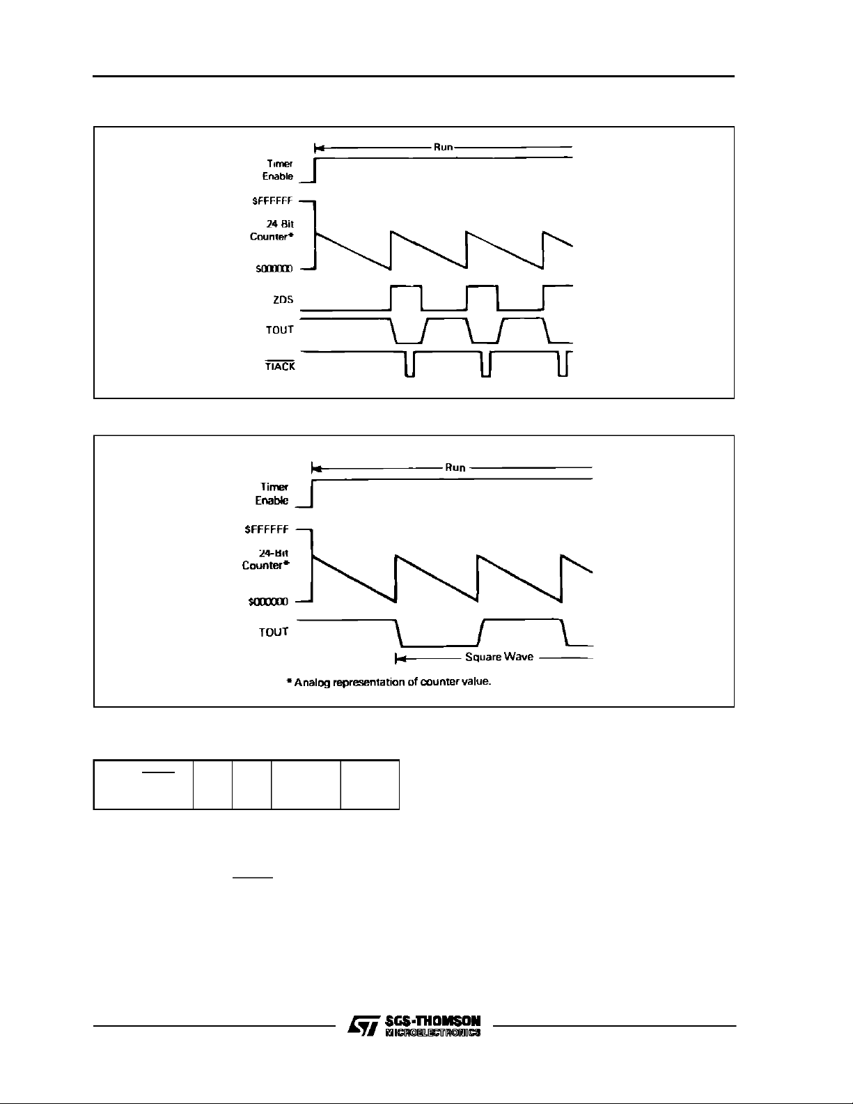
Figure 5.1 :Periodic Interrupt Generator Example.
*
Analog representation of counter value.
Figure 5.2 : Square WaveGenerator Example.
TS68230
5.2.3.INTERRUPTAFTER TIMEOUT.
765 4 32 1 0
TOUT/TIACK
Control
Z.D
Control
*
Clock
Control
Timer
Enable
0 1 x 0 0 00 or 1X Changed
Inthis configuration the timergeneratesan interrupt
after a programmed time period has expired. The
TOUT pin is connected to thesystem’s interrupt request circuitry and the TIACKpin may be an inter-
rupt acknowledge input to the timer. The TIN pin
may be used as a clockinput.
This configuration is similar to the periodic interrupt
generator exceptthatthezerodetect control bitisset.
Thisforcesthecounterto rolloverafterzerodetect is
reached, rather than reloading fromtheCPRs.When
theprocessor takes the interruptit canhaltthetimer,
read thecounter andcalculate thetimefromtheinterrupt request to entering the serviceroutine. Accurate
knowledge of the interrupt latency may be useful in
someapplications (see figure5.3).
45/61

TS68230
Figure 5.3 : Single Interrupt afterTimeout Example.
5.2.4. ELAPSED TIME MEASUREMENT EXAM-
PLES. Elapsed time measurement takes several
forms ; two forms are described in the following
paragraphs.
5.2.4.1. System Clock Example.
765 4 32 1 0
TOUT/TIACK
Control
Z.D
Control
*
Clock
Control
Timer
Enable
0 0 X 1 0 0 0 Changed
This configuration allows time interval measurement by software.The TIN pin may be used as an
external timer enable ifdesired.
Figure 5.4 : Elapsed Time Measurement Example.
The processor loads the counter preload registers
(generally with all ones), loads the timercontrol register,and thenenablesthe timer.Thecounter isallowed to decrement until the ending event takes
place.Whenitisdesired toreadthetimeinterval, the
processor must halt the timer and then read the
counter. If TIN is used as an enable, the start and
stop counterfunctions are controlled externally.
For applications in which the interval may exceed
theprogrammed time interval,zerodetectioncanbe
counted by polling the statusregister or through interrupts to simulate additional timer bits. Note that
the ZDS bit is latched and should be cleared after
eachdetection of zero. At the end, thetimer canbe
haltedand read (see figure5.4).
46/61

TS68230
5.2.4.2. External Clock.
765 4 32 1 0
TOUT/TIACK
Control
Z.D
Control
*
Clock
Control
Timer
Enable
0 0 X 1 0 1 X Changed
This configuration allows measurement (counting)
ofthenumber ofinputpulsesoccurring inaninterval
in which the counter is enabled. The TIN input pin
provides the inputpulses. Generally theTOUT and
TIACKpins are not used.
This configuration is similar to the elapsed time
measurement/system clock configuration except
thatthe TINpinis used toprovide theinput frequency.It canbeconnected toasimple oscillatorand the
same methods could be used. Alternately, it could
be gatedoff andon externally andthe number ofcyclesoccurring while inthe run statecanbecounted.
However, minimum pulse width highand lowspecificationsmust be met.
5.2.5.DEVICE WATCHDOG.
765 4 32 1 0
TOUT/TIACK
Control
Z.D
Control
*
Clock
Control
Timer
Enable
This configuration provides the watchdog function
needed in many systems. The TIN pin is the timer
input whose period at the high (one) level is to be
checked.Onceallowedbytheprocessor,theTINinput pin controls therun/halt mode. The TOUTpin is
connected to external circuitryrequiring notification
whenthe TINpinhas been assertedlongerthan the
programmed time. The TIACK pin (timer interrupt
acknowledge) is only needed if the TOUT pin is
connected to the interrupt circuitry.
The processor loads the counter preload register
and timer controlregister, and then enables the timer.When the TIN input isasserted(one, high)the
timer transfers the contents of the counter preload
register to the counter and begins counting. If the
TIN inputis negated before zero detect is reached,
the TOUToutput and the ZDS status bit remain negated.If zero detect is reached while the TIN input
is still asserted, the ZDS status bit is set and the
TOUT output is asserted. (The counter rolls over
and keeps counting). In either case, when the TIN
inputis negatedtheZDSstatusbitiszero,theTOUT
outputis negated, the counting stops, andtheprescaleris forcedto all ones (seefigure 5.5).
1 X 1 1 0 0 1 Changed
Figure 5.5 : Device Watchdog Example.
47/61

TS68230
SECTION 6
ELEC T RI CA L SPECIFICA T IONS
This sectioncontainselectrical specifications and associatedtiming information for theTS68230.
6.1 ABSOLUTE MAXIMUM RATINGS
Symbol Parameter Value Unit
V
V
T
T
This device contains circuitry to protect the inputs against damage due to high static voltages or electric fields ; however, it is
advised that normal precautions be taken to avoid application of any voltage higher than maximum-rated voltages to this high-
6.2 THERMAL DATA
Supply Voltage – 0.3 to + 7.0 V
CC
Input Voltage – 0.3 to + 7.0 V
IN
Operating Temperature Range
A
stg
TS68230C
TS68230V
Storage Temperature – 55 to + 150 °C
TLto T
0to+70
–40to+85
H
°C
θ
impedance circuit. Reliability of operation is enhanced if unused inputs are tied to an appropriate logic voltage level (e.g.,
either VSSor VCC).
Thermal Resistance Plastic 50 °C/W
JA
6.3. POWERCONSIDERATIONS
The average chip-junction temperature, TJ,in°C
can be obtained from :
TJ=TA+(PD• θ JA)
Where :
TA= Ambien t Temper ature, °C
θJA=Package Therma l Resistance, Junction-to-
Ambie nt,°C/W
PD=P
INT+PI/O
P
INT=ICCxVCC
, Watts - Chip Inte rnal Power
P
= PowerDissipation on Inputand Output Pins
I/O
-UserDetermined
Formostap plic ations P
I/O<PINT
andcan be neg lected.
An approximate rela tionship betwe en PDand TJ(if
P
is neglected) is :
I/O
PD=K (TJ+273°C)
Solvi ngequations 1 and2 for K gives :
K=PD•(TA+ 273°C) + θJA •P
2
D
Where K is a constant pertainin g to the particular
part.K can be determi ned from equation3 by measurin g PD(atequilibrium) fora knownTA. Usingthis
valueof Kthe valuesof PDandTJcanbe obtain ed
48/61

TS68230
6.4 DC ELECTRICAL CHARACTERISTICS (VCC= 5.0Vdc ± 5%, TA=TLto THunless otherwise noted)
Symbol Parameter Min. Max. Unit
V
V
I
I
V
V
P
C
6.5 AC ELECTRICAL SPECIFICATIONS – CLOCKTIMING (seefigure 6.1)
Input High Voltage All Inputs VSS+ 2.0 V
IH
Input Low Voltage All Inputs VSS– 0.3 VSS+ 0.8 V
IL
Input Leakage C urrent (VIN= 0 to 5.25V) H1, H3, R/W, RESET,
IN
CLK, RS1-RS5, CS
Hi-Z Input Current (VIN= 0.4 to 2.4) D0-D7 DTACK, PC0-PC7,
TSI
H2, H4, PA0-PA7, PB0-PB7 – 0.1
Output High Voltage
OH
OL
(I
Load
(I
Load
(I
Load
Output Low Voltage
(I
Load
(I
Load
(I
Load
= – 400µA, VCC=min)
= – 150µA, VCC=min)
= – 100µA, VCC=min)
= 8.8mA, VCC= min)
= 5.3mA, VCC= min)
= 2.4mA, VCC= min)
DTACK, D0-D7
H2, H4, PB0-PB7, PA0-PA7
PC0-PC7
PC3/TOUT, PC5/PIRQ
D0-D7, DTACK
PA0-PA7, PB0-PB7, H2, H4,
+ 2.4 V
V
SS
PC0-PC2, PC4, PC6, PC7
Internal Power Dissipation (measured at TA=0°C) 750 mW
INT
Input Capacitance (Vin=0,TA=25°C, f = 1MHz) 15 pF
IN
CC
10.0 µA
20
– 1.0
µA
mA
0.5 V
V
Symbol Parameter
8MHz 10MHz
Min. Max. Min. Max.
f Frequency of Operation 2.0 8.0 2.0 10.0 MHz
t
t
t
t
t
Cycle Time 125 500 100 500 ns
cyc
Clock Pulse Width 5555250
CL
CH
Rise and Fall Times 10
Cr
Cf
2504545
10
250
250
10
10
Figure 6.1 : Clock Input Timing Diagram.
Unit
ns
ns
49/61

TS68230
6.6. AC ELECTRICAL SPECIFICATIONS
(VCC= 5.0Vdc ± 5%, VSS= 0Vdc,TA=TLto THunless otherwise specified)
Read and Write Cycle Timings (figures 6.2 and6.3)
Number Par amet er
1 R/W, RS1-RS5 Valid to CS Low (setup time) 0 0 ns
(1)
2
3
4
CS Low to R/W and RS1-RS5 Invalid (hold time) 100 65 ns
(2)
CS Low to CLK Low (setup time) 30 20 ns
(3)
CS Low to Data Out Valid 75 60 ns
5 RS1-RS5 Valid to Data Out Valid 140 100 ns
6 CLK Low to DTACK Low (read/write cycle) 0 70 0 60 ns
(4)
7
DTACK Low to CS High (hold time) 0 0 ns
8 CS or PIACK or TIACK High to Data Out Invalid (hold time) 0 0 ns
9 CS or PIACK or TIACK High to D0-D7 High Impedance 50 45 ns
10 CS or PIACK or TIACK High to DTACK High 50 45 ns
11 CS or PIACK or TIACK High to DTACK High Impedance 100 55 ns
12 Data In Valid to CS Low (setup time) 0 0 ns
13 CS Low to Data in Invalid (hold time) 100 65 ns
23 CLK low on which DMAREQ is asserted to CLK low on
which DMAREQ is negated
28 Read Data Valid to DTACK Low (setup time) 0 0 ns
(5)
32
Synchronized CS to CLK low on which DMAREQ is asserted 3 3 3 3 CLK Per
35 CLK Low to DMAREQ Low (delay time) 0 120 0 100 ns
36 CLK Low to DMAREQ High (delay time) 0 120 0 100 ns
(5)
37
38
39 CLK Low to PIRQ Low or High Impedance 0 250 0 225 ns
40
Synchronized H1(H3) to CLK low on which PIRQ is asserted 3 3 3 3 CLK Per
(5)
Synchronized CS to CLK low on which PIRQ is high impedance 3 3 3 3 CLK Per
(6)
TIN Frequency (external clock) - Prescaler used. 0 1 0 1 f
41 TIN Frequency (external clock) - Prescaler not used. 0 1/8 0 1/8 f
42 TIN Pulse Width High or Low (external clock) 55 45 ns
43 TIN Pulse Width Low (run/halt control) 1 1 CLK Per
44 CLK Low to TOUT High, Low, or High Impedance 0 250 0 225 ns
45 CS, PIACK, or TIACK High to CS, PIACK, or TIACK Low 50 30 ns
by solving equations (1) and (2) iterativelyfor any valueof TA.
8MHz 10MHz
Min. Max. Min. Max.
2.5 3 2.5 3 CLK Per
Unit
(Hz)
(Hz)
clk
clk
(7 )
(7 )
Notes : 1. See 1.4. Bus Interface Operation for exception.
2. This specification only applies if the PI/T had completed all operations initiated by the previous bus cycle when CS
was asserted. Following a normal read or write bus cycle, all operations are complete within three clocks after the
falling edge of the CLK pin on which DTACK was asserted. If CS is asserted prior to completion of these operations, the new bus cycle, and hence, DTACK is postponed.
If all operations of the previous bus cycle were complete when CS was asserted, this specification is made only to
insure that DTACK is asserted with respect to the falling edge of the CLK pin as shown in the timing diagram, not
to guarantee operation of the part. If the CS setup time is violated, DTACK may be asserted as shown, or may be
asserted one clock cycle later.
3. Assuming the RS1-RS5 to data valid time has also expired.
4. This specification imposes a lower bound on CS low time, guaranteeing that CS will be low for at least 1 CLK period.
5. Synchronized means that the input signal has seen seen by the PI/T on the appropriate edge of the clock (rising
edge for H1(H3) and falling edge for CS). (Refer to the 1.4. Bus Interface Operation for the exception concerning
CS).
6. This limit applies to the frequency of the signal at TIN compared to the frequency of the CLK signal during each
clock cycle. If any period of the waveform at TIN is smaller than the period of the CLK signal at that instant, then
it is likely that the timer circuit will completely ignore one cycle of the TIN signal.
If these two signals are derived from different sources they will have different instantaneous frequency variations. In
this case the frequency applied to the TIN pin must be distinctly less than the frequency at the CLK pin to avoid lost
cycles of the TIN signal. With signals derived from different crystal oscillators applied to the TIN and CLK pins with
50/61

Figure 6.2 : Read CycleTiming Diagram.
Figure 6.3 : Write Cycle Timing Diagram.
TS68230
51/61

TS68230
6.6. AC ELECTRICALSPECIFICATIONS
(VCC= 5.0Vdc ± 5%, VSS= 0Vdc, TA=TLto THunless otherwise noted)
Peripheral Input Timings (figures 6.4)
Number Para me ter
8MHz 10MHz
Min. Max. Mi n. M a x.
14 Port Input Data Valid to H1(H3) Asserted (setup time) 100 60 ns
15 H1(H3) Asserted to Port Input Data Invalid (hold time) 20 20 ns
16 Handshake Input H1(H4) Pulse Width Asserted 40 40 ns
17 Handshake Input H1(H4) Pulse Width Negated 40 40 ns
18 H1(H3) Asserted to H2(H4) Negated (delay time) 150 120 ns
19 CLK Low to H2(H4) Asserted (delay time) 100 100 ns
(1 )
20
21
22
23 CLK low on which DMAREQ is asserted to CLK low on which
H2(H4) Asserted to H1(H3) Asserted 0 0 ns
(2 )
CLK Low to H2(H4) Pulse Negated (delay time) 125 125 ns
(3.4)
Synchronized H1(H3) to CLK low on which DMAREQ is asserted 2.5 3.5 2.5 3.5 CLK Per
2.5 3 2.5 3 CLK Per
DMAREQ is negated
(5 )
30
33
H1(H3) Asserted to CLK High (setup time) 50 40 ns
(3.4)
Synchronized H1(H3) to CLK low on which H2(H4) is asserted 3.5 4.5 3.5 4.5 CLK Per
35 CLK Low to DMAREQ Low (delay time) 0 120 0 100 ns
36 CLK Low to DMAREQ High (delay time) 0 120 0 100 ns
If these two signals are derived from different sources they will have different instantaneous frequency variations. In
this case the frequency applied to the TIN pin must be distinctly less than the frequency at the CLK pin to avoid lost
cycles of the TIN signal. With signals derived from different crystal oscillators applied to the TIN and CLK pins with
fast rise and fall times, the TIN frequency can approach 80 to 90% of the frequency of the CLK signal without a loss
of a cycle of the TIN signal.
If these signals are derived from the same frequency source then the frequency of the signal applied to TIN can be
100% of the frequency at the CLK pin. They may be generated by different buffers from the same signal or one
may be an inverted version of the other. The TIN signal may be generated by an ’AND’ function of the clock and a
control signal.
Unit
52/61

Figure 6.4 : Peripheral Input Timing Diagram.
TS68230
Note :Timingmeasurements are referenced toand from a low voltage of 0.8voltand a high voltageof 2.0volts, unless otherwise noted.
7. CLK refers to the actual frequency of the CLK pin, not the maximum allowable CLK frequency.
Notes : 1. This specification assures recognition of the asserted edge of H1(H3).
53/61

TS68230
6.6. AC ELECTRICAL SPECIFICATIONS
(VCC= 5.0Vdc ± 5%, VSS= 0Vdc, TA=TLto THunless otherwise noted)
Peripheral Output Timings (figures 6.5)
Number Parameter
8MHz 10M Hz
Min. Max . Min. Max.
16 Handshake Input H1(H4) Pulse Width Asserted 40 40 ns
17 Handshake Input H1(H4) Pulse Width Negated 40 40 ns
18 H1(H3) Asserted to H2(H4) Negated (delay time) 150 120 ns
19 CLK Low to H2(H4) Asserted (delay time) 100 100 ns
(1 )
20
21
22
23 CLK low on which DMAREQ is asserted to CLK low on which
H2(H4) Asserted to H1(H3) Asserted 0 0 ns
(2 )
CLK Low to H2(H4) Pulse Negated (delay time) 125 125 ns
(3.4)
Synchronized H1(H3) to CLK low on which DMAREQ is asserted 2.5 3.5 2.5 3.5 CLK Per
2.5 3 2.5 3 CLK Per
DMAREQ is negated
24 CLK Low to Port Output Data Valid (delay time) (modes 0 and 1) 150 120 ns
(3.4)
25
Synchronized H1(H3) to Port Output Data Invalid (modes 0 and 1) 1.5 2.5 1.5 2.5 CLK Per
26 H1 Negated to Port Output Data Valid (modes 2 and 3) 70 50 ns
27 H1 Asserted to Port Output Data High Impedance (modes 2 and 3) 0 70 0 70 ns
(5 )
30
H1(H3) Asserted to CLK High (setup time) 50 40 ns
35 CLK Low to DMAREQ Low (delay time) 0 120 0 100 ns
36 CLK Low to DMAREQ High (delay time) 0 120 0 100 ns
2. This specification applies only when a pulsed handshake option is chosen and the pulse is not shortened due to an
early asserted edge of H1(H3).
3. The maximum value is caused by a peripheral access (H1(H3) asserted) and bus access ( CS asserted) occurring
at the same time.
4. Syncrhonized means that the input signal has been seen by the PI/T on the appropriate edge of the clock (rising
edge for H1(H3) and falling edge for CS). (Refer to the 1.4 Bus Interface Operation for the exception concerning
CS).
5. If the setup time on the rising edge of the clock is not met, H1(H3) may not be recognized until the next rising of
the clock.
Unit
54/61

Figure 6.5 : Peripheral OuputTiming Diagram.
TS68230
Notes : 1. Timing diagram shows H1, H2, H3, and H4 asserted low.
2. Timing measurements are referenced to and from a low voltage of 0.8volt and a high voltage of 2.0volts, unless
otherwise noted.
55/61

TS68230
6.6. AC ELECTRICAL SPECIFICATIONS
(VCC= 5.0Vdc ± 5%, VSS= 0Vdc,TA=TLto THunless otherwise noted)
Iack Timings (figure 6.6)
Number Par amet er
8 CS or PIACK or TIACK High to Data Out Invalid (hold time) 0 0 ns
9 CS or PIACK or TIACK High to D0-D7 High Impedance 50 45 ns
10 CS or PIACK or TIACK High to DTACK High 50 45 ns
11 CS or PIACK or TIACK High to DTACK High Impedance 100 55 ns
29 CLK Low to Data Output Valid, Interrupt Acknowledge Cycle 120 100 ns
31 PIACK or TIACK Low to CLK Low (setup time) 50 40 ns
34 CLK Low to DTACK Low Interrupt Acknowledge Cycle (delay time) 100 100 ns
8MHz 10MHz
Min. Max. Min. Max.
Figure 6.6 : IACK TimingDiagram.
Unit
Notes : 1. This specification assures recognition of the asserted edge of H1(H3).
56/61

2. This specification applies only when a pulsed handshake option is chosen and the pulse is not shortened due to an
early asserted edge of H1(H3).
3. The maximum value is caused by a peripheral access (H1(H3) asserted) and bus access ( CS asserted) occurring
at the same time.
4. Synchronized means that the input signal has been seen by the PI/T on the appropriate edge of the clock (rising
edge for H1(H3) and falling edge for CS). (Refer to the 1.4. Bus Interface Operation for the exception concerning
CS).
7.1. PIN ASSIGNMENTS
48-Pin Dual-in-Line 52-Pin QuadPack (PLCC)
TS68230
57/61

TS68230
7.2. PACKAGE MECHANICAL DATA
mm
mm
58/61

Table 1.3 : Register Model (sheet 2 of 2).
Register
Register
Select Bits
5432176543210
1 0 0 0 0 TOUT/TIACK
Control
10001 Bit7Bit
6
10010 ✶✶✶✶✶✶✶✶ 0 0 (null)
Bit
ZD
Ctrl
Bit
5
4
✶ Clock
Control
Bit
3
Bit
2
Bit
Timer
Enable
Bit
1
0
Value
after
RESET
(hex
value)
0 0 Timer Control
Register
0 F Timer Interrupt
Vector Register
TS68230
10011 Bit23Bit
22
10100 Bit15Bit
14
10101 Bit7Bit
6
10110 ✶✶✶✶✶✶✶✶ 0 0 (null)
10111 Bit23Bit
22
11000 Bit15Bit
14
11001 Bit7Bit
6
11010 ✶✶✶✶✶✶✶ZDS 0 0 Timer Status
11011 ✶✶✶✶✶✶✶✶ 0 0 (null)
11100 ✶✶✶✶✶✶✶✶ 0 0 (null)
11101 ✶✶✶✶✶✶✶✶ 0 0 (null)
11110 ✶✶✶✶✶✶✶✶ 0 0 (null)
Bit
21
Bit
13
Bit
Bit
21
Bit
13
Bit
Bit
20
Bit
12
Bit
5
5
4
Bit
20
Bit
12
Bit
4
Bit
19
Bit
11
Bit
Bit
19
Bit
11
Bit
Bit
18
Bit
10
Bit
3
3
2
Bit
18
Bit
10
Bit
2
Bit
17
Bit
Bit
Bit
17
Bit
Bit
Bit
16
Bit
9
1
9
1
8
Bit
0
Bit
16
Bit
8
Bit
0
✶✶ Counter Preload
Register (high)
✶✶ Counter Preload
Register (mid)
✶✶ Counter Preload
Register (low)
✶✶ Count Register
(high)
✶✶ Count Register
(mid)
✶✶ Count Register
(low)
Register
11111 ✶✶✶✶✶✶✶✶ 0 0 (null)
Unused, read as zero.
*
59/61

TS68230
Table 1.3 : Register Model (sheet 1 of 2).
Register
Register
Select Bits
5432176543210
0 0 0 0 0 Port Mode
Control
00001 ✶ SVCRQ
00010 Bit7Bit
00011 Bit7Bit
00100 Bit7Bit
0 0 1 0 1 Interrupt Vector
0 0 1 1 0 Port A
Submode
0 0 1 1 1 Port B
Submode
01000 Bit7Bit
01001 Bit7Bit
01010 Bit7Bit
01011 Bit7Bit
01100 Bit7Bit
01101 H4
LevelH3LevelH2LevelH1Level
01110 ✶✶✶✶✶✶✶✶ 0 0 (null)
Select
6
6
6
6
6
6
6
6
H34
Enable
Bit
Bit
Bit
Bit
Bit
Bit
Bit
Bit
H12
EnableH4SenseH3SenseH2SenseH1Sense
IPF
Select
Bit
5
5
5
5
5
5
5
5
4
Bit
4
Bit
4
Number
H2 Control H2
H4 Control H4
Bit
4
Bit
4
Bit
4
Bit
4
Bit
4
Port Interrupt
Priority Control
Bit
3
Bit
3
Bit
3
Bit
3
Bit
3
Bit
3
Bit
3
Bit
3
H4S H3S H2S H1S ✶✶ ✶✶ Port Status
Bit
2
Bit
2
Bit
2
Int
Enable
Int
Enable
Bit
2
Bit
2
Bit
2
Bit
2
Bit
2
Bit
1
Bit
1
Bit
1
✶✶ 0 F Port Interrupt
H1
SVCRQ
Enable
H3
SVCRQ
Enable
Bit
1
Bit
1
Bit
1
Bit
1
Bit
1
Bit
0
Bit
0
Bit
0
H1
Stat
Ctrl
H3
Stat
Ctrl
Bit
0
Bit
0
Bit
0
Bit
0
Bit
0
Value
after
RESET
(hex
value)
0 0 Port General
Control Register
0 0 Port Service
Request Register
0 0 Port A Data
Direction Register
0 0 Port B Data
Direction Register
0 0 Port C Data
Direction Register
Vector Register
0 0 Port A Control
Register
0 0 Port B Control
Register
✶✶ Port A Data
Register
✶✶ Port B Data
Register
✶✶✶ Port A Alternate
Register
✶✶✶ Port B Alternate
Register
✶✶✶✶ Port C Data
Register
Register
01111 ✶✶✶✶✶✶✶✶ 0 0 (null)
Unused, read as zero.
*
Value before RESET.
**
Current value on pins.
***
60/61

SECT IO N 8
ORDER CODES
8.1. STANDARD VERSIONS
Par t N u mber Frequenc y (MHz) Temperature Range Package T ype
TS68230CP8
TS68230CP10
TS68230CFN8
TS68230CFN10
8.0
10.0
8.0
10.0
0°Cto+70°C
0°Cto+70°C
0°Cto+70°C
0°Cto+70°C
TS68230
Plastic DIL
P Suffix
PLCC
FN Suffix
Information furnished is believed to be accurate and reliable. However, SGS-THOMSON Microelectronics assumes no
responsability for the consequences of use of such information nor for any infringement of patents or other rights of
third parties which may result from its use. No license is granted by implication or otherwiseunder any patent or patent
rights of SGS-THOMSON Microelectronics. Specifications mentioned in this publication are subject to change without
notice. This publication supersedes and replaces all information previously supplied.
SGS-THOMSON Microelectronics products are not authorized for use as critical components in life support devices or
systems without the express written approval of SGS-THOMSON Microelectronics.
1994 SGS-THOMSON Microelectronics - All rights reserved.
Purchase of I2C Components by SGS-THOMSON Microelectronics conveys a license under the Philips I2C Patent.
Rights to use these components in an I2C system is granted provided that the system conforms to the I2C Standard
SGS-THOMSON Microelectronics Group of Companies
Australia - Brazil - France - Germany - Hong Kong - Italy - Japan - Korea - Malaysia - Malta - Morocco
The Netherlands Singapore- Spain - Sweden - Switzerland - Taiwan - Thailand - United Kingdom - U.S.A.
Specification as defined by Philips.
61/61
 Loading...