

1/9
■ LOW NOISE : 4.7nV/√Hz
■ LOW DISTORTION
■ HIGH SLEW RATE : 90V/µs
■ WIDE BANDWIDTH : 52MHz @ -3dB &
18dB gain
■ GAIN PROGRAMM A BLE from -9dB to +30dB
with 3dB STEPS
■ POWER DOWN FUNCTION
DESCRIPTION
This TS636 is particularly intended for applications such as preamplification in telecommunication systems using m ultiple carriers. It has been
minly designed to fit with ADSL chip-sets such as
ASCOT ADSL chip-set for CPE.
The TS636 is a differential digitally con troled variable gain amplifier featuring a high slew rate of
90V/µs, a large bandwidth, a very low distortion
and a very low current and voltage noise.
The gain can be set from -9dB to +30dB through a
4bit digital word, with 3dB steps.
The gain monotonicity is guaranteed by design.
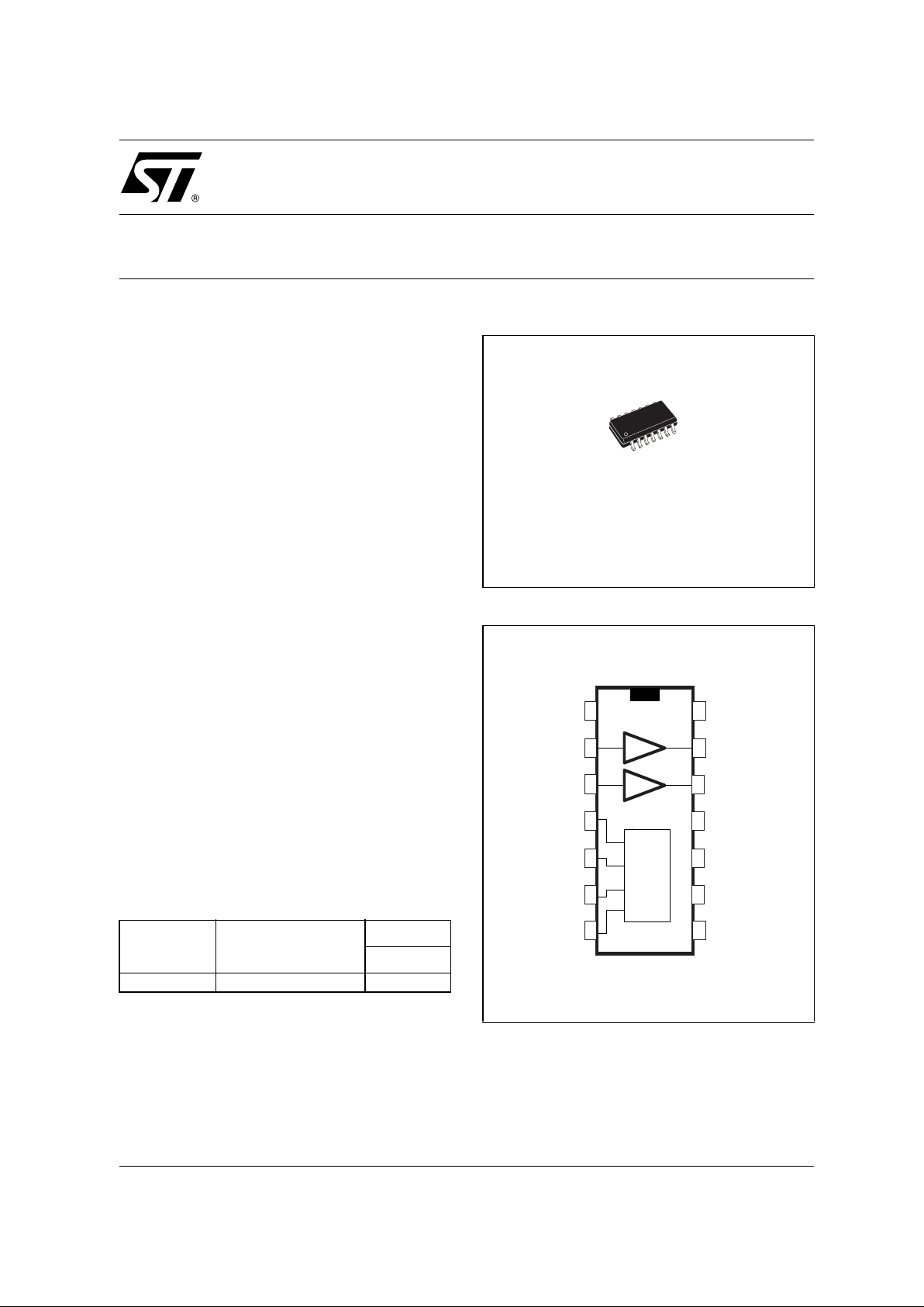
The TS636 comes in SO-14 plastic packages.
APPLICATION
■ Preamplifier with automatic gain control for
Asymmetric Digital Subscriber Line (ADSL).
ORDER CODE
D = Small Outline Package (SO) - also available in Tape & Reel (DT)
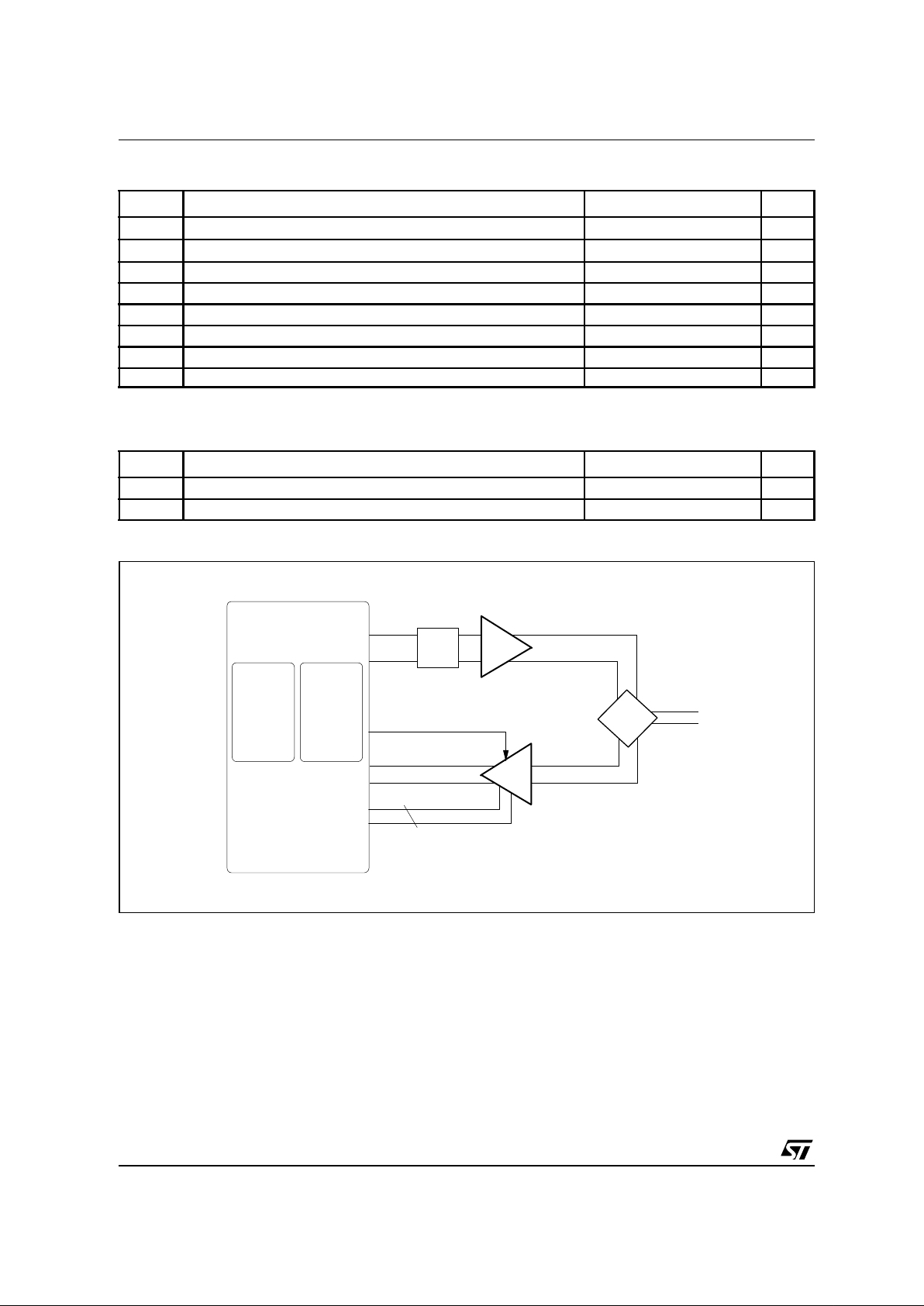
PIN CONNECTIONS (top view)
Part Number Temperature Range
Package
D
TS636I -40, +85°C
•
D
SO14
(Plastic Micropackage)
+Vcc2
Inpu t 1
Input 2
-Vcc
DGND
LSB
GC1
GC2
GC3
MSB GC4
Output 1
1
2
3
4
5
6
7
14
13
12
11
10
9
8
Output 2
AGND
Power Down
+Vcc1
Gain Control
Logic Dec oder
TS636
DIFFERENTIAL VARIABLE GAIN AMPLIFIER
FOR ADSL LINE INTERFACE
January 2001
TS636
2/9
ABSOLUTE MAXIMUM RATINGS
OPERATING CONDITIONS
APPLICATION: ADSL LINE INTERFACE
Symbol Parameter Value Unit
V
CC
Supply voltage
1)
14 V
V
i
Input Voltage
2)
0 to 14 V
T
oper
Operating Free Air Temperature Range TS636ID -40 to + 85 °C
T
std
Storage Temperature -65 to +150 °C
T
j
Maximum Junction Temperature 150 °C
R
thjc
Thermal Resistance Junction to Case 22 °C/W
R
thja
Thermal Resistance Junction to Ambiante Area 125 °C/W
Output Short Circuit Duration Infinite
1. All voltages values are with respect to network terminal.
2. The magnitude of input and output voltages must never exceed V
CC
+0.3V.
Symbol Parameter Value Unit
V
CC
Supply Voltage 5 to 12 V
V
icm
Common Mode Input Voltage
V
CC
/2
V
twisted-pair
telephone
line
HYBRID
CIRCUIT
LP filter
TS634 or TS635
Line Driver
reception
(analog signal)
emission
(analog
signal)
upstream
downstream
ST70135 ST70134
TS636
Receiver
VGA
ASCOT ADSL
CHIP-SET
Power Down
4-bit Gain Cont rol
TX
RX
TS636
3/9
ELECTRICAL CHARACTERISTICS. VCC = ±6Volts, T
amb
= 25°C (unless otherwise specified).
Symbol Parameter Test Condition Min. Typ. Max Unit
DC PERFORMANCE
I
ib
Input Bias Current (AGND pin) 8
µ
A
I
CC
Total Supply Current
No load, V
out
= 0
28 mA
∆
V
OFFSET
Differential Input Offset Voltage
V
in
= 0, AV = 30dB
6mV
SVR Supply Voltage Rejection Ratio
A
V
= 0dB
50 80 dB
POWER DOWN MODE
I
ccpdw
Power Down Total Consumption Power Down Mode 150
µ
A
Z
out
Power Down Output Impedance Power Down Mode 100kΩ150kΩ//5pF
AC PERFORMANCE
Z
in
Input Impedance 100kΩ//5pF
V
OH
High Level Output Voltage
R
L
connected to GND
R
L
= 500
Ω
4 4.5 V
V
OL
Low Level Output Voltage
R
L
connected to GND
R
L
= 500
Ω
-4.5 -4 V
A
V
Voltage Gain F= 1MHz
-9 30 dB
Gain monotonicity guaranteed by design
P
AV
Precision of the Voltage Gain F= 1MHz -1.4 1.4 dB
A
vstep
Step Value F= 1MHz 2.4 3 3.6 dB
A
vmis
Gain Mismatch between Both
Channels
F= 1MHz 1 dB
B
w
Bandwidth @ -3dB
R
L
= 500Ω, CL = 15pF
A
V
= -9dB
45 100 MHz
A
V
= +30dB
917 MHz
R
bw
Bandwidth Roll-off
A
V
= +30dB, F = 1MHz
0.08 dB
I
o
Bandwidth @ -3dB
R
L
= 500Ω, CL = 15pF
|Source| 17 28
mA
Sink 17 22
SR Slew Rate (gain independent)
V
o
= 2Vpeak
40 90 V/µs
NOISE AND DISTORTION
in Equivalent Input Noise Current F = 100kHz 1.6 pA/√Hz
en Equivalent Input Noise Voltage
F = 100kHz
A
V
= 30dB
4.7 nV/√Hz
THD30 Harmonic Distorsion
1Vpeak, F = 150kHz,
A
V
= +30dB, RL = 500Ω//15pF
dBc
H2 -70
H3 -93
H4 -98
H5 -99
IM3_1
Third Order Intermodulation
Product
F1 = 180kHz, F2 = 280kHz
V
out
= 1Vpeak, AV = +30dB
R
L
= 500Ω//15pF
dBc
@ 80kHz -77
@ 380kHz -85
@640kHz -86
@740kHz -87
IM3_2
Third Order Intermodulation
Product
F1 = 70kHz, F2 = 80kHz
V
out
= 1Vpeak, AV = +30dB
R
L
= 500Ω//15pF
dBc
@ 60kHz -77
@ 90kHz -79
@220kHz -83
@230kHz -84

TS636
4/9
DIGI T AL INPUTS
SIMPLIFIED SCHEMATIC
The TS636 consists of two independent channels.
Each channel has two stages. The first is a very low noise digitally controlled variable gain amplifier (range
0 to 18dB).
The TS636 features a high input impedance and a low noise current. To minimize the overall noise figure,
the source impedance must be less than 3kΩ.
This value gives an equal contribution of voltage and current noises.
The second stage is a gain/attenuation stage (+12dB to -9dB) featuring a low output impedance.
This output stage can drive loads as low as 500Ω.
POWER DOWN MODE POSITION
Pin Parameter Min. Typ. Max. Unit
GC1, GC2, GC3
and GC4
Low Level 0 0.8
V
High Level 2 3.3
Power Down
Thershold Voltage for Power
Down Mode (high level active)
0 0.8
V
23.3
+
_
_
+
+
_
_
+
v
v
GAIN CON TROL
LOGIC DECODER
Input1
+
_
_
+
v
Input2
+Vcc2
Digital GND
(DGND)
Ouput2
Ouput1
+Vcc1
-Vcc
Analog GND
(AGND)
GC2
GC1
GC3
GC4
v
v
v
Power
Down
+Vcc
-Vcc
+Vcc
-Vcc
Power Down
Input Output

TS636
5/9
BANDWIDTH
The small signal bandwidth is almost constant for gains between +18dB to 0dB and is in the order of
52MHz to 70MHz respectively. For 30dB gain the bandwidth is around 18MHz.
The power bandwidth is typically equal to 30MHz for 2V peak to peak signals.
MAXIMUM INPUT LEVEL
The input level must not exceed the following values :
negative peak value: must be greater than -V
CC
+ 1.5V
positive peak value: must be less than +V
CC
- 1.5V
For example, if a
±6V power supply is used, the input signal can swing between -4.5V and +4.5V.
These values are due to common mode input range limitations of the input stage of the first amplifier.
Some other limitations may occur, due to the slew rate of the first operational amplifier (typically in the or-
der of 300V/µs). This means that the maximum input signal decreases at high frequency.
SINGLE SUPPLY OPERATI ON
The incoming signal is AC coupled to the inputs.
The TS636 can be used either with a dual or a single supply. If a single supply is used, the inputs are bi-
ased to the mid supply voltage (+V
CC/2
). This bias network m ust be carefully designed, in ord er to reject
any noise present on the supply rail.
The AGND pin (9) must be connected to +V
CC/2
. The bias current of the second stage (inverting structure)
is 8µA for both amplifiers. A resistor divider structure can be used. Two resistances should be chosen by
considering 8µA as the 1% of the total current through these resistances. For a single +12V supply voltage, two resistances of 7.5kΩ can be used. The differential input consists of a high pass circuit, formed by
the 1µF capacitor and a 1kΩ resistance and gives a break frequency of 160Hz.
SINGLE +12V SUP PLY OF THE TS 636
+Vcc2
Input 1
Input 2
-Vcc
DGND
GC1
GC2
GC3
GC4
Output 1
1
2
3
4
5
6
7
14
13
12
11
10
9
8
Output 2
AGND
Power Down
+Vcc1
Gain Control
Logic Decoder
10nF 1µF
7.5k
7.5k
12V
10nF 1µF
47k
47k
12V
1k
1k
IN+
IN-
10nF
100nF 10µF
12V
10nF
100nF
1µF
1µF
TS636

TS636
6/9
GAIN CONTROL
The gain and the power down mode is programmed with a 4 bit digital word :
The gain is the same for both channels.
The digital inputs are CMOS compatible. The supply voltage of the logic decoder used to transcode the digital word can be either 3.3V or 5V or VCC.
Digital
Control
GC4....GC1
MSB LSB
Total Gain
(dB)
First Stage
Gain
(dB)
Second Stage
Gain
(dB)
Maximum
Input Level
Bandwidth
Small Signal
Eq. Input
Noise
(nV/√Hz)
$0000 -9 0 -9 2.8Vrms 110MHZ 29
$0001 -6 0 -6 2.8Vrms 100MHz 26
$0010 -3 0 -3 2.8Vrms 85MHz 23
$0011 0 0 0 2.8Vrms 69MHz 22
$0100 3 3 0 2Vrms 63MHz 16
$0101 6 6 0 1.4Vrms 58MHz 12
$0110 9 9 0 1Vrms 56MHz 9
$0111 12 12 0 0.7Vrms 55MHz 7
$1000 15 15 0 0.5Vrms 54MHz 6
$1001 18 18 0 0.35Vrms 52MHz 4.8
$1010 21 21 3 0.25Vrms 42MHz 4.7
$1011 24 24 6 175mVrms 30MHz 4.7
$1100 27 27 9 125mVrms 24MHz 4.6
$1101 30 30 12 88mVrms 18MHz 4.6
$1110 30 30 12 88mVrms 18MHz 4.6
$1111 30 30 12 88mVrms 18MHz 4.6

TS636
7/9
Closed Loop Gain vs. Frequency
Negative & Positive Slew Rate vs. Gain
Gain Switching (+15dB to -9dB)
Bandwidth vs. Gain
Equivalent Input Voltage Noise vs. Gain
Gain Switching (+30dB to +9dB)
-40
-30
-20
-10
0
10
20
30
40
Gain (dB)
10kHz 100kHz 1MHz 10MHz
100MHz
Frequency
-9 -6 -3 0 3 6 9 12 15 18 21 24 27 30
GAIN (dB)
70
75
80
85
90
95
100
105
110
SLEW RATE (V/µs)
SR+
SR-
Time
-4
-3
-2
-1
0
1
2
3
4
5
6
Ouput Sign al (V)
0
5µs
10µs 15µs
20µs
GC4 command
Ouput Signal
-9 -6 -3 0 3 6 9 12 15 18 21 24 27 30
GAIN (dB)
10
20
30
40
50
60
70
80
90
100
BANDWIDTH (MHz)
-9 -6 -3 0 3 6 9 12 15 18 21 24 27 30
GAIN (dB)
0
2
4
6
8
10
12
14
16
18
20
22
24
26
28
30
VOLTAGE NOISE (nV/VHz)
-4
-3
-2
-1
0
1
2
3
4
5
6
Ouput Signal (V)
0
5µs
10µs
15µs
20µs
Time
GC1 command
Ouput Signal
measurement conditions: Vcc=±6V, Rload=500
Ω,
Tamb=25°C

TS636
8/9
Output/Input Isolation in Power Down Mode vs.
Freque ncy
3rd Order In term odulation
(2 tones : 180kHz and 280kHz)
3rd Order In term odulation
(2 tones : 180kHz and 280kHz)
10kHz
100kHz 1MHz
10MHz
-110
-100
-90
-80
-70
-60
-50
Isolation (dB)
Frequency
012345
Vout peak (V)
-90
-85
-80
-75
-70
IM3 (dBc)
80kHZ
380kHZ
640kHZ
740kHZ
012345
Vout peak (V)
-90
-85
-80
-75
-70
IM3 (dBc)
60kHZ
90kHZ
220kHZ
230kHZ
measurement conditions: Vcc=±6V, Rload=500
Ω,
Tamb=25°C

TS636
9/9
Information furnished is beli eved to be accurate and reliable. However, STMicroe lectronics assumes no responsibility for the
consequences of use of such information nor for any infringement of patents or other rights of third parties which may result from
its use. No licens e is granted by implication or otherwise unde r any patent or patent rights of STMicroelectronics. Specifications
mentioned in this publication ar e subject to change without notice. This publication supersedes and replaces all information
previously supplied. S TMicroelectronics products are not authorized for use as critica l components in life suppo rt devices or
systems without express written approval of STMicroelectronics.
© The ST logo is a registered trademark of STMicroelectronics
© 2001 STM i cr o electro n ics - Printed in Italy - All Rights Res erved
STMicr oelectronics GROUP OF COMP ANIES
Australi a - Brazil - Chi na - Finlan d - F rance - Germany - Hong Kong - India - It al y - Japan - Mal aysia - Malta - Morocco
Singapo re - Spain - Sweden - Swit zerland - Un i ted Kingdom
© http://www.st.com
PACKAGE MECHANICAL DATA
14 PINS - PLASTIC MICROPACKAGE (SO)
Dim.
Millimeters Inches
Min. Typ. Max. Min. Typ. Max.
A 1.75 0.069
a1 0.1 0.2 0.004 0.008
a2 1.6 0.063
b 0.35 0.46 0.014 0.018
b1 0.19 0.25 0.007 0.010
C 0.5 0.020
c1 45° (typ.)
D (1) 8.55 8.75 0.336 0.344
E 5.8 6.2 0.228 0.244
e 1.27 0.050
e3 7.62 0.300
F (1) 3.8 4.0 0.150 0.157
G 4.6 5.3 0.181 0.208
L 0.5 1.27 0.020 0.050
M 0.68 0.027
S 8° (max.)
Note : (1) D and F do not include mold flash or protrusions - Mold flash or protrusions shall not exceed 0.15mm (.066 inc) ONLY FOR DATA B OOK.
 Loading...