

Datasheet TS634IPT, TS634IP, TS634IDT, TS634ID, TS634 Datasheet (SGS Thomson Microelectronics)
1/9
■ LOW NOISE : 3.2nV/√Hz, 1.5pA/√Hz
■ HIGH OUTPUT CURRENT : 160mA min.
■ VERY LOW HARMONIC AND INTERMODU-
LATION DISTO RTION
■ HIGH SLEW RATE : 40V/µs
■ SPECIFIED FOR 25Ω LOAD
DESCRIPTION
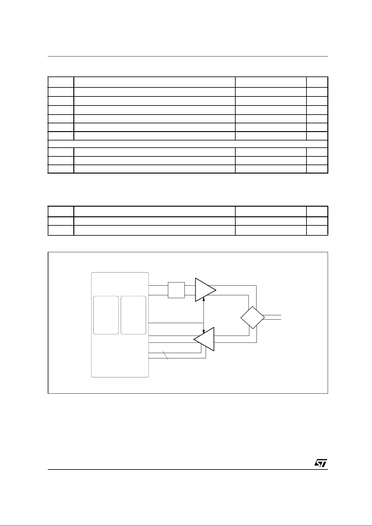
This device is particularly intended for applications
where multiple carriers must be amplified simultaneously with very low intermodulation products. It
has been mainly designed to fit with ADSL
chip-set such as ST70134 or ST70135.
The TS634 is a high output current dual operational amplifier, with a large gain-band width product
(130MHz) and capable of driving a 25Ω load at
12V power supply. The TS634 is fitted out with
Power Down function in order to decrease the
consumption.
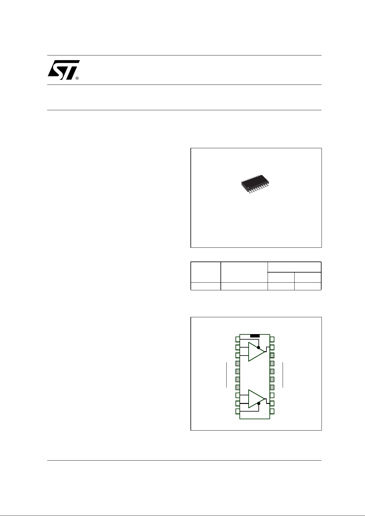
The TS634 is housed in SO20 batwing plastic
package for a very low thermal resistance.
APPLICATION
■ UPSTREAM line driver for Asymmetric Digital
Subs criber Line (ADSL) (NT).
ORDER CODE
D=Small Outline Package (SO) - also available in Tape & Reel (DT)
PIN CONNECTIONS (top view)
Part
Number
Temperature
Range
Package
DP
TS634ID -40, +85°C
•
D
SO20 Batwing
(Plastic Micropackage)
Vcc+ 1
Inverting input 1
Non-inver ting i nput 1
Vcc+ 2
Vcc -
Vcc -
Power Down 2
Non-Inverting i nput 2
Inverting input 2
GND
Vcc -
Vcc -
Vcc -
Vcc -
Vcc -
Vcc -
Power Down 1
Vcc-
Output 1
Output 2
1
2
3
4
5
6
7
8
9
10
20
19
18
17
16
15
14
13
12
11
_
+
_
+
SO20 batwing - To p V iew
Thermal Heat Tabs
connected to -Vcc
Thermal Heat Tabs
connected to -Vcc
TS634
DUAL WIDE BAND OPERATIONAL AMPLIFIER
FOR ADSL LINE INTERFACE
March 2003
TS634
2/9
ABSOLUTE MAXIMUM RATINGS
OPERATING CONDITIONS
APPLICATION: ADSL LINE INTERFACE
Symbol Parameter Value Unit
V
CC
Supply voltage
1)
±7 V
V
id
Differential Input Voltage
2)
±2 V
V
in
Input Voltage Range
3)
±6 V
T
oper
Operating Free Air Temperature Range TS634TS634ID -40 to +85 °C
T
std
Storage Temperature -65 to +150 °C
T
j
Maximum Junction Temperature 150 °C
SO20-Batwing
R
thjc
Thermal Resistance Junction to Case 25 °C/W
R
thja
Thermal Resistance Junction to Ambient Area 45 °C/W
P
max.
Maximum Power Dissipation (@25°C) 2.7 W
1. All voltages values, except differential voltage are with respect to network terminal.
2. Differential voltages are non-inverting input terminal with respect to the inverting input terminal.
3. The magnitude of input and output voltages must never exceed V
CC
+0.3V.
Symbol Parameter Value Unit
V
CC
Supply Voltage ±2.5 to ±6 V
V
icm
Common Mode Input Voltage
(V
CC
) +2 to (V
CC
+
) -1
V
twiste d-pair
telephone
line
HYBRID
CIRCUIT
LP filter
TS634
Line Driver
reception
(analog signal)
emission
(analog
signal)
upstream
downstream
ST70135 ST70134
TS636
Receiver
VGA
ASCOT ADSL
CHIP-SET
Power Down
4-bit Gain C ontrol
TX
RX
TS634
3/9
ELECTRICAL CHARACTERISTICS VCC = ±6Volts, T
amb
= 25°C (unless otherwise specified)
Symbol Parameter Test Condition Min. Typ. Max. Unit
DC PERFORMANCE
∆
V
io
Differential Input Offset Voltage
T
amb
= 25°C
6mV
I
io
Input Offset Current
T
amb
0.2 3
µ
A
T
min.
< T
amb
< T
max.
5
I
ib
Input Bias Current
T
amb
515
µ
A
T
min.
< T
amb
< T
max.
30
CMR Common Mode Rejection Ratio
V
ic
= 2V to 2V, T
amb
90 108
dB
T
min.
< T
amb
< T
max.
70
SVR Supply Voltage Rejection Ratio
V
ic
= ±6V to ±4V, T
amb
70 88
dB
T
min.
< T
amb
< T
max.
50
I
CC
Total Supply Current per Operator
No load, V
out
= 0
14 mA
DYNAMIC PERFORMANCE
V
OH
High Level Output Voltage
I
out
= 160mA
R
L
connected to GND
4 4.5 V
V
OL
Low Level Output Voltage
I
out
= 160mA
R
L
connected to GND
-4.5 -4 V
A
VD
Large Signal Voltage Gain
V
out
= 7V peak
R
L
= 25Ω, T
amb
6500 11000
V/V
T
min.
< T
amb
< T
max.
5000
GBP Gain Bandwidth Product
A
VCL
= +7, f = 20MHz
R
L
= 100
Ω
130 MHz
SR Slew Rate
A
VCL
= +7, RL = 50
Ω
23 40 V/µs
I
sink
I
source
Output Current
V
id
= ±1V, T
amb
160
mA
T
min.
< T
amb
< T
max.
140
Φ
M14
Phase Margin at A
VCL
= 14dB RL = 25Ω//15pF
60 °
Φ
M6
Phase Margin at A
VCL
= 6dB RL = 25Ω//15pF
40 °
NOISE AND DISTORTION
en Equivalent Input Noise Voltage f = 100kHz 3.2 nV/√Hz
in Equivalent Input Noise Current f = 100kHz 1.5 pA/√Hz
THD Total Harmonic Distortion
V
out
= 4Vpp, f = 100kHz
A
VCL
= -10
R
L
= 25Ω//15pF
-69 dB
IM2
-10
2nd Order Intermodulation Product
F1 = 80kHz, F2 = 70kHz
V
out
= 8Vpp, A
VCL
= -10
Load = 25Ω//15pF
-77 dBc
IM3
-10
3rd Order Intermodulation Produ ct
F1 = 80kHz, F2 = 70kHz
V
out
= 8Vpp, A
VCL
= -10
Load = 25Ω//15pF
-77 dBc

TS634
4/9
POWER DOWN MODE
V
CC
= ±6Volts, T
amb
= 25°C
POWER DOWN EQUIVALENT SCHEMATIC
OUPUT IMPEDANCE IN POWER DOWN MODE
In Power Down Mode the output of the d river is in
"high impedance" state. It is really the case for the
static mode. Regarding the dynamic mode, the impedance decreas es due to a capacitive effect of
the collector-substrat and base collector junction.
The impedance behaviour com es capac itive, typically: 1.4MΩ // 33pF.
INTERMODULATION DISTORTION
The curves shown below are the measurements
results of a single operator wired as an adder with
a gain of 1 5dB. The operational ampl ifier is supplied by a symmetric ±6V and is loaded with 25Ω.
Two synthesizers (Rhode & Schwartz SME) generate two frequencies (tones) (70 & 80kHz or 180
& 280kHz). An HP3585 spect rum analyzer measures the spurious level at different frequencies.
The curves are traced for different output levels
(the value in the X axis i s the val ue of eac h t one).
The output levels of the two tones are the same.
The generators and spec tr um analyzer are phase
locked to enhance measurement precision.
3rd ORDER INTERMODULATION
2 tones : 70kHz and 80kHz
2 tones : 180kHz and 280kHz
Symbol Parameter Min. Typ. Max Unit
V
pdw
Thershold Voltage for Power Down Mode
V Low Level 0 0.8
High Level 2 3.3
Icc
pdw
Total Power Down Mode Current Consumption 150 µA
R
pdw
Power Down Mode Ouput Impedance 1.4
ΜΩ
C
pdw
Power Down Mode Output Capacitance 33 pF
STANDBY CONTROL OPERATOR STATUS
operator 1 operator 2 operator 1 operator 2
V
high level
V
low level
Standby Active
V
high level
V
high level
Standby Standby
V
low level
V
low level
Active Active
V
low level
V
high level
Active Standby
+
_
.
.
..
Vcc -
V
cc
+
POWER
DOWN
Oupu
t
.
1 1,5 2 2,5 3 3,5 4 4,5
-100
-90
-80
-70
-60
-50
-40
-30
-20
-10
0
IM3 (dBc)
Vout peak (V)
230kHz
220kHz
90kHz
60kHz
1 1,5 2 2,5 3 3,5 4 4,5
-100
-90
-80
-70
-60
-50
-40
-30
-20
-10
0
IM3 (dBc)
Vout peak (V)
80kHz
640kHz
380kHz
740kHz

TS634
5/9
Closed Loop Gain and Phase vs. Frequency
Gain=+2, Vcc=
±6V, RL=2 5Ω
Closed Loop Gain and Phase vs. Frequency
Gain=+11, Vcc=
±6V, RL=25Ω
Maximum Output Swing
Vcc=
±6V, RL=25Ω
Closed Loop Gain and Phase vs. Frequency
Gain=+6, Vcc=
±6V, RL=2 5Ω
Equivalent Input Voltage Noise
Gain=+100, Vcc=
±6V, no load
Channel Separation (Xtalk) vs. Frequency
XTalk=20Log(V2/V1), Vcc=
±6V, RL=2 5Ω
-30
-20
-10
0
10
Gain (dB)
-200
-100
0
100
200
Phase (degrees)
10kHz 100kHz 1MHz 10MHz 100MHz
Frequency
Gain
Phase
-30
-20
-10
0
10
20
30
Gain (dB)
-200
-100
0
100
200
Phase (degrees)
10kHz 100kHz 1MHz 10MHz 100MHz
Frequency
Gain
Phase
0246810
Time (µs)
-5
-4
-3
-2
-1
0
1
2
3
4
5
swing (V)
output
input
-20
-15
-10
-5
0
5
10
15
20
Gain (dB)
-200
-100
0
100
200
Phase (degrees)
10kHz 100kHz 1MHz 10MHz 100MHz
Frequency
Gain
Phase
100Hz 1kHz 10kHz 100kHz 1MHz
0
5
10
15
20
en (nV/VHz)
_
+
100
10k
Frequency
-100
-90
-80
-70
-60
-50
-40
-30
-20
-10
Xtalk (dB)
10kHz
100kHz
1MHz
10MHz
Frequency
100Ω
+
_
1kΩ
49.9Ω
V1
VIN
100Ω
+
_
1kΩ
49.9Ω
V2
25Ω
25Ω

TS634
6/9
THE TS634 AS LINE DRIVER ON ADSL LINE
INTERFACE. SINGL E SUPPLY
IMPLEMENTATIO N WITH PASSIVE OR ACTIVE
IMPEDANCE MATCHING.
THE LINE INTERFACE - ADSL Remote
Terminal (RT):
The Figure1 shows a typ ical analog lin e interface
used for ADSL s ervice. On this note, the accent
will be made on the emission path. The TS634 is
used as a dual line driver for the upstream signal.
For the remote terminal it is required to create an
ADSL modem easy to plug in a PC. In such an application, the driver should be imple mented with a
+12 volts single power supply. This +12V supply is
available on PCI connector of purchase.
The Figure 2 shows a single +12V supply circuit
that uses the TS634 as a remote terminal transmitter in differential mode.
The driver is biased with a m id supply (nominaly
+6V), in order to maintain the DC component of
the signal at +6V. Th is allows the maximum dy-
namic range between 0 and +12 V. Several options are possible to provide this bias supply (such
as a virtual ground using an operational amplifier),
such as a two-resistance divider which is the
cheapest solution. A high resistance value is required to limit the current consumption. On the
other hand, the current must be high enough to
bias the inverting input of the TS634. If we consider this bias current (5µA) as the 1% of the current
through the resistance divi der (500µA) to keep a
stable mid supply, two 47kΩ resistances can be
used.
The input provides two high pass filters with a
break frequency of about 1.6kHz whi ch is necessary to remove the DC component of the input signal. To avoid DC current flowing in the primary of
the transformer, an output capac itor is used. The
this case the load impedance is 25Ω for each driver.
For the ADSL upstream path necessary t o avoid
any distortion. In this simple non-inverting amp lification configuration, it will be easy to implement a
Sallen-Key lowpass filter by using the TS634. F or
ADSL over POTS, a maximum frequency of
135kHz is reached. For ADSL over ISDN, the
maximum frequency will be 276kHz.
INCREASING THE LINE LEVEL BY USING AN
ACTIVE IMPEDANCE MATCHING
With passive matching, the output signal amplitude of the driver must be twice the amplitude on
the load. To go beyond this limitation an active
maching impedan ce can be used. With this tec hnique it is possible to keep good impedance
matching with an amplitude on the load higher
than the half of the oup ut driver amplitude. This
concept is shown in Figure 3 for a differential line.
Figure 1 : Typical ADSL Line Interface
Figure 2 : TS634 as a differential line driver with
a +12V single supply
impedance
matching
twisted-pair
telephone
line
HYBRID
CIRCUIT
LP filter
TS634
Line Driver
reception
(analog)
emission
(analog)
high output
current
upstream
downstream
ST70135 ST70134
TS636
Receiver
VGA
1/2 R1
R3
R2
Vi
Vi Vo
Vo
GND
+12V
25Ω 100Ω
1:2
Hybrid
&
Transformer
GND
+12V
47k
47k
10µ 100n
100n
100n
1k
1k
12.5
12.5
10n
1µ
+12V
+
_
+
_
GND
1/2R1
Vcc/2
Figure 3 : TS634 as a differential line driver with
an active impedance matching
R4
R2
Vi
Vi Vo
Vo
RL
100Ω
1:n
Hybrid
&
Transformer
GND
Vcc+
10µ 100n
100n
100n
1k
1k
Rs1
Rs2
10n
1
µ
R3
R5
Vo°
Vo°
GND
Vcc+
Vcc+
+
_
+
_
GND
1/2 R1
1/2 R1
Vcc/2

TS634
7/9
Compon e nt calc ulation:
Let us consider the equivalent c ircuit for a single
ended configuration, Figure 4.
Let us consider the unloaded system . Assuming
the currents through R1, R2 and R3
as respectively:
As Vo° equals Vo without load, the gain in this
case becomes :
The gain, for the loaded system will be (1):
As shown in figure5, this system is an ideal generator with a synthesized impedance as the i nterna l
impedance of the system. From this, the output
voltage becomes:
with Ro the synthesized impedance and Iout the
output current. On the other hand Vo can be expressed a s:
By identification of both e quat ions (2) a nd (3), the
synthesized impedance is, with Rs1=Rs2=Rs:
Unlike the level Vo° required for a passive impedance, Vo° will be smaller than 2Vo in our case. Let
us write Vo°=kVo with k t he matching factor varying between 1 and 2. Assum ing that the current
through R3 i s negligeable, it c omes the fo llowing
resistance divider:
After choosing the k factor, Rs will equal to
1/2RL(k-1).
A good impedance matching assume s:
From (4) and (5) it becomes:
By fixing an arbitrary value for R2, (6) gives:
Finally, the values of R2 and R3 allow us to extract
R1 from (1), and it comes:
with GL the required gain.
Figure 4 : Single ended equivalent circuit
1/2
R1
R2
R3
+
_
Vi
Vo
Rs1
-1
Vo°
1/2
RL
2
Vi
R
1
---------
Vi Vo°
–
()
R
2
--------------------------
and
Vi Vo
+
()
R
3
----------------------- -
,
G
Vo noload()
Vi
-------------------------------
1
2R2
R
1
---------- -
R
2
R
3
-------
++
1
R
2
R
3
------ -
–
-----------------------------------
==
GL
Vo withload()
Vi
------------------------------------
1
2
-- -
1
2R2
R
1
---------- -
R
2
R
3
-------
++
1
R
2
R
3
------ -
–
-----------------------------------
1(),==
Vo ViG()RoIout()
–= 2
()
,
Vo
Vi
1
2R2
R
1
---------- -
R
2
R
3
------ -
++
1
R
2
R
3
------ -
–
---------------------------------------------- -
Rs1Iout
1
R
2
R
3
------ -
–
---------------------
3(),–=
Figure 5 : Equivalent schematic. Ro is the syn-
thesized impedance
GL (gain for the
loaded system)
GL is fixed for the application requirements
GL=Vo/Vi=0.5(1+ 2R2/R1+R2/R3)/(1-R2/R3)
R1 2R2/[2(1-R2/R3)GL-1-R2/R3]
R2 (=R4) Abritra ry fixed
R3 (=R5) R2/(1-Rs/0.5RL)
Rs 0.5RL(k-1)
Ro
Rs
1
R
2
R
3
-------
–
---------------- -
4(),=
Ro
Vi.Gi
Iout
1/2
RL
Ro
kVoRL
RL2Rs
1+
---------------------------
=
Ro
1
2
-- -
RL5()
,=
R
2
R
3
-------
1
2
Rs
RL
----------
6(),–=
R
3
R
2
1
2
Rs
RL
--------- -
–
-------------------
=
R
1
2R2
21
R
2
R
3
-------
–
GL
1–
R
2
R
3
-------
–
---------------------------------------------------------
7(),=

TS634
8/9
CAPABILITIES
The table below shows the calculated components for different values of k. In this case
R2=1000Ω and the gain=16dB. The last column
displays the maximu m amplitude level on the line
regarding the TS634 maximum output capabilities
(18Vpp diff.) and a 1:2 line transformer ratio.
MEASUREMENT OF THE POWER
CONSUMPTION
Conditions:
Power Supply: 12V
Passive impedance matching
Transformer turns ratio: 2
Maximun level required on the line: 12.4Vpp
Maximum output level of the driver: 12.4Vpp
Crest factor: 5.3 (Vp/Vrms)
The TS634 power consumption during emission
on 900 and 4550 meter twisted pair telephone
lines: 450mW
Active matching
k
R1
(Ω)R3(Ω)Rs(Ω)
TS634 Output
Level to get
12.4Vpp on
the line
(Vpp diff)
Maximum
Line level
(Vpp diff)
1.3 820 1500 3.9 8 27.5
1.4 490 1600 5.1 8.7 25.7
1.5 360 2200 6.2 9.3 25.3
1.6 270 2400 7.5 9.9 23.7
1.7 240 3300 9.1 10.5 22.3
Passive matching 12.4 18

TS634
9/9
PACKAGE MECHANICAL DATA
20 PINS - PLASTIC MICROPACKAGE (SO)
Dim.
Millimeters Inches
Min. Typ. Max. Min. Typ. Max.
A 2.65 0.104
a1 0.1 0.3 0.004 0.012
a2 2.45 0.096
b 0.35 0.49 0.014 0.019
b1 0.23 0.32 0.009 0.013
C 0.5 0.020
c1 45° (typ.)
D 12.6 13.0 0.496 0.512
E 10 10.65 0.394 0.419
e 1.27 0.050
e3 11.43 0.450
F 7.4 7.6 0.291 0.299
L 0.5 1.27 0.020 0.050
M 0.75 0.030
S 8° (max.)
Information furnished is beli eved to be accurate and reliable. However, STMicroe lectronics assumes no responsibility for the
consequences of use of such information nor for any infringement of patents or other rights of third parties which may result from
its use. No licens e is granted by implication or otherwise unde r any patent or patent rights of STMicroelectronics. Specifications
mentioned in this publication ar e subject to change without notice. This publication supersedes and replaces all information
previously supplied. S TMicroelectronics products are not authorized for use as critica l components in life suppo rt devices or
systems without express written approval of STMicroelectronics.
The ST logo is a registered trademark of STMicroelectronics
© 2003 STMicroelectronics - All Rights Reserved
STMicr oelectronics GROUP OF COMP ANIES
Australi a - Brazil - Chi na - Finlan d - F rance - Germany - Hong Kong - India - It al y - Japan - Mal aysia - Malta - Morocco
Singapo re - Spain - Sweden - Swit zerland - Un i ted Kingdom
http://www.st.com
 Loading...