

SGS Thomson Microelectronics TS615IPWT, TS615 Datasheet
TS615
DUAL WIDE BAND OPERATIONAL AMPLIFIER
WITH HIGH OUTPUT CURRENT
■ LOW NOISE : 2.5nV/√Hz
■ HIGH OUTPUT CURRENT : 420mA
■ VERY LOW HARMONIC AND INTERMODU-
LATION D I S TORTIO N
■ HIGH SLEW RA TE : 410V/µs
■ -3dB BANDWIDTH : 40MHz@gain=12dB on
25Ω load single ended.
■ 21.2Vp-p DIFFERENTIAL OUTPUT SWING
on 50Ω load, 12V power supply
■ CURRENT FEEDBACK STRUCTURE
■ 5V to 12V POWER SUPPLY
■ SPECIFIED FOR 20Ω and 50Ω DIFFER EN-
TIAL LOAD
■ POWER DOWN FUNCTION WITH A SHORT
CIRCUITED OUTPUT to keep the matching
with the line in sleep mode
DESCRIPTION
The TS615 is a dual operational am plifier featuring a high output current 410mA. These drivers
can be configured differentially for driving signals
in telecommunication systems using multiple carriers. The TS615 is ideally suited for xDSL (High
Speed Asymmetrical Digital Subscriber Line) applications. This circuit is c apable of driving a 10 Ω
or 25Ω load at ±2.5V, 5V, ±6V or +12V power
supply. The TS615 will be able to reach a -3dB
bandwidth of 40MHz on 25Ω load with a 12dB
gain. This device is designed for the high slew
rates to support low harmonic distortion and intermodulation. The TS615 is fitted out with Power
Down function to decrease the consumption. During this sleep state the device displays a short circuit output in order to keep the impedance matching with the line. The TS615 is housed in
TSSOP14 Exposed-Pad plastic package for a
very low thermal resistance.
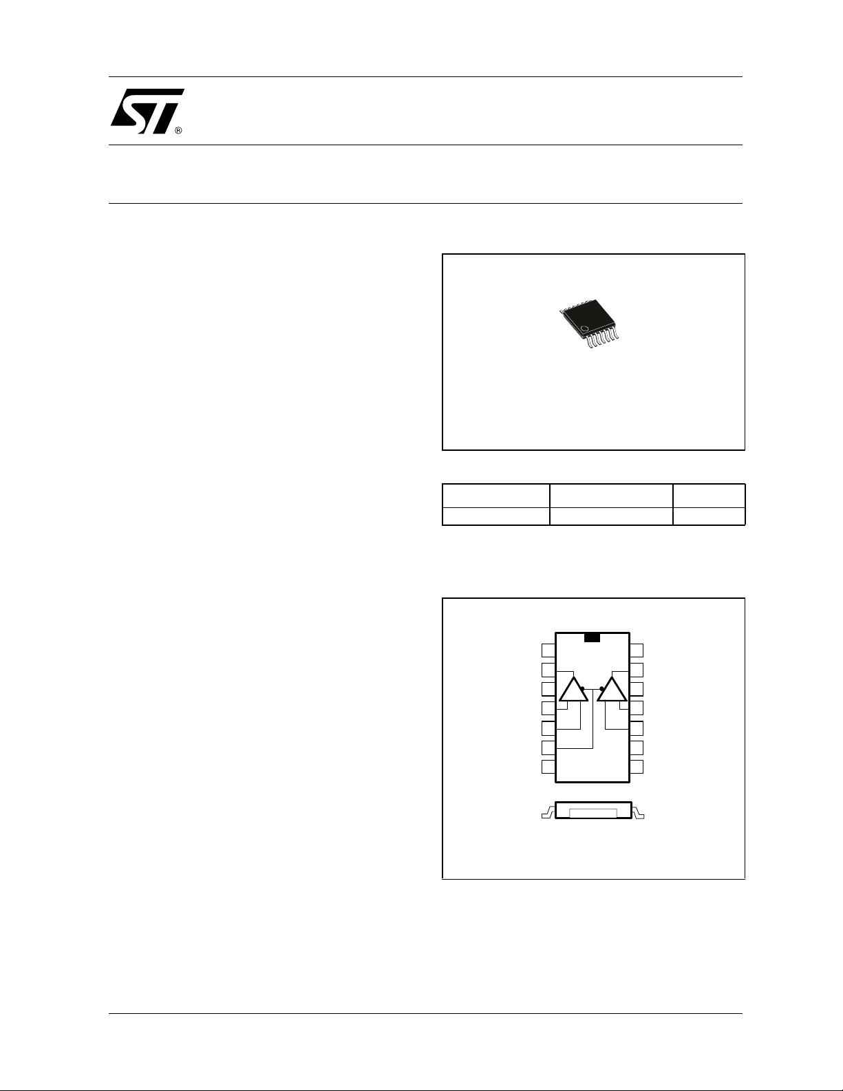
P
TSSOP14 Exposed-Pad
(Plastic Micro package)
ORDER CODE
Part Number Temperature Range Package
TS615IPWT -40, +85°C PW
PW= Thin Shrink Small Outline Package with Exposed-Pad
(TSSOP Exposed-Pad) only available in Tape & Reel (PWT)
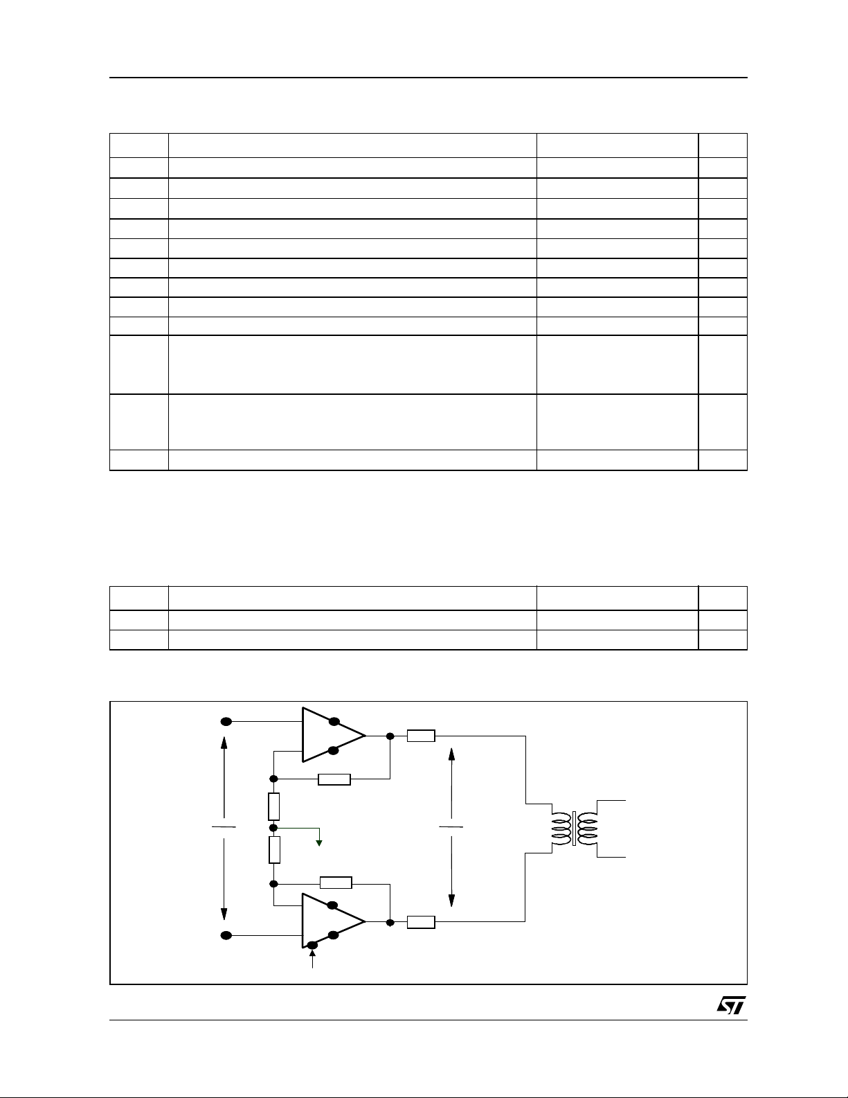
PIN CONNECTIONS (top view)
-VCC1
-VCC1
+VCC1
+VCC1
Non Inverting Input1
Non Inverting Input1
Inverting Input1
Inverting Input1
Power Down
Power Down
NC
NC
1
1
2
2
3
3
+ - - +
+ - - +
4
4
5
5
6
6
7
7
Top View
Top View
14
14
-VCC2
-VCC2
13
13
Output2Output1
Output2Output1
12
12
+VCC2
+VCC2
Non Inverting Input2
Non Inverting Input2
11
11
10
10
Inverting Input2
Inverting Input2
NC
NC
9
9
NC
NC
8
8
APPLICATION
■ Line driver for xDSL
■ Multiple Video Line Driver
December 2002
Cross Section V iew Showi ng Exposed-Pa d
Cross Section V iew Showi ng Exposed-Pa d
This pad c an be con nected to a (-Vcc) copper ar ea on the PCB
This pad c an be con nected to a (-Vcc) copper ar ea on the PCB
1/27
TS615
ABSOLUTE MAXIMUM RATINGS
Symbol Parameter Value Unit
V
T
T
R
R
P
ESD
except
pins 4, 5,
10, 11
ESD
only pins 4,
5, 10, 11
Supply voltage
CC
V
Differential Input Voltage
id
V
in Input Voltage Range
Operating Free Air Temperature Range -40 to + 85 °C
oper
Storage Temperature -65 to +150 °C
std
T
Maximum Junction Temperature 150 °C
j
Thermal Resistance Junction to Case 4 °C/W
thjc
Thermal Resistance Junction to Ambient Area 40 °C/W
thja
Maximum Power Dissipation (@25°C) 3.1 W
max.
CDM : Charged Device Model
HBM : Human Body Model
MM : Machine Model
CDM : Charged Device Model
HBM : Human Body Model
MM : Machine Model
Output Short Circuit
1. All voltage values, except differential voltage are with respect to network terminal.
2. Differential voltage are non-inverting input terminal with respect to the inverting input terminal.
3. The magnitude of input and output voltage must never exceed V
4. An output current limitation protects the circuit from transient currents. Short-circuits can cause excessive heating.
Destructive dissipation can result from short circuit on amplifiers.
1)
2)
3)
±7 V
±2 V
±6 V
1.5
2
200
1
1
100
4)
+0.3V.
CC
kV
kV
V
kV
kV
V
OPERATING CONDITIONS
Symbol Parameter Value Unit
V
V
Power Supply Voltage ±2.5 to ±6 V
CC
+1.5V to +VCC-1.5V
Common Mode Input Voltage
icm
-V
CC
TYPICAL APPLICATION:
Differential Line Driver for xDSL Applications
12
12
11
11
10
10
Vi
Vi
R1
R1
R4
R4
Vi Vo
Vi Vo
5
5
4
4
Pw-Dwn
Pw-Dwn
+
+
1/2TS615
1/2TS615
_
_
14
14
R2
R2
GND
GND
R3
R3
3
3
_
_
1/2TS615
1/2TS615
+
+
1
1
6
6
+Vcc
+Vcc
-Vcc
-Vcc
+Vcc
+Vcc
-Vcc
-Vcc
13
13
2
2
12.5Ω
12.5Ω
12.5Ω
12.5Ω
Vo
Vo
1:2
1:2
25Ω 100Ω
25Ω 100Ω
V
2/27
TS615
ELECTRICAL CHARACTERISTICS
V
= ±6Volts, Rfb=910Ω,T
CC
Note: as described on page 24 (table 71), the TS615 requires a 620Ω feedback res i st or for an optimis ed bandwidth wi t h a gai n of 12 B for
a 12V power supply. Nevertheless, due to production test constraints, the TS615 is tested with the same feedback resistor for 12V and 5V
power su ppl i es (910Ω).
Symbol Parameter Test Condition Min. Typ. Max. Unit
DC PERFORMANCE
V
Input Offset Voltage
io
V
∆
Z
C
CMR
SVR
Differential Input Offset Voltage
io
I
Positive Input Bias Current
ib+
I
Negative Input Bias Current
ib-
Input(+) Impedance 82 k
IN+
Z
Input(-) Impedance 54
IN-
Input(+) Capacitance 1 pF
IN+
Common Mode Rejection Ratio
20 log (∆V
/∆Vio)
ic
Supply Voltage Rejection Ratio
20 log (∆V
I
Total Supply Current per Operator No load 14 17 mA
CC
/∆Vio)
cc
DYNAMIC PERFORMANCE and OUTPUT CHARACTERISTIC
R
Open Loop Transimpedance
OL
-3dB Bandwidth
Full Power Bandwidth
BW
Gain Flatness @ 0.1dB
Tr Rise Time
Tf Fall Time
Ts Settling Time
SR Slew Rate
V
High Level Output Voltage
OH
V
Low Level Output Voltage
OL
Output Sink Current
I
out
Output Source Current
= 25°C (unless otherwise specified)
amb
T
amb
< T
T
min.
T
amb
T
amb
T
min.
T
amb
T
min.
V
∆
ic
T
min.
V
∆
cc
T
min.
V
out
T
min.
< T
amb
= 25°C
< T
< T
amb
< T
< T
amb
= ±4.5V
< T
< T
amb
=±2.5V to ±6V
< T
< T
amb
= 7Vp-p, RL = 25
< T
amb.
Small Signal V
A
= 12dB, RL = 25
V
Large Signal V
= 12dB, RL = 25
A
V
Small Signal V
= 12dB, RL = 25
A
V
V
= 6Vp-p, AV = 12dB, RL
out
= 25
Ω
= 6Vp-p, AV = 12dB, RL
V
out
= 25
Ω
= 6Vp-p, AV = 12dB, RL
V
out
= 25
Ω
= 6Vp-p, AV = 12dB, RL
V
out
= 25
Ω
R
=25Ω Connected to GND
L
R
=25Ω Connected to GND
L
V
= -4Vp
out
< T
T
min.
V
out
T
min.
amb
= +4Vp
< T
amb
< T
< T
< T
max.
max.
max.
max.
max.
max.
<20mVp
out
Ω
=3Vp
out
Ω
<20mVp
out
Ω
max.
max.
1.25 3.5
2.1
mV
2.5 mV
630
7.8
315
3.2
A
µ
A
µ
Ω
Ω
58 63
61
72 79
78
Ω
521
8.9
dB
dB
M
Ω
25 40
MHz
26
7 MHz
10.6 ns
12.2 ns
50 ns
330 410 V/µs
4.8 5.1 V
-5.5 -5.2 V
-350 -530
-440
330 420
mA
365
3/27
TS615
Note: as described on page 24 (table 71), the TS615 requires a 620Ω feedback res i st or for an optimis ed bandwidth wi t h a gai n of 12 B for
a 12V power supply. Nevertheless, due to production test constraints, the TS615 is tested with the same feedback resistor for 12V and 5V
power su ppl i es (910Ω).
Symbol Parameter Test Condition Min. Typ. Max. Unit
NOISE AND DISTORTION
eN Equivalent Input Noise Voltage F = 100kHz 2.5 nV/√Hz
iNp Equivalent Input Noise Current (+) F = 100kHz 15 pA/√Hz
iNn Equivalent Input Noise Current (-) F = 100kHz 21 pA/√Hz
= 14Vp-p, AV = 12dB
HD2
HD3
IM2
IM3
2nd Harmonic distortion
(differential configuration)
3rd Harmonic distortion
(differential configuration)
2nd Order Intermodulation Product
(differential configuration)
3rd Order Intermodulation Produ ct
(differential configuration)
V
out
F= 110kHz, R
= 14Vp-p, AV = 12dB
V
out
F= 110kHz, R
= 50Ω diff.
L
= 50Ω diff.
L
F1= 100kHz, F2 = 110kHz
= 16Vp-p, AV = 12dB
V
out
= 50Ω diff.
R
L
F1= 370kHz, F2 = 400kHz
= 16Vp-p, AV = 12dB
V
out
R
= 50Ω diff.
L
F1 = 100kHz, F2 = 110kHz
= 16Vp-p, AV = 12dB
V
out
= 50Ω diff.
R
L
F1 = 370kHz, F2 = 400kHz
= 16Vp-p, AV = 12dB
V
out
= 50Ω diff.
R
L
-87 dBc
-83 dBc
-76
dBc
-75
-88
dBc
-87
4/27

TS615
ELECTRICAL CHARACTERISTICS
V
= ±2.5Volts, Rfb=910Ω,T
CC
Symbol Parameter Test Condition Min. Typ. Max. Unit
DC PERFORMANCE
V
Input Offset Voltage
io
V
∆
Z
C
CMR
SVR
Differential Input Offset Voltage
io
I
Positive Input Bias Current
ib+
I
Negative Input Bias Current
ib-
Input(+) Impedance 71 k
IN+
Z
Input(-) Impedance 62
IN-
Input(+) Capacitance 1.5 pF
IN+
Common Mode Rejection Ratio
20 log (∆V
/∆Vio)
ic
Supply Voltage Rejection Ratio
20 log (∆V
I
Total Supply Current per Operator No load 11.9 15 mA
CC
/∆Vio)
cc
DYNAMIC PERFORMANCE and OUTPUT CHARACTERISTICS
R
Open Loop Transimpedance
OL
-3dB Bandwidth
BW
Full Power Bandwidth
Gain Flatness @ 0.1dB
Tr Rise Time
Tf Fall Time
Ts Settling Time
SR Slew Rate
V
High Level Output Voltage
OH
V
Low Level Output Voltage
OL
Output Sink Current
I
out
Output Source Current
= 25°C (unless otherwise specified)
amb
T
amb
< T
T
min.
T
amb
T
amb
T
min.
T
amb
T
min.
V
∆
ic
T
min.
V
∆
cc
T
min.
V
out
T
min.
< T
amb
= 25°C
< T
< T
amb
< T
< T
amb
= ±1V
< T
< T
amb.
=±2V to ±2.5V
< T
< T
amb.
= 2Vp-p, RL = 10
< T
< T
amb.
Small Signal V
= 12dB, RL = 10
A
V
Large Signal V
= 12dB, RL = 10
A
V
Small Signal V
A
= 12dB, RL = 10
V
V
= 2.8Vp-p, AV = 12dB
out
= 10
R
Ω
L
V
= 2.8Vp-p, AV = 12dB
out
= 10
R
Ω
L
= 2.2Vp-p, AV = 12dB
V
out
= 10
R
Ω
L
= 2.2Vp-p, AV = 12dB
V
out
R
= 10
Ω
L
R
=10Ω Connected to GND
L
R
=10Ω Connected to GND
L
= -1.25Vp
V
out
< T
T
min.
V
out
T
min.
< T
amb
= +1.25Vp
< T
< T
amb
max.
max.
max.
max.
max.
Ω
max.
<20mVp
out
Ω
= 1.4Vp
out
Ω
<20mVp
out
Ω
max.
max.
0.5 2.5
1.2
2.5 mV
530
8
0.8 11
1.24
55 60
58
63 77
76
25.4
2.1
20 30
MHz
20
5.7 MHz
11 ns
11.5 ns
39 ns
100 130 V/µs
1.5 1.75 V
-2.05 -1.8 V
-350 -470
-450
200 270
245
mV
A
µ
A
µ
Ω
Ω
dB
dB
M
Ω
mA
5/27
TS615
Symbol Parameter Test Condition Min. Typ. Max. Unit
NOISE AND DISTORTION
eN Equivalent Input Noise Voltage F = 100kHz 2.5 nV/√Hz
iNp Equivalent Input Noise Current (+) F = 100kHz 15 pA/√Hz
iNn Equivalent Input Noise Current (-) F = 100kHz 21 pA/√Hz
= 6Vp-p, AV = 12dB
HD2
HD3
IM2
IM3
2nd Harmonic distortion
(differential configuration)
3rd Harmonic distortion
(differential configuration)
2nd Order Intermodulation Product
(differential configuration)
3rd Order Intermodulation Produ ct
(differential configuration)
V
out
F= 110kHz, R
= 6Vp-p, AV = 12dB
V
out
F= 110kHz, R
= 20Ω diff.
L
= 20Ω diff.
L
F1= 100kHz, F2 = 110kHz
= 6Vp-p, AV = 12dB
V
out
R
= 20Ω diff.
L
F1= 370kHz, F2 = 400kHz
V
= 6Vp-p, AV = 12dB
out
= 20Ω diff.
R
L
F1 = 100kHz, F2 = 110kHz
= 6Vp-p, AV = 12dB
V
out
= 20Ω diff.
R
L
F1 = 370kHz, F2 = 400kHz
V
= 6Vp-p, AV = 12dB
out
R
= 20Ω diff.
L
-97 dBc
-98 dBc
-86
-88
-90
-85
dBc
dBc
POWER DOWN MODE FEA TURES (The Power Down command is a MOS input featuring a high input
impedance)
V
= ±2.5Volts, 5Volts, ±6Volts or 12Volts, T
CC
Symbol Parameter Min. Typ. Max. Unit
Pin (6) Threshold Voltage for Power Down Mode
V
Low Level
pdw
High Level
Icc
R
C
Power Down Mode Total Current Consumption@ VCC=5V
pdw
Power Down Mode Total Current Consumption@ V
Power Down Mode Output Impedance @ VCC=5V
pdw
Power Down Mode Output Impedance @ V
Power Down Mode Output Capacitance 63 pF
pdw
POWER DOWN CONTROL CIRCUIT STATUS
V
=Low Level
pdw
=High Level
V
pdw
= 25°C
amb
CC
=12V
CC
Active
Standby
=12V
-V
-V
CC
CC
+2
-VCC+0.8
+V
69 80
148 180
19 23
15.3 19
CC
V
A
µ
A
µ
Ω
Ω
6/27
TS615
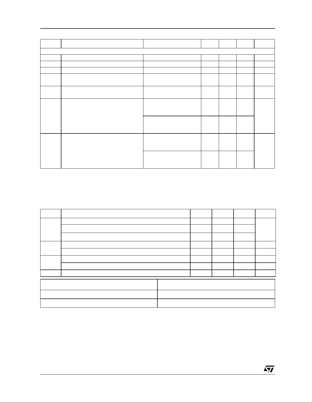
Figure 1 : Load Configuration
Load: RL=25Ω, VCC=±6V
+6V
TS615
TS615
+6V
-6V
-6V
+
+
_
_
25Ω
25Ω
50Ω
50Ω
cable
49.9Ω
49.9Ω
33Ω
33Ω
1W
1W
cable
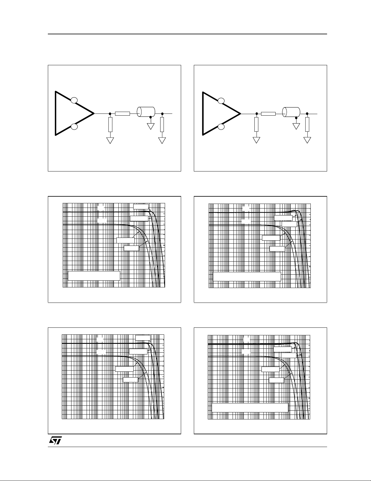
Figure 2 : Closed Loop Gai n vs. Frequency
AV=+1
2
0
-2
-4
-6
-8
(gain (dB)
-10
-12
-14
(Vcc=±2.5V, Rfb=1.1kΩ, Rload=10Ω)
(Vcc=±6V, Rfb=750
-16
100 1k 10k 100k 1M 10M 100M
gain
phase
Ω, Rload=25Ω)
Frequency (Hz)
(Vcc=±6V)
(Vcc=±2.5V)
(Vcc=±2.5V)
(Vcc=±6V)
50Ω
50Ω
40
20
0
-20
-40
-60
-80
-100
-120
Figure 4 : Load Configuration
Load: RL=10Ω, VCC=±2.5V
+2.5V
TS615
TS615
+2.5V
-2.5V
-2.5V
10
10
+
+
_
_
49.9
49.9
Ω
11
11
Ω
Ω
0.5W
0.5W
Ω
Ω
Ω
Figure 5 : Closed Loop Gai n vs. Frequency
AV=-1
2
0
-2
)
°
Phase (
-4
-6
-8
(gain (dB))
-10
-12
-14
(Vcc=±2.5V, Rfb=1kΩ, Rin=1kΩ , Rload=10Ω)
(Vcc=±6V, Rfb=680
-16
100 1k 10k 100k 1M 10M 100M
gain
phase
(Vcc=±2.5V)
(Vcc=±6V)
Ω, Rin=680Ω, Rload=25Ω)
Frequency (Hz)
cable
cable
(Vcc=±2.5V)
(Vcc=±6V)
50
50
Ω
Ω
50
50
Ω
Ω
-140
-160
-180
-200
)
°
-220
Phase (
-240
-260
-280
-300
Figure 3 : Closed Loop Gai n vs. Frequency
AV=+2
8
6
4
2
0
-2
(gain (dB))
-4
-6
-8
-10
100 1k 10k 100k 1M 10M 100M
gain
phase
(Vcc=±2.5V)
Frequency (Hz)
(Vcc=±6V)
(Vcc=±2.5V)
(Vcc=±6V)
40
20
0
-20
-40
-60
-80
-100
-120
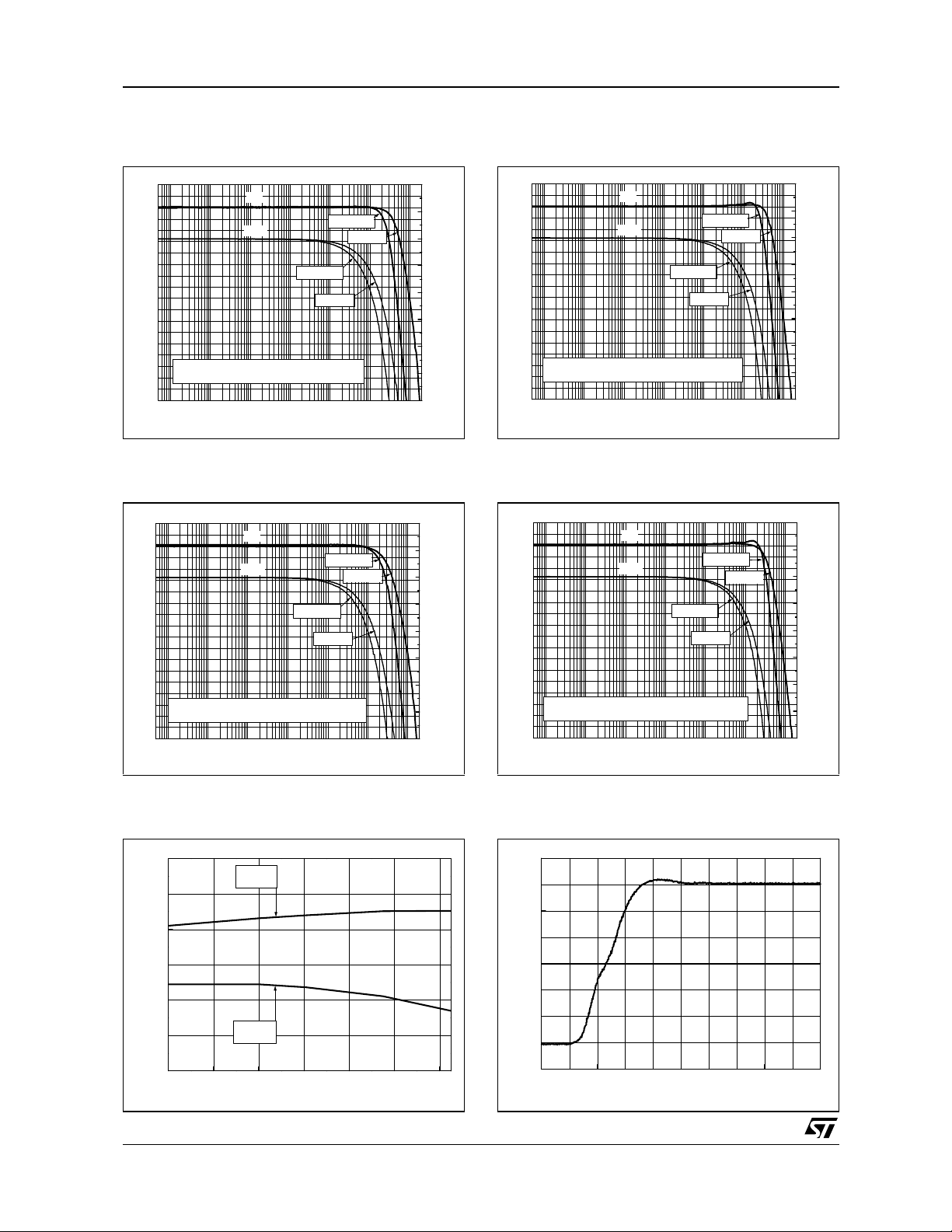
Figure 6 : Closed Loop Gai n vs. Frequency
AV=-2
8
6
4
)
°
Phase (
2
0
-2
(gain (dB))
-4
-6
(Vcc=±2.5V, Rfb=1kΩ, Rin=510Ω, Rload=10Ω)
-8
(Vcc=±6V, Rfb=680
-10
100 1k 10k 100k 1M 10M 100M
gain
phase
(Vcc=±2.5V)
(Vcc=±6V)
Ω, Rin=750//620Ω, Rload=25Ω)
Frequency (Hz)
(Vcc=±2.5V)
(Vcc=±6V)
-140
-160
-180
-200
-220
-240
-260
-280
-300
)
°
Phase (
7/27
TS615
Figure 7 : Closed Loop Gai n vs. Frequency
AV=+4
14
12
10
8
6
4
(gain (dB))
2
0
-2
(Vcc=±2.5V, Rfb=910Ω, Rg=300Ω, Rload=10Ω)
(Vcc=±6V, Rfb=620
-4
100 1k 10k 100k 1M 10M 100M
gain
phase
(Vcc=±2.5V)
(Vcc=±6V)
Ω, R g =560//330Ω, Rload=25Ω)
Frequency (Hz)
(Vcc=±2.5V)
(Vcc=±6V)
Figure 8 : Closed Loop Gai n vs. Frequency
AV=+8
20
18
16
14
12
10
(gain (dB))
8
6
4
(Vcc=±2.5V, Rfb=680Ω, Rg=240//160Ω, Rload=10Ω)
(Vcc=±6V, Rfb=510
2
100 1k 10k 100k 1M 10M 100M
gain
phase
(Vcc=±2.5V)
(Vcc=±6V)
Ω, Rg=270//100Ω, Rload=25Ω)
Frequency (Hz)
(Vcc=±2.5V)
(Vcc=±6V)
40
20
0
-20
-40
-60
-80
-100
-120
40
20
0
-20
-40
-60
-80
-100
-120
Figure 10 : Closed Loop Gain vs. Frequency
AV=-4
14
12
10
8
)
°
Phase (
6
4
(gain (dB))
2
0
(Vcc=±2.5V, Rfb=1kΩ, Rin=320//360Ω, Rload=10Ω)
-2
(Vcc=±6V, Rfb=620
-4
100 1k 10k 100k 1M 10M 100M
gain
phase
(Vcc=±2.5V)
(Vcc=±6V)
Ω, Rin=360//270Ω, Rload=25Ω)
Frequency (Hz)
Figure 11 : Closed Loop Gain vs. Frequency
AV=-8
)
°
Phase (
20
18
16
14
12
10
(gain (dB))
8
6
4
(Vcc=±2.5V, Rfb=680Ω, Rin=160//180Ω, Rload=10Ω)
(Vcc=±6V, Rfb=510
2
100 1k 10k 100k 1M 10M 100M
gain
phase
(Vcc= ± 2. 5V)
(Vcc=±6V)
Ω, Rin=150//110Ω, Rload=25Ω)
Frequency (Hz)
(Vcc=±2.5V)
(Vcc=±6V)
(Vcc=±2.5V)
(Vcc= ± 6V )
-140
-160
-180
-200
-220
-240
-260
-280
-300
-140
-160
-180
-200
-220
-240
-260
-280
-300
)
°
Phase (
)
°
Phase (
Figure 9 : Bandwidth vs. Temperature
AV=+4, Rfb=910
50
45
40
35
Bw (MHz)
30
25
20
-40-200 20406080
8/27
Ω
Vcc=±6V
Load=25
Vcc=±2.5V
Load=10
Ω
Ω
Temperature (°C)
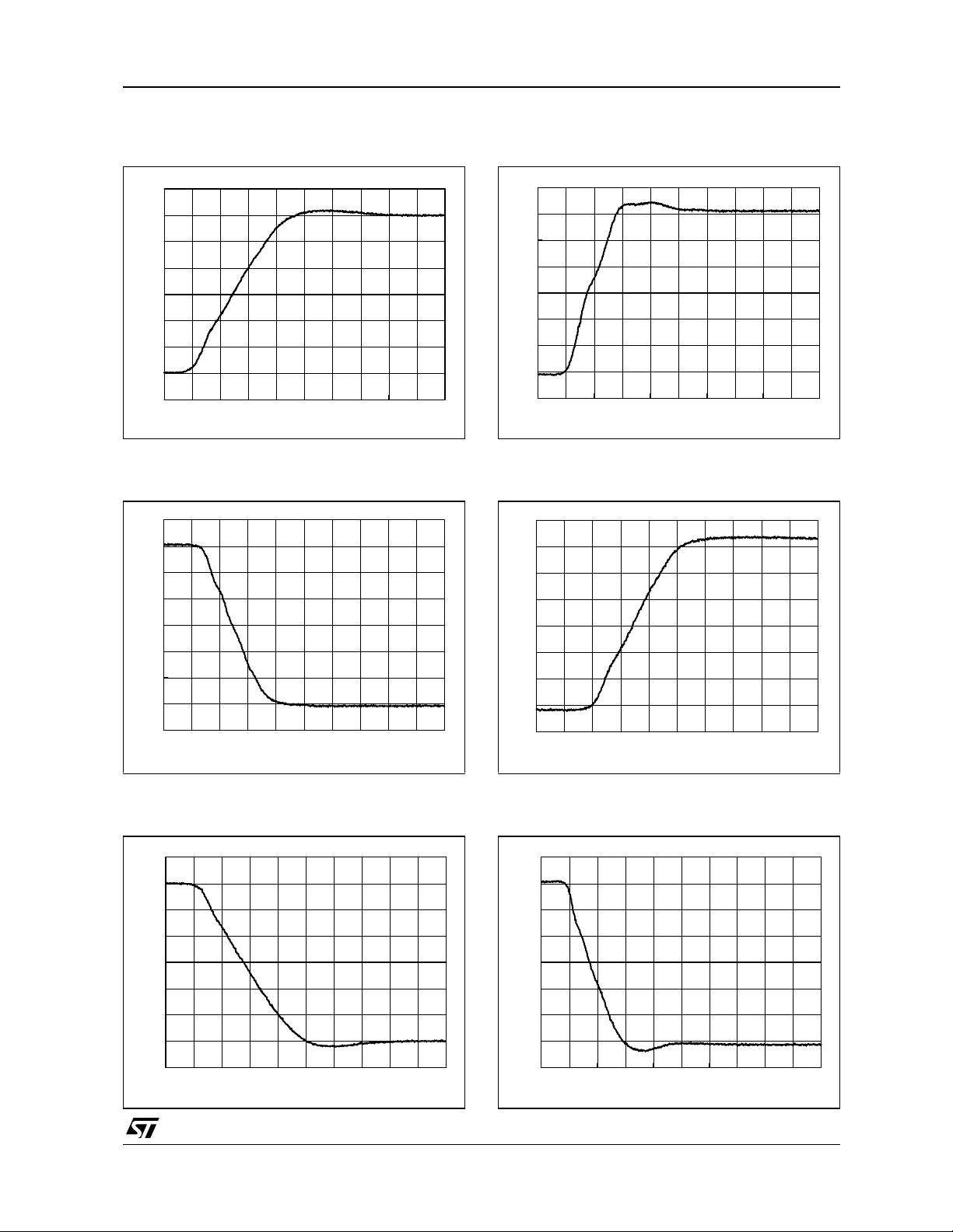
Figure 12 : Positive Slew Rate
AV=+4, Rfb=620
4
2
(V)
0
OUT
V
-2
-4
0.0 10.0n 20.0n 30.0n 40.0n 50.0n
, V
Ω
=±6V, RL=25
CC
Time (s)
Ω
TS615
Figure 13 : Positive Slew Rate
AV=+4, Rfb=910
2
1
(V)
0
OUT
V
-1
-2
0.0 10.0n 20.0n 30.0n 40.0n 50.0n
, V
Ω
CC
=±2.5V, RL=10
Time (s)
Ω
Figure 14 : Negative Slew Rate
AV=+4, Rfb=620Ω, VCC=±6V, RL=25
4
2
Ω
Figure 16 : Positive Slew Rate
AV= - 4, Rfb=620
4
2
(V)
0
OUT
V
-2
-4
0.0 10.0n 20.0n 30.0n 40.0n 50.0n
, V
Ω
=±6V, RL=25
CC
Time (s)
Ω
Figure 17 : Positive Slew Rate
AV= - 4, Rfb=910
2
1
, V
Ω
CC
=±2.5V, RL=10
Ω
(V)
0
OUT
V
-2
-4
0.0 10.0n 20.0n 30.0n 40.0n 50.0n
Time (s)
Figure 15 : Negative Slew Rate
AV=+4, Rfb=910
2
1
(V)
0
OUT
V
-1
-2
0.0 10.0n 20.0n 30.0n 40.0n 50.0n
, V
Ω
CC
=±2.5V, RL=10
Time (s)
Ω
(V)
0
OUT
V
-1
-2
0.0 10.0n 20.0n 30.0n 40.0n 50.0n
Time (s)
Figure 18 : Negative Slew Rate
AV= - 4, Rfb=620Ω, VCC=±6V, RL=25
4
2
(V)
0
OUT
V
-2
-4
0.0 10.0n 20.0n 30.0n 40.0n 50.0n
Time (s)
Ω
9/27
 Loading...