

TS615
DUAL WIDE BAND OPERATIONAL AMPLIFIER
WITH HIGH OUTPUT CURRENT
■ LOW NOISE : 2.5nV/√Hz
■ HIGH OUTPUT CURRENT : 420mA
■ VERY LOW HARMONIC AND INTERMODU-
LATION D I S TORTIO N
■ HIGH SLEW RA TE : 410V/µs
■ -3dB BANDWIDTH : 40MHz@gain=12dB on
25Ω load single ended.
■ 21.2Vp-p DIFFERENTIAL OUTPUT SWING
on 50Ω load, 12V power supply
■ CURRENT FEEDBACK STRUCTURE
■ 5V to 12V POWER SUPPLY
■ SPECIFIED FOR 20Ω and 50Ω DIFFER EN-
TIAL LOAD
■ POWER DOWN FUNCTION WITH A SHORT
CIRCUITED OUTPUT to keep the matching
with the line in sleep mode
DESCRIPTION
The TS615 is a dual operational am plifier featuring a high output current 410mA. These drivers
can be configured differentially for driving signals
in telecommunication systems using multiple carriers. The TS615 is ideally suited for xDSL (High
Speed Asymmetrical Digital Subscriber Line) applications. This circuit is c apable of driving a 10 Ω
or 25Ω load at ±2.5V, 5V, ±6V or +12V power
supply. The TS615 will be able to reach a -3dB
bandwidth of 40MHz on 25Ω load with a 12dB
gain. This device is designed for the high slew
rates to support low harmonic distortion and intermodulation. The TS615 is fitted out with Power
Down function to decrease the consumption. During this sleep state the device displays a short circuit output in order to keep the impedance matching with the line. The TS615 is housed in
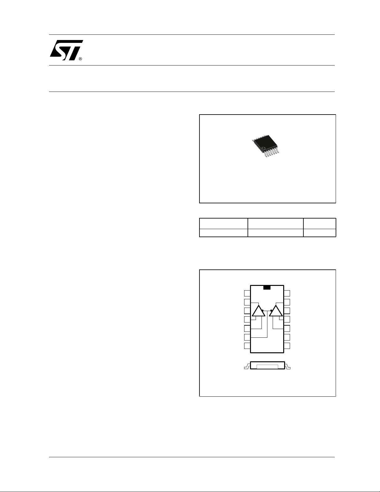
TSSOP14 Exposed-Pad plastic package for a
very low thermal resistance.
P
TSSOP14 Exposed-Pad
(Plastic Micro package)
ORDER CODE
Part Number Temperature Range Package
TS615IPWT -40, +85°C PW
PW= Thin Shrink Small Outline Package with Exposed-Pad
(TSSOP Exposed-Pad) only available in Tape & Reel (PWT)
PIN CONNECTIONS (top view)
-VCC1
-VCC1
+VCC1
+VCC1
Non Inverting Input1
Non Inverting Input1
Inverting Input1
Inverting Input1
Power Down
Power Down
NC
NC
1
1
2
2
3
3
+ - - +
+ - - +
4
4
5
5
6
6
7
7
Top View
Top View
14
14
-VCC2
-VCC2
13
13
Output2Output1
Output2Output1
12
12
+VCC2
+VCC2
Non Inverting Input2
Non Inverting Input2
11
11
10
10
Inverting Input2
Inverting Input2
NC
NC
9
9
NC
NC
8
8
APPLICATION
■ Line driver for xDSL
■ Multiple Video Line Driver
December 2002
Cross Section V iew Showi ng Exposed-Pa d
Cross Section V iew Showi ng Exposed-Pa d
This pad c an be con nected to a (-Vcc) copper ar ea on the PCB
This pad c an be con nected to a (-Vcc) copper ar ea on the PCB
1/27
TS615
ABSOLUTE MAXIMUM RATINGS
Symbol Parameter Value Unit
V
T
T
R
R
P
ESD
except
pins 4, 5,
10, 11
ESD
only pins 4,
5, 10, 11
Supply voltage
CC
V
Differential Input Voltage
id
V
in Input Voltage Range
Operating Free Air Temperature Range -40 to + 85 °C
oper
Storage Temperature -65 to +150 °C
std
T
Maximum Junction Temperature 150 °C
j
Thermal Resistance Junction to Case 4 °C/W
thjc
Thermal Resistance Junction to Ambient Area 40 °C/W
thja
Maximum Power Dissipation (@25°C) 3.1 W
max.
CDM : Charged Device Model
HBM : Human Body Model
MM : Machine Model
CDM : Charged Device Model
HBM : Human Body Model
MM : Machine Model
Output Short Circuit
1. All voltage values, except differential voltage are with respect to network terminal.
2. Differential voltage are non-inverting input terminal with respect to the inverting input terminal.
3. The magnitude of input and output voltage must never exceed V
4. An output current limitation protects the circuit from transient currents. Short-circuits can cause excessive heating.
Destructive dissipation can result from short circuit on amplifiers.
1)
2)
3)
±7 V
±2 V
±6 V
1.5
2
200
1
1
100
4)
+0.3V.
CC
kV
kV
V
kV
kV
V
OPERATING CONDITIONS
Symbol Parameter Value Unit
V
V
Power Supply Voltage ±2.5 to ±6 V
CC
+1.5V to +VCC-1.5V
Common Mode Input Voltage
icm
-V
CC
TYPICAL APPLICATION:
Differential Line Driver for xDSL Applications
12
12
11
11
10
10
Vi
Vi
R1
R1
R4
R4
Vi Vo
Vi Vo
5
5
4
4
Pw-Dwn
Pw-Dwn
+
+
1/2TS615
1/2TS615
_
_
14
14
R2
R2
GND
GND
R3
R3
3
3
_
_
1/2TS615
1/2TS615
+
+
1
1
6
6
+Vcc
+Vcc
-Vcc
-Vcc
+Vcc
+Vcc
-Vcc
-Vcc
13
13
2
2
12.5Ω
12.5Ω
12.5Ω
12.5Ω
Vo
Vo
1:2
1:2
25Ω 100Ω
25Ω 100Ω
V
2/27
TS615
ELECTRICAL CHARACTERISTICS
V
= ±6Volts, Rfb=910Ω,T
CC
Note: as described on page 24 (table 71), the TS615 requires a 620Ω feedback res i st or for an optimis ed bandwidth wi t h a gai n of 12 B for
a 12V power supply. Nevertheless, due to production test constraints, the TS615 is tested with the same feedback resistor for 12V and 5V
power su ppl i es (910Ω).
Symbol Parameter Test Condition Min. Typ. Max. Unit
DC PERFORMANCE
V
Input Offset Voltage
io
V
∆
Z
C
CMR
SVR
Differential Input Offset Voltage
io
I
Positive Input Bias Current
ib+
I
Negative Input Bias Current
ib-
Input(+) Impedance 82 k
IN+
Z
Input(-) Impedance 54
IN-
Input(+) Capacitance 1 pF
IN+
Common Mode Rejection Ratio
20 log (∆V
/∆Vio)
ic
Supply Voltage Rejection Ratio
20 log (∆V
I
Total Supply Current per Operator No load 14 17 mA
CC
/∆Vio)
cc
DYNAMIC PERFORMANCE and OUTPUT CHARACTERISTIC
R
Open Loop Transimpedance
OL
-3dB Bandwidth
Full Power Bandwidth
BW
Gain Flatness @ 0.1dB
Tr Rise Time
Tf Fall Time
Ts Settling Time
SR Slew Rate
V
High Level Output Voltage
OH
V
Low Level Output Voltage
OL
Output Sink Current
I
out
Output Source Current
= 25°C (unless otherwise specified)
amb
T
amb
< T
T
min.
T
amb
T
amb
T
min.
T
amb
T
min.
V
∆
ic
T
min.
V
∆
cc
T
min.
V
out
T
min.
< T
amb
= 25°C
< T
< T
amb
< T
< T
amb
= ±4.5V
< T
< T
amb
=±2.5V to ±6V
< T
< T
amb
= 7Vp-p, RL = 25
< T
amb.
Small Signal V
A
= 12dB, RL = 25
V
Large Signal V
= 12dB, RL = 25
A
V
Small Signal V
= 12dB, RL = 25
A
V
V
= 6Vp-p, AV = 12dB, RL
out
= 25
Ω
= 6Vp-p, AV = 12dB, RL
V
out
= 25
Ω
= 6Vp-p, AV = 12dB, RL
V
out
= 25
Ω
= 6Vp-p, AV = 12dB, RL
V
out
= 25
Ω
R
=25Ω Connected to GND
L
R
=25Ω Connected to GND
L
V
= -4Vp
out
< T
T
min.
V
out
T
min.
amb
= +4Vp
< T
amb
< T
< T
< T
max.
max.
max.
max.
max.
max.
<20mVp
out
Ω
=3Vp
out
Ω
<20mVp
out
Ω
max.
max.
1.25 3.5
2.1
mV
2.5 mV
630
7.8
315
3.2
A
µ
A
µ
Ω
Ω
58 63
61
72 79
78
Ω
521
8.9
dB
dB
M
Ω
25 40
MHz
26
7 MHz
10.6 ns
12.2 ns
50 ns
330 410 V/µs
4.8 5.1 V
-5.5 -5.2 V
-350 -530
-440
330 420
mA
365
3/27
TS615
Note: as described on page 24 (table 71), the TS615 requires a 620Ω feedback res i st or for an optimis ed bandwidth wi t h a gai n of 12 B for
a 12V power supply. Nevertheless, due to production test constraints, the TS615 is tested with the same feedback resistor for 12V and 5V
power su ppl i es (910Ω).
Symbol Parameter Test Condition Min. Typ. Max. Unit
NOISE AND DISTORTION
eN Equivalent Input Noise Voltage F = 100kHz 2.5 nV/√Hz
iNp Equivalent Input Noise Current (+) F = 100kHz 15 pA/√Hz
iNn Equivalent Input Noise Current (-) F = 100kHz 21 pA/√Hz
= 14Vp-p, AV = 12dB
HD2
HD3
IM2
IM3
2nd Harmonic distortion
(differential configuration)
3rd Harmonic distortion
(differential configuration)
2nd Order Intermodulation Product
(differential configuration)
3rd Order Intermodulation Produ ct
(differential configuration)
V
out
F= 110kHz, R
= 14Vp-p, AV = 12dB
V
out
F= 110kHz, R
= 50Ω diff.
L
= 50Ω diff.
L
F1= 100kHz, F2 = 110kHz
= 16Vp-p, AV = 12dB
V
out
= 50Ω diff.
R
L
F1= 370kHz, F2 = 400kHz
= 16Vp-p, AV = 12dB
V
out
R
= 50Ω diff.
L
F1 = 100kHz, F2 = 110kHz
= 16Vp-p, AV = 12dB
V
out
= 50Ω diff.
R
L
F1 = 370kHz, F2 = 400kHz
= 16Vp-p, AV = 12dB
V
out
= 50Ω diff.
R
L
-87 dBc
-83 dBc
-76
dBc
-75
-88
dBc
-87
4/27

TS615
ELECTRICAL CHARACTERISTICS
V
= ±2.5Volts, Rfb=910Ω,T
CC
Symbol Parameter Test Condition Min. Typ. Max. Unit
DC PERFORMANCE
V
Input Offset Voltage
io
V
∆
Z
C
CMR
SVR
Differential Input Offset Voltage
io
I
Positive Input Bias Current
ib+
I
Negative Input Bias Current
ib-
Input(+) Impedance 71 k
IN+
Z
Input(-) Impedance 62
IN-
Input(+) Capacitance 1.5 pF
IN+
Common Mode Rejection Ratio
20 log (∆V
/∆Vio)
ic
Supply Voltage Rejection Ratio
20 log (∆V
I
Total Supply Current per Operator No load 11.9 15 mA
CC
/∆Vio)
cc
DYNAMIC PERFORMANCE and OUTPUT CHARACTERISTICS
R
Open Loop Transimpedance
OL
-3dB Bandwidth
BW
Full Power Bandwidth
Gain Flatness @ 0.1dB
Tr Rise Time
Tf Fall Time
Ts Settling Time
SR Slew Rate
V
High Level Output Voltage
OH
V
Low Level Output Voltage
OL
Output Sink Current
I
out
Output Source Current
= 25°C (unless otherwise specified)
amb
T
amb
< T
T
min.
T
amb
T
amb
T
min.
T
amb
T
min.
V
∆
ic
T
min.
V
∆
cc
T
min.
V
out
T
min.
< T
amb
= 25°C
< T
< T
amb
< T
< T
amb
= ±1V
< T
< T
amb.
=±2V to ±2.5V
< T
< T
amb.
= 2Vp-p, RL = 10
< T
< T
amb.
Small Signal V
= 12dB, RL = 10
A
V
Large Signal V
= 12dB, RL = 10
A
V
Small Signal V
A
= 12dB, RL = 10
V
V
= 2.8Vp-p, AV = 12dB
out
= 10
R
Ω
L
V
= 2.8Vp-p, AV = 12dB
out
= 10
R
Ω
L
= 2.2Vp-p, AV = 12dB
V
out
= 10
R
Ω
L
= 2.2Vp-p, AV = 12dB
V
out
R
= 10
Ω
L
R
=10Ω Connected to GND
L
R
=10Ω Connected to GND
L
= -1.25Vp
V
out
< T
T
min.
V
out
T
min.
< T
amb
= +1.25Vp
< T
< T
amb
max.
max.
max.
max.
max.
Ω
max.
<20mVp
out
Ω
= 1.4Vp
out
Ω
<20mVp
out
Ω
max.
max.
0.5 2.5
1.2
2.5 mV
530
8
0.8 11
1.24
55 60
58
63 77
76
25.4
2.1
20 30
MHz
20
5.7 MHz
11 ns
11.5 ns
39 ns
100 130 V/µs
1.5 1.75 V
-2.05 -1.8 V
-350 -470
-450
200 270
245
mV
A
µ
A
µ
Ω
Ω
dB
dB
M
Ω
mA
5/27
TS615
Symbol Parameter Test Condition Min. Typ. Max. Unit
NOISE AND DISTORTION
eN Equivalent Input Noise Voltage F = 100kHz 2.5 nV/√Hz
iNp Equivalent Input Noise Current (+) F = 100kHz 15 pA/√Hz
iNn Equivalent Input Noise Current (-) F = 100kHz 21 pA/√Hz
= 6Vp-p, AV = 12dB
HD2
HD3
IM2
IM3
2nd Harmonic distortion
(differential configuration)
3rd Harmonic distortion
(differential configuration)
2nd Order Intermodulation Product
(differential configuration)
3rd Order Intermodulation Produ ct
(differential configuration)
V
out
F= 110kHz, R
= 6Vp-p, AV = 12dB
V
out
F= 110kHz, R
= 20Ω diff.
L
= 20Ω diff.
L
F1= 100kHz, F2 = 110kHz
= 6Vp-p, AV = 12dB
V
out
R
= 20Ω diff.
L
F1= 370kHz, F2 = 400kHz
V
= 6Vp-p, AV = 12dB
out
= 20Ω diff.
R
L
F1 = 100kHz, F2 = 110kHz
= 6Vp-p, AV = 12dB
V
out
= 20Ω diff.
R
L
F1 = 370kHz, F2 = 400kHz
V
= 6Vp-p, AV = 12dB
out
R
= 20Ω diff.
L
-97 dBc
-98 dBc
-86
-88
-90
-85
dBc
dBc
POWER DOWN MODE FEA TURES (The Power Down command is a MOS input featuring a high input
impedance)
V
= ±2.5Volts, 5Volts, ±6Volts or 12Volts, T
CC
Symbol Parameter Min. Typ. Max. Unit
Pin (6) Threshold Voltage for Power Down Mode
V
Low Level
pdw
High Level
Icc
R
C
Power Down Mode Total Current Consumption@ VCC=5V
pdw
Power Down Mode Total Current Consumption@ V
Power Down Mode Output Impedance @ VCC=5V
pdw
Power Down Mode Output Impedance @ V
Power Down Mode Output Capacitance 63 pF
pdw
POWER DOWN CONTROL CIRCUIT STATUS
V
=Low Level
pdw
=High Level
V
pdw
= 25°C
amb
CC
=12V
CC
Active
Standby
=12V
-V
-V
CC
CC
+2
-VCC+0.8
+V
69 80
148 180
19 23
15.3 19
CC
V
A
µ
A
µ
Ω
Ω
6/27
TS615
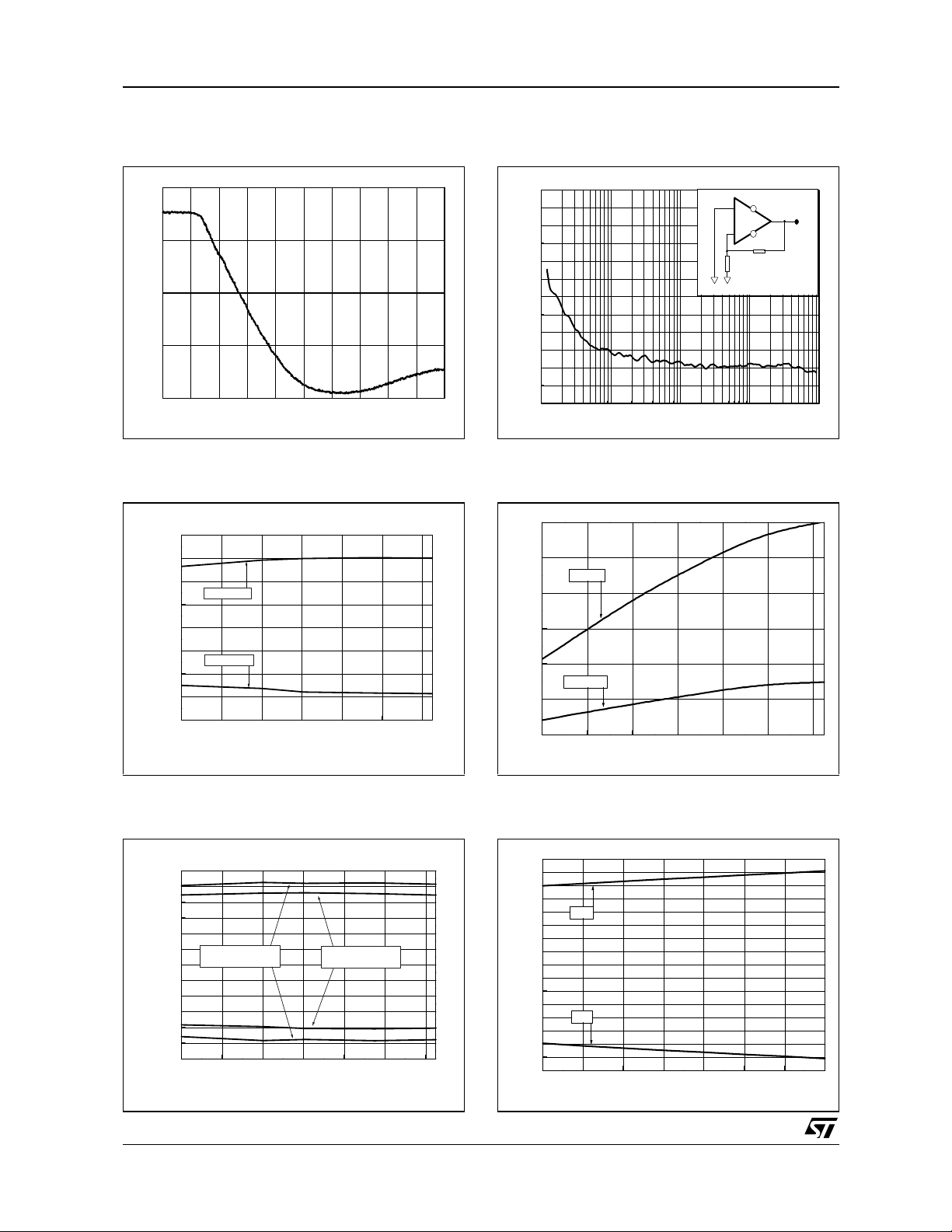
Figure 1 : Load Configuration
Load: RL=25Ω, VCC=±6V
+6V
TS615
TS615
+6V
-6V
-6V
+
+
_
_
25Ω
25Ω
50Ω
50Ω
cable
49.9Ω
49.9Ω
33Ω
33Ω
1W
1W
cable
Figure 2 : Closed Loop Gai n vs. Frequency
AV=+1
2
0
-2
-4
-6
-8
(gain (dB)
-10
-12
-14
(Vcc=±2.5V, Rfb=1.1kΩ, Rload=10Ω)
(Vcc=±6V, Rfb=750
-16
100 1k 10k 100k 1M 10M 100M
gain
phase
Ω, Rload=25Ω)
Frequency (Hz)
(Vcc=±6V)
(Vcc=±2.5V)
(Vcc=±2.5V)
(Vcc=±6V)
50Ω
50Ω
40
20
0
-20
-40
-60
-80
-100
-120
Figure 4 : Load Configuration
Load: RL=10Ω, VCC=±2.5V
+2.5V
TS615
TS615
+2.5V
-2.5V
-2.5V
10
10
+
+
_
_
49.9
49.9
Ω
11
11
Ω
Ω
0.5W
0.5W
Ω
Ω
Ω
Figure 5 : Closed Loop Gai n vs. Frequency
AV=-1
2
0
-2
)
°
Phase (
-4
-6
-8
(gain (dB))
-10
-12
-14
(Vcc=±2.5V, Rfb=1kΩ, Rin=1kΩ , Rload=10Ω)
(Vcc=±6V, Rfb=680
-16
100 1k 10k 100k 1M 10M 100M
gain
phase
(Vcc=±2.5V)
(Vcc=±6V)
Ω, Rin=680Ω, Rload=25Ω)
Frequency (Hz)
cable
cable
(Vcc=±2.5V)
(Vcc=±6V)
50
50
Ω
Ω
50
50
Ω
Ω
-140
-160
-180
-200
)
°
-220
Phase (
-240
-260
-280
-300
Figure 3 : Closed Loop Gai n vs. Frequency
AV=+2
8
6
4
2
0
-2
(gain (dB))
-4
-6
-8
-10
100 1k 10k 100k 1M 10M 100M
gain
phase
(Vcc=±2.5V)
Frequency (Hz)
(Vcc=±6V)
(Vcc=±2.5V)
(Vcc=±6V)
40
20
0
-20
-40
-60
-80
-100
-120
Figure 6 : Closed Loop Gai n vs. Frequency
AV=-2
8
6
4
)
°
Phase (
2
0
-2
(gain (dB))
-4
-6
(Vcc=±2.5V, Rfb=1kΩ, Rin=510Ω, Rload=10Ω)
-8
(Vcc=±6V, Rfb=680
-10
100 1k 10k 100k 1M 10M 100M
gain
phase
(Vcc=±2.5V)
(Vcc=±6V)
Ω, Rin=750//620Ω, Rload=25Ω)
Frequency (Hz)
(Vcc=±2.5V)
(Vcc=±6V)
-140
-160
-180
-200
-220
-240
-260
-280
-300
)
°
Phase (
7/27
TS615
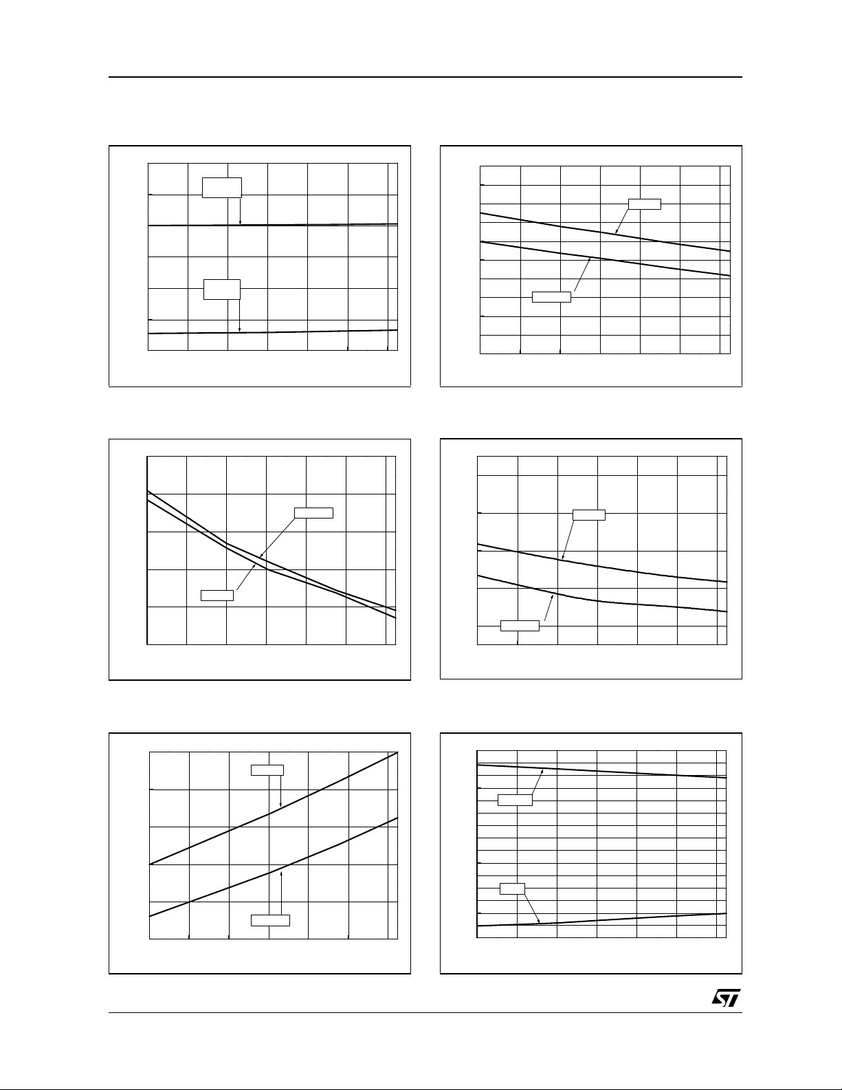
Figure 7 : Closed Loop Gai n vs. Frequency
AV=+4
14
12
10
8
6
4
(gain (dB))
2
0
-2
(Vcc=±2.5V, Rfb=910Ω, Rg=300Ω, Rload=10Ω)
(Vcc=±6V, Rfb=620
-4
100 1k 10k 100k 1M 10M 100M
gain
phase
(Vcc=±2.5V)
(Vcc=±6V)
Ω, R g =560//330Ω, Rload=25Ω)
Frequency (Hz)
(Vcc=±2.5V)
(Vcc=±6V)
Figure 8 : Closed Loop Gai n vs. Frequency
AV=+8
20
18
16
14
12
10
(gain (dB))
8
6
4
(Vcc=±2.5V, Rfb=680Ω, Rg=240//160Ω, Rload=10Ω)
(Vcc=±6V, Rfb=510
2
100 1k 10k 100k 1M 10M 100M
gain
phase
(Vcc=±2.5V)
(Vcc=±6V)
Ω, Rg=270//100Ω, Rload=25Ω)
Frequency (Hz)
(Vcc=±2.5V)
(Vcc=±6V)
40
20
0
-20
-40
-60
-80
-100
-120
40
20
0
-20
-40
-60
-80
-100
-120
Figure 10 : Closed Loop Gain vs. Frequency
AV=-4
14
12
10
8
)
°
Phase (
6
4
(gain (dB))
2
0
(Vcc=±2.5V, Rfb=1kΩ, Rin=320//360Ω, Rload=10Ω)
-2
(Vcc=±6V, Rfb=620
-4
100 1k 10k 100k 1M 10M 100M
gain
phase
(Vcc=±2.5V)
(Vcc=±6V)
Ω, Rin=360//270Ω, Rload=25Ω)
Frequency (Hz)
Figure 11 : Closed Loop Gain vs. Frequency
AV=-8
)
°
Phase (
20
18
16
14
12
10
(gain (dB))
8
6
4
(Vcc=±2.5V, Rfb=680Ω, Rin=160//180Ω, Rload=10Ω)
(Vcc=±6V, Rfb=510
2
100 1k 10k 100k 1M 10M 100M
gain
phase
(Vcc= ± 2. 5V)
(Vcc=±6V)
Ω, Rin=150//110Ω, Rload=25Ω)
Frequency (Hz)
(Vcc=±2.5V)
(Vcc=±6V)
(Vcc=±2.5V)
(Vcc= ± 6V )
-140
-160
-180
-200
-220
-240
-260
-280
-300
-140
-160
-180
-200
-220
-240
-260
-280
-300
)
°
Phase (
)
°
Phase (
Figure 9 : Bandwidth vs. Temperature
AV=+4, Rfb=910
50
45
40
35
Bw (MHz)
30
25
20
-40-200 20406080
8/27
Ω
Vcc=±6V
Load=25
Vcc=±2.5V
Load=10
Ω
Ω
Temperature (°C)
Figure 12 : Positive Slew Rate
AV=+4, Rfb=620
4
2
(V)
0
OUT
V
-2
-4
0.0 10.0n 20.0n 30.0n 40.0n 50.0n
, V
Ω
=±6V, RL=25
CC
Time (s)
Ω
TS615
Figure 13 : Positive Slew Rate
AV=+4, Rfb=910
2
1
(V)
0
OUT
V
-1
-2
0.0 10.0n 20.0n 30.0n 40.0n 50.0n
, V
Ω
CC
=±2.5V, RL=10
Time (s)
Ω
Figure 14 : Negative Slew Rate
AV=+4, Rfb=620Ω, VCC=±6V, RL=25
4
2
Ω
Figure 16 : Positive Slew Rate
AV= - 4, Rfb=620
4
2
(V)
0
OUT
V
-2
-4
0.0 10.0n 20.0n 30.0n 40.0n 50.0n
, V
Ω
=±6V, RL=25
CC
Time (s)
Ω
Figure 17 : Positive Slew Rate
AV= - 4, Rfb=910
2
1
, V
Ω
CC
=±2.5V, RL=10
Ω
(V)
0
OUT
V
-2
-4
0.0 10.0n 20.0n 30.0n 40.0n 50.0n
Time (s)
Figure 15 : Negative Slew Rate
AV=+4, Rfb=910
2
1
(V)
0
OUT
V
-1
-2
0.0 10.0n 20.0n 30.0n 40.0n 50.0n
, V
Ω
CC
=±2.5V, RL=10
Time (s)
Ω
(V)
0
OUT
V
-1
-2
0.0 10.0n 20.0n 30.0n 40.0n 50.0n
Time (s)
Figure 18 : Negative Slew Rate
AV= - 4, Rfb=620Ω, VCC=±6V, RL=25
4
2
(V)
0
OUT
V
-2
-4
0.0 10.0n 20.0n 30.0n 40.0n 50.0n
Time (s)
Ω
9/27
TS615
Figure 19 : Negative Slew Rate
AV= - 4, Rfb=910
2
(V)
0
OUT
V
-2
0.0 10.0n 20.0n 30.0n 40.0n 50.0n
, V
Ω
CC
=±2.5V, RL=10
Time (s)
Ω
Figure 20 : Slew Rate vs. Temperature
AV=+4, Rfb=910
200
150
100
s)
µ
50
0
−50
Slew Rate (V/
−100
−150
−200
−40 −200 20406080
, V
Ω
Positive SR
Negative SR
=±2.5V, RL=10
CC
Temperature (°C)
Ω
Figure 22 : Input Voltage Noise Level
AV=+92, Rfb=910Ω, Input+ connected to Gnd via 10
5.0
+ 6V
+ 6V
+ 6V
+ 6V
+
+
+
+
Output
Output
Output
4.5
Hz)
√
4.0
3.5
3.0
Input Voltage Noise (nV/
2.5
2.0
100 1k 10k 100k 1M
10
10
10
10
(Frequency (Hz)
Output
_
_
_
_
6VΩ-
6VΩ-
- 6V
- 6V
910Ω
910
910Ω
910
Ω
Ω
Ω
Ω
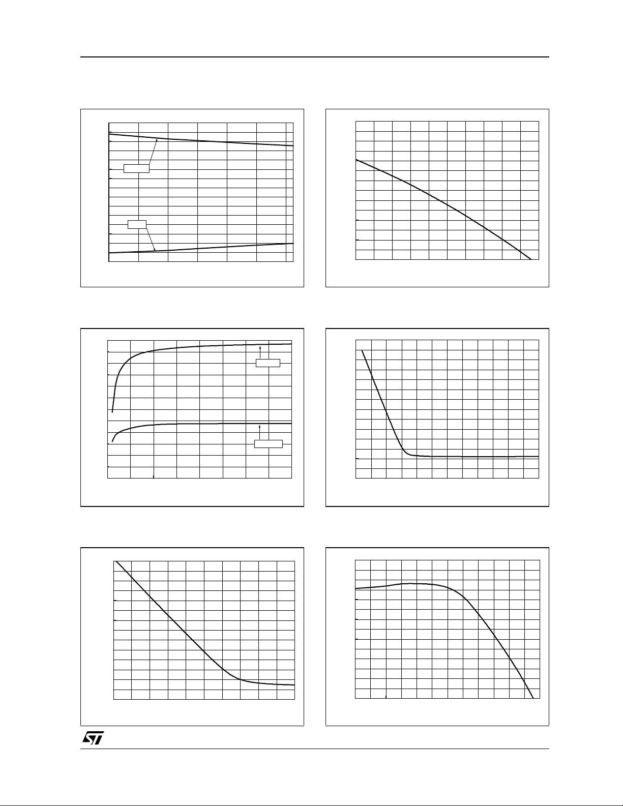
Figure 23 : Transimpedance vs. Temperature
Open Loop
)
Ω
(M
R
30
25
Vcc=±6V
20
15
OL
10
Vcc=±2.5V
5
0
-40-200 20406080
Temperature (°C)
Ω
Figure 21 : Slew Rate vs. Temperature
AV=+4, Rfb=910
600
500
400
300
200
s)
µ
100
0
−100
−200
Slew Rate (V/
−300
−400
−500
−600
−40 −200 20406080
10/27
, V
=±6V, RL=25
Ω
CC
Positive&Negative SR
Ω
Rfb=620
Temperature (°C)
Ω
Positive&Negative SR
Ω
Rfb=910
Figure 24 : Icc vs. Power Supply
Open loop, no load
16
14
12
10
8
Icc(+)
6
4
2
0
(mA)
-2
CC
I
-4
-6
Icc(-)
-8
-10
-12
-14
-16
56789101112
VCC (V)

TS615
Figure 25 : Iib vs. Power Supply
Open loop, no load
7
IB+
6
5
4
A)
µ
(
B
3
I
IB-
2
1
0
5 6 7 8 9 10 11 12
Vcc (V)
Figure 26 : I
Open loop, no load
5
4
3
A)
µ
(
IB(-)
2
I
1
0
-40-200 20406080
ib(-) vs. Temperature
Vcc=±6V
Vcc=±2.5V
Temper ature (°C)
Figure 28 : I
ib(+) vs. Temper ature
Open loop, no load
8
7
6
5
4
A)
µ
(
3
IB(+)
I
2
1
0
-1
-40-200 20406080
Figure 29 : V
Open loop, RL=25
6
5
4
3
2
(V)
1
OL
0
& V
-1
OH
V
-2
-3
-4
-5
-6
56789101112
Vcc=±6V
Vcc=±2.5V
Temperature (° C)
oh & Vol vs. Power Supply
Ω
VOH
VOL
Vcc (V)
Figure 27 : I
cc vs. Temperature
Open loop, no load
14
12
10
Icc(+) for Vcc=±2.5V
8
Icc(+) for Vcc=±6V
6
4
2
0
(mA)
-2
CC
I
-4
-6
Icc(-) for Vcc=±6V
-8
-10
-12
-14
Icc(-) for Vcc=±2.5V
-40-200 20406080
Tem perature ( °C)
Figure 30 : V
oh vs. Temperature
Open loop
6
5
4
3
(V)
OH
V
2
1
0
-40-200 20406080
Vcc=±6vV
Ω
Load=25
Vcc=±2.5V
Ω
Load=10
Temperature (°C)
11/27
TS615
Figure 31 : Vol vs. Temperature
Open loop
0
Vcc=±2.5V
Load=10
-1
-2
-3
(V)
OL
V
-4
-5
-6
-40-200 20406080
Figure 32 : Differential V
Open loop, no load
450
400
350
V)
µ
(
IO
V
∆
300
250
200
-40-200 20406080
Ω
Vcc=±6V
Load=25
Ω
Temperature (°C)
Vcc=±6V
Temperature (°C)
io vs. Temperature
Vcc=±2.5V
Figure 34 : CMR vs. Temperature
Open loop, no load
70
68
66
64
62
60
58
CMR (dB)
56
54
52
50
-40-200 20406080
Vcc=±2.5V
Temperature (°C)
Vcc=±6V
Figure 35 : SVR vs. Temperature
Open loop, no load
84
82
80
SVR (dB)
78
76
Vcc=±2.5V
-40-200 20406080
Vcc=±6V
Temperature (°C)
Figure 33 : V
io vs. Temperature
Open loop, no load
2.0
Vcc=±6V
1.5
1.0
(mV)
IO
V
0.5
0.0
Vcc=±2.5V
-0.5
-40-20 0 20406080
Temperature (°C)
12/27
Figure 36 : Iout vs. Temperature
Open loop, VCC=±6V, RL=10Ω
300
250
200
150
100
Isource
50
0
-50
-100
-150
Iout (mA)
-200
-250
-300
-350
-400
-450
Isink
-40-200 20406080
Temperature (°C)
TS615
Figure 37 : Iout vs. Temperature
Open loop, VCC=±2.5V, RL=25Ω
300
250
200
150
100
50
Isource
0
-50
-100
-150
Iout (mA)
-200
-250
-300
-350
-400
-450
Isink
-40-200 20406080
Temperature (°C)
Figure 38 : Maximum Output Amplitude vs. Load
AV=+4, Rfb=620Ω, VCC=±6V
12
)
(V
V
10
8
P-P
6
OUT-MAX
4
2
Vcc=±6V
Vcc=±2.5V
Figure 40 : Isource vs. Output Amplitude.
VCC=±2.5V, Open Loop, no Load
700
600
500
400
300
Isource (mA)
200
100
0
0.0 0.5 1.0 1.5 2.0 2.5
Vout (V)
Figure 41 : Isink vs. Output Amplitude
VCC=±6V, Open Loop, no Load
0
-100
-200
-300
-400
Isink (mA)
-500
-600
0
0 50 100 150 200
R
(Ω)
LOAD
Figure 39 : Isink vs. Output Amplitude.
VCC=±2.5V, Open Loop, no Load
0
-100
-200
-300
-400
Isink (mA)
-500
-600
-700
-2.5 -2.0 -1.5 -1.0 -0.5 0.0
Vou t (V)
-700
-6 -5 -4 -3 -2 -1 0
Vout (V)
Figure 42 : Isource vs. Output Amplitude
VCC=±6V, Open Loop, no Load
700
600
500
400
300
Isource (mA)
200
100
0
0123456
Vout (V)
13/27

TS615
Figure 43 : Icc (Power Down) vs. Temperature
No load, Open Loop
200
150
100
50
A)
µ
0
(
CC pdw
-50
I
-100
-150
-200
Vcc=±2.5V
-40-200 20406080
Vcc=±6V
Temperature (°C)
Figure 44 : Group Delay
VCC=±6V, VCC=±2.5V
100
90
80
70
60
50
Delay (ns)
40
30
20
10
300k
1M 10M
Frequency (Hz)
Av=4
Vcc=±6V, Rfb=620Ω, Load = 25Ω
Vcc=±2.5V, R f b=910Ω, Load =10Ω
IF Bw = 10Hz
Smoothing=19.247MHz
on 10ns/div scale
50M
14/27

TS615
C
t
INTERMODULATION DISTORTION PRODUCT
A non-ideal output of the amplifier can be described by the following development :
Vout C0C1VinC2V
++ +=
2
in
…
CnV
n
in
due to a non-linearity in the input-output amplitude
transfer. In the case of the input is Vin=Asinωt, C
is the DC component, C1(Vin) is the fundamental,
C
is the amplitude of the harmonics of the output
n
signal V
out
.
A one-frequency (one-tone) input signal contributes to a harmonic distortion. A two-tones input
signal contributes to a harmonic disto rtion and intermodulation product.
This intermodulation product or intermodulation
distortion study of a two-tones input signal is the
first step of the amplifier characterization of driving
capability in the case of a multi-tone signal.
In this case :
C
+A
()
2
C
+
…
()
n
VinA
tsin B
ω
1
A
tsin B
ω
1
tsin B
ω
1
2
tsin+
ω
2
n
tsin+
ω
2
tsin+=
ω
2
In this expression, we recognize the second order
intermodulation IM2 by the frequencies (ω
and (ω
IM3 by the frequencies (2ω
+2ω2) and (ω1+2ω2).
(−ω
1
) and the third order intermodulation
1+ω2
), (2ω1+ω2),
1-ω2
The measurement of the intermodulation product
of the driver is achieved by using the driver as a
0
mixer by a summing amplifier configuration. By
this way, the non-linearity problem of an external
mixing device is avoided.
Figure 45 : Non-inve r t ing S umming Amp lif ier
1kΩ
1kΩ
1kΩ
1kΩ
49.9Ω
Vin1
Vin1
50Ω
50Ω
1:√2
1:√2
North Hills
North Hills
0315PB
0315PB
400Ω
400Ω
Vin2
Vin2
50Ω
50Ω
49.9Ω
1:√2
1:√2
North Hills
North Hills
0315PB
0315PB
49.9Ω
49.9Ω
400Ω
400Ω
49.9Ω
49.9Ω
49.9Ω
49.9Ω
1kΩ
1kΩ
11
11
+Vcc
+Vcc
+
+
1/2TS615
1/2TS615
_
_
13
13
10
10
Rfb1
Rfb1
Rg1
Rg1
Vout diff.
Vout diff.
Rg2
Rg2
Rfb2
Rfb2
_
_
1/2TS615
1/2TS615
1kΩ
1kΩ
+
+
-Vcc
-Vcc
33
33
33Ω
33Ω
49.9Ω
49.9Ω
49.9Ω
49.9Ω
Ω
Ω
1-ω2
√2:1
√2:1
100Ω 50Ω
100Ω 50Ω
North Hills
North Hills
0315PB
0315PB
)
V
outC0C1
+=
and :
C+
()
1
C
2
2
------- A
–
2+C2AB
3C3A2B
----------------------- -+2
2
3C3A2B
----------------------- -+
2
3
A
tsi n B
ω
1
cos t B
2
()
C3A33
+
()
–
()
…
V
outC0C2
3
ω
A
()
A
ω
2
ω
1
–
ω1ω
()
3
ω
–
ω
1
ω
1
C
+
+=
t2A2B
2
tsin B
ω
1
tsin B
1
ω
2
t
cos– tcos
2
3
-------
¥+
4
tsin B33
1
1
tsin
-- -– 2
ω
2
2
1
–
2ω+
tsin
-- 2
2
n
V
()
n
in
A2B2+
---------------------
2
ω
tsin+
ω
2
tsin+
2
2
tcos+
ω
2
–
ω
ω
()
1
2
tsin+
ω
2
+
ω1ω
()
ω
()
1
tsin 2AB
1
tsin
2
2ω+
tsin
2
2
ω
sin++sin+
2
The following graphs show the IM2 and the IM3 of
the amplifier in different configuration. The
two-tones input signal is achieved by the multisource generator Marconi 2026. Each tone has
the same amplitude. The measurement is
achieved by the spectrum analyzer HP3585A .
15/27

TS615
Figure 46 : Intermodulation vs. Output Amplitude
370kHz & 400kHz, AV=+1.5, Rfb=1kΩ, RL=14Ω diff.,VCC=±2.5V
IM2
30kHz
IM3
1140kHz, 1170kHz
-30
-40
-50
-60
IM3
-70
340kHz, 430kHz
-80
IM2 and IM3 (dBc)
-90
-100
012345678
IM2
770kHz
Differential Output Voltage (Vp-p)
Figure 47 : Intermodulation vs. Output Amplitude
370kHz & 400kHz, AV=+1.5, Rfb=1kΩ, RL=28Ω diff.,VCC=±2.5V
IM2
30kHz
IM2
770kHz
IM3
1140kHz, 1170kHz
-30
-40
-50
-60
IM3
340kHz, 430kHz
-70
-80
IM2 and IM3 (dBc)
-90
-100
012345678
Differential Output Voltage (Vp-p)
Figure 49 : Intermodulation vs. Load
370kHz & 400kHz, AV=+1.5, Rfb=1kΩ, Vout=6.5Vpp, VCC=±2.5V
-30
-40
-50
-60
-70
-80
IM2 and IM3 (dBc)
-90
-100
-110
0 20 40 60 80 100 120 140 160 180 200
IM3
340kHz, 430kHz, 1140kHz, 1170kHz
IM2
30kHz
IM2
770kHz
Differential Load (Ω)
Figure 50 : Intermodulation vs. Output Amplitude
100kHz & 110kHz, AV=+4, Rfb=620Ω, RL=200Ω diff.,VCC=±6V
IM3
320kHz
IM2
210kHz
-30
-40
-50
IM3
90kHz, 120kHz
-60
-70
-80
IM2 and IM3 (dBc)
-90
-100
-110
246810121416182022
IM3
310kHz
Differential Output Voltage (Vp-p)
Figure 48 : Intermodulation vs. Gain
370kHz & 400kHz, RL=20Ω diff., Vout=6Vpp, VCC=±2.5V
-30
-40
-50
-60
-70
-80
IM2 and IM3 (dBc)
-90
-100
-110
1.0 1.5 2.0 2.5 3.0 3.5 4.0
IM3
340kHz, 430kHz, 1140kHz, 1170kHz
IM2
30kHz
Closed Lo op Gain (Linear)
16/27
IM2
770kHz
Figure 51 : Intermodulation vs. Output Amplitude
100kHz & 110kHz, AV=+4, Rfb=620Ω, RL=50Ω diff., VCC=±6V
-30
-40
-50
-60
-70
-80
IM2 and IM3 (dBc)
-90
-100
-110
2 4 6 8 10121416182022
IM3
90kHz, 120kHz, 310kHz, 320kHz
Differential Output Voltage (Vp -p)
IM2
210kHz

TS615
Figure 52 : Intermodulation vs. Frequency Range
AV=+4, Rfb=620Ω, RL=50Ω diff., Vout=16Vp p, VCC=±6V
f1=400kHz
f2=430kHz
f1=1MHz
f2=1.1MHz
1.1M
-60
Quadratic Summation of all IM2 and IM3 components
generated by each two-tones signal
-65
-70
f1=100kHz
-75
f2=110kHz
-80
(dB)
-85
-90
-95
-100
f1=200kHz
f2=230kHz
100k 200k 300k 400k 500k 600k 700k 800k 900k 1M 1M
Frequency (Hz)
Figure 53 : Intermodulation vs. Output Amplitude
370kHz & 400kHz, AV=+4, Rfb=620Ω, RL=200Ω diff.,VCC=±6V
-30
-40
-50
-60
-70
IM3
-80
340kHz, 430kHz
IM2 and IM3 (dBc)
-90
IM3
1140kHz, 1170kHz
IM2
770kHz
IM2
30kHz
Figure 54 : Intermodulation vs. Output Amplitude
370kHz & 400kHz, AV=+4, Rfb=620Ω, RL=50Ω diff., VCC=±6V
-30
-40
-50
-60
-70
-80
IM2 and IM3 (dBc)
-90
-100
-110
0246810121416182022
IM3
340kHz, 430kHz
Differential Output Voltage (Vp-p)
IM3
1140kHz, 1170kHz
IM2
30kHz
IM2
770kHz
-100
-110
0246810121416182022
Differential Output Voltage (Vp-p)
17/27

TS615
PRINTED CIRCUIT BOARD LAYOUT
CONSIDERATIONS
In this range of frequency, printed circuit board
parasites can affect the closed-loop performance.
The implementation of a proper ground plane in
both sides of the PCB is mandatory to provide low
inductance and low resistance common return.
Most important for controlling the gain flatness
and the bandwidth are stray capac itances at the
output and inverting input. For minimizing the coupling, the space between signal lines and ground
plane will be increased. Connec tions of the feedback component s mu st be as short as possible in
order to decrease the associated inductance
which affect high frequen cy gain errors. It is very
important to choose external components as small
as possible such as surface mounted devices,
SMD, in orde r to minimize the size of all the DC
and AC connections.
THERMAL INFORMATION
The TS615 is housed in an Exposed-Pad plastic
package. As described on the figure 56, this package uses a lead frame upon which the dice is
mounted. This lead frame is exposed as a thermal
pad on the underside of the package. The thermal
contact is direct with the di ce. This thermal path
provide an excellent thermal performance.
Figure 55 : Exposed-Pad Package
DICE
DICE
Bottom Vie w
Side View
Side View
Bottom Vie w
DICE
DICE
Cross Section Vie w
Cross Section Vie w
Figure 56 : Evaluation Board
1
1
The thermal pad is electrically isolated from all
pins in the package. It should be soldered to a
copper area o f th e PC B underneath the pac kage.
Through these thermal paths within this copper area, heat can b e conducted away from the pack age. In this case, the copp er area should be connected to (-
V
).
CC
18/27

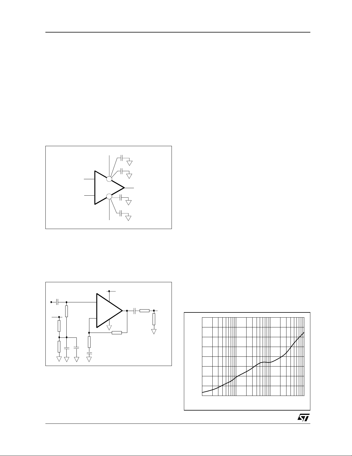
Figure 57 : Schematic Diagram
J105
J105
J106
J106
J107
J107
J108
J108
J109
J109
Differential Amplifier
Differential Amplifier
J106
J106
J109
J109
R106
R106
4
R107
R107
R102 R1 01
R102 R1 01
R103
R103
R108
R108
R109
R109
R104
R104
R110
R110
R105
R105
R107
R107
R102
R102
R110
R110
R105
R105
4
+
+
1/2TS615
1/2TS615
_
_
2
2
5
5
R114
R114
R111
R111
R112
R112
R115
R115
10
10
_
_
1/2TS615
1/2TS615
13
13
+
+
11
11
R113
R113
4
4
+
+
1/2TS615
1/2TS615
_
_
2
2
5
5
R114
R114
R111
R111
R112
R112
R115
R115
10
10
_
_
1/2TS615
1/2TS615
13
13
+
+
11
11
R113
R113
TS615
Non-Inverting Amplifier
Non-Inverting Amplifier
4
R107
J106
J106
R118
R118
R116
R116
R119
R119
R117
R117
R118
R118
R116
R116
R119
R119
R117
R117
J110
J110
R120
R120
Inverting Amplifier
Inverting Amplifier
J111
J111
R121
R121
J110
J110
R120
R120
J111
J111
R121
R121
J108
J108
Non-In ve r tin g S um m ing Amplif i er
Non-In ve r tin g S um m ing Amplif i er
J105
J105
J106
J106
R107
R102
R102
R109
R109
R104
R104
R101
R101
R106
R106
R107
R107
R102
R102
4
+
+
1/2TS615
1/2TS615
_
_
2
2
5
5
R114
R114
R111
R111
R115
R115
_
_
10
10
1/2TS615
1/2TS615
13
13
+
+
11
11
R113
R113
4
4
+
+
1/2TS615
1/2TS615
_
_
2
2
5
5
R114
R114
R111
R111
R118
R118
R116
R116
R119
R119
R117
R117
R118
R118
R116
R116
J110
J110
R120
R120
J111
J111
R121
R121
J110
J110
R120
R120
PowerSupply
PowerSupply
C102
C102
100nF
100nF
J101
J101
+Vcc
+Vcc
J102
J102
GND
GND
J103
J103
-Vcc
-Vcc
C103
C103
C103
100nF
100nF
100nF
J10412
J10412
3
3
Power down
Power down
J112
J112
+Vcc
+Vcc
C105
C105
+Vcc
+Vcc
C101
C101
100uF
100uF
C104
C104
100uF
100uF
+Vcc
+Vcc
-Vcc
-Vcc
100nF
100nF
3
3
4
4
+
+
1/2TS615
1/2TS615
_
_
5
5
C106
C106
100nF
100nF
-Vcc
-Vcc
C107
C107
100nF
100nF
100nF
100nF
+Vcc
+Vcc
_
_
10
10
1/2TS615
1/2TS615
+
+
11
11
C108
C108
R122
R122
-Vcc
-Vcc
6
6
2
2
1
1
-Vcc
-Vcc
12
12
14
14
-Vcc
-Vcc
-Vcc
-Vcc-Vcc
Expo sed-P ad
Expo sed-P ad
13
13
Differentia l Amplifier
Differentia l Amplifier
R107
J106
J106
J109
J109
R107
R102
R102
R110
R110
R105
R105
4
4
+
+
1/2TS615
1/2TS615
_
_
2
2
5
5
R114
R114
R111
R111
R112
R112
R115
R115
10
10
_
_
1/2TS615
1/2TS615
13
13
+
+
11
11
R113
R113
R118
R118
R116
R116
R119
R119
R117
R117
J110
J110
R120
R120
J111
J111
R121
R121
19/27

TS615
Figure 58 : Component Locations - Top Side
Figure 59 : Component Locations - Bottom Side
Figure 60 : Top Side Board Layout
Figure 61 : Bottom Side Board Layout
20/27

TS615
g
)
)
NOISE MEASUREMENT
Figure 62 : Noise Model
+
eN
eN
+
TS615
TS615
_
_
R2
R2
iN+
iN+
R3
R3
N3
N3
iN-
iN-
N2
N2
R1
R1
N1
N1
output
output
HP3577
HP3577
Input noi s e:
Input noi s e:
8nV/√Hz
8nV/√Hz
eN : input voltage noise of the amplifier
iNn : negative input current noise of the amplifier
iNp : positive input current noise of the amplifier
The closed loop gain is :
R
A
g1
V
The six noise sources are :
2
=
V
iNn R2×
54
V
=
V1eN
=
V3iNp R
4
V
61
V
×
2
R
------ -
–=
1
R
R
------ -
+
R
fb
--------- -+==
R
2=
kTR
2
R
------ -
1
+
1
R
2
R
31
×
2
1
-------
+
××
1
R
4
1
kTR
4
3=
kTR
Assuming the thermal noise of a resistance R as:
4kTR F∆
with
∆F the specified bandwidth.
On 1Hz bandwidth the thermal noise is reduced to
4kTR
k is the Boltzmann’s constant equals to
1,374.10-23J/°K. T is the temperature (°K).
The output noise eNo is c alculated using the Su-
perposition Theorem. But it is not the sum of all
noise sources. The output noise is the square root
of the sum of the square of each noise source.
No V12V22V32V42V52V6
+++++ eq1
2
,=
(
2
2
=
eNo2eN2g2iNn2R
2
2
R
------ -
+
4
× eq2(
1
R
+
kTR
×
21
× R
++
14
kTR
2
+
iNp
2
R
-------
+
1
R
3
× g2×
2
4
kTR
×
2
3
,
The input noise of the instrumentation must be extracted from the measured noise value. Th e real
output noise value of the driver is:
eNo Measured
()
2
instrumentation
– eq3
()
2
,=
()
The input noise is called the Equivalent Input
Noise as it is not directly measured but it is evaluated from the meas urement of the output divided
by the closed loop gain (eNo/g).
After simplification of the fourth and the fifth term
of (eq2) we obtain:
2
2
=
eNo2eN2g2iNn2R
+
… g4kTR
× eq4(),
+
× R
21
×
2
R
------ -
+
+
1
R
2
+
iNp
2
4
kTR
×
3
× g2×
3
2
Measurement of eN:
We assume a short-circuit on the non-inverting input (R3=0). (eq4) comes:
=
eNo eN2g2iNn2R
+
× eq5(),
×
2
+
g4kTR
2
×
2
In order to easily extract the value of eN, the resistance R2 will be chosen as low as possible. In the
other hand, the gain must be large enough.
R1=10Ω, R2=910Ω, R3=0, Gai n=92
Equivalent Input Noise: 2.57nV/√Hz
Input Voltage Noise: eN=2.5nV/√Hz
Measurement of iNn:
R3=0 and the output noise equation is still the
(eq5). This time the gain must be decreased to decrease the thermal noise contribution.
R1=100Ω, R2=910Ω, R3=0, Gain=10.1
Equivalent Input Noise: 3.40nV/√Hz
Negative Input Current Noise: iNn =21pA/√Hz
Measurement of iNp:
To extract iNp from (eq3), a resist ance R3 is connected to the non-inverting input. The val ue of R3
must be chose n in o rder to keep i ts therm al noise
contribution as low as possible against the iNp
contribution.
R1=100Ω, R2=910Ω, R3=100Ω, Gain=10.1
Equivalent Input Noise: 3.93nV/√Hz
Positive Input Current Noise: iNp=15pA/√Hz
Condit i ons: frequenc y=100kHz, V
Instrumentation: Spectrum Analyzer HP3585A
(input noi se of the HP358 5A: 8nV/√Hz)
CC
=±2.5V
21/27
TS615
+
-VCC
+VCC
10µF
+
10nF
TS615
10µF
+
10nF
-
+
-VCC
+VCC
10µF
+
10nF
TS615
10µF
+
10nF
-
POWER SUPPLY BYPASSIN G
A proper power suppl y bypass ing com es very im portant for optimizing the pe rformanc e in high frequency range. Bypass capacitors should be
placed as close as possible to the IC pins to improve high frequency bypassing. A capacitor
greater than 1µF is necessary to minimize the distortion. For a better quality bypassing a capacitor
of 10nF is added following the same condition of
implementation. These bypass capacitors must be
incorporated for the negative and the positive supply.
Figure 63 : Circuit for Power Supply Bypassing
SINGLE POWER SUPPLY
The following figure show the case of a 5V single
power suppl y configuration
Figure 64 : Circuit for +5V single supply
+5V
+5V
10µF
10µF
+
IN
IN
+5V
+5V
R1
R1
820Ω
820Ω
R2
R2
820Ω
820Ω
Rin
Rin
1kΩ
1kΩ
+ 1µF
+ 1µF
10nF
10nF
+
½ TS615
½ TS615
_
_
G
G
R
R
+
+
G
G
C
C
R
R
910Ω
910Ω
100µF
100µF
fb
fb
OUT
OUT
Rs
Rs
Rload
Rload
necessary to assume a positive output dynamic
range between 0V and + V
ering the values of V
OH and VOL, the am pl ifier will
supply rails. Consid-
CC
provide an output dynamic from +0.5V to 10.6V on
25Ω load for a 12V supplying, from 0.45V to 3.8V
on 10 Ω load for a 5V supplying.
The amplifier must be biased with a mid supply
(nominally +V
/2), in order to maintain the DC
CC
component of the signa l at this val ue. Several options are possible to provide this bias supply (such
as a virtual ground using an operational amplifier),
or a two-resistance di vider which is the cheapest
solution. A high resistance value is required to limit the current consumption. On the other hand, the
current must be high enough to bias the non-inverting input of t he amplifier. If we consider this
bias current (30µA max.) as the 1% o f the current
through the resistance divider to keep a stable mid
supply, two resistances of 2.2kΩ can be used i n
the case of a 12V power supply and two resistances of 820Ω can be used in the case of a 5V power
supply.
The input provides a hig h pass filter with a break
frequency below 10Hz which is necessary to remove the original 0 volt DC component of the input
signal, and to fix it at +V
CC
/2.
CHANNEL SEPARATION - CROSSTALK
The following figure show the crosstalk from an
amplifier to a second amplifier. This phenomenon,
accented in high frequ encies, is unavoidable and
intrinsic of the circuit.
Nevertheless, the PCB layout has also an effect
on the crosstalk level. Capacitive coupling between signal wires, distance between critical signal nodes, power supply bypassing, are the most
significant points.
Figure 65 : Crosstalk vs. Frequency
AV=+4, Rfb=620Ω, VCC=±6V, Vout=2Vp
-50
-60
-70
-80
-90
The TS615 operates from 12V down to 5V power
supplies. This is achieved with a d ual power s up-
ply of ±6V an d ±2.5V or a s ingle power s upply of
12V and 5V referenced to the grou nd. In t he cas e
of this asymmet rical supp lying, a new biasing is
22/27
-100
CrossTalk (dB)
-110
-120
-130
10k 100k 1M 10M
Frequency (Hz)

TS615
0 1020304050
-6
-5
-4
-3
-2
-1
0
Vout
Vpdw
Disabled Output
Enabled Output
(Volts)
Time (µs)
POWER DOWN MODE BEHAVIOUR
Figure 66 : Equivalent Schematic
V
cc +
3
.
+
Vcc -
V
+
V
.
A1
_
cc -
A2
_
cc
+
..
.
pdw
R
1
14
.
.
12
-Vcc
-Vcc
Rpdw
.
..
13
4
5
11
10
2
Ouput 1
Ouput 2
POWER
DOWN
pin6
POWER
DOWN
pin6
Please note that the short circuited output in power down mode is referenced to (-
V
). No problem
CC
appears when used in differential mode. Nevertheless, when used in single ended on a load referenced to GND, the (-
V
) level contributes to a
CC
current consumption through the load. As described on t he Figure 68, t he interest of featuring
an output short circuit in power down mode is to
keep the best impedance matchi ng between the
system and the twisted pair telephone line when
the modem is in sleep mode. By this way, the modem can be waked-up with a sign al from the line
without any damage of this signal. This concept is
particularly intended for the ADSL over voice modems, where the modem in sleep mode, must be
waked-up by the phone call.
Figure 67 : Matching in Sleep Mode
Figure 68 : Standby Mode. Time On>Off
Figure 69 : Standby Mode. Time Off>On
1
0
Disabled Output
−1
−2
(Volts)
−3
−4
−5
−6
012345
Time (µs)
Enabled Output
Vout
Vpdw
Figure 70 : Standby Mode. Input/Output Isolation
vs. Frequency
AV=+4, Rfb=620Ω, VCC=±6V, Vout=3Vp
Consumption=80µA
Consumption=80µA
12.5Ω
12.5Ω
TS615
TS615
POWER DOWN
POWER DOWN
5Ω max.
5Ω max.
12.5Ω
12.5Ω
The system can be waked-up
The system can be waked-up
from the line
from the line
Matching
Matching
25Ω
25Ω
Transformer
Transformer
1:2
1:2
Line (100Ω)
Line (100Ω)
0
-10
-20
-30
-40
-50
-60
-70
-80
Isolation (dB)
-90
-100
-110
-120
-130
10k 100k 1M 10M
Frequency (Hz)
23/27
TS615
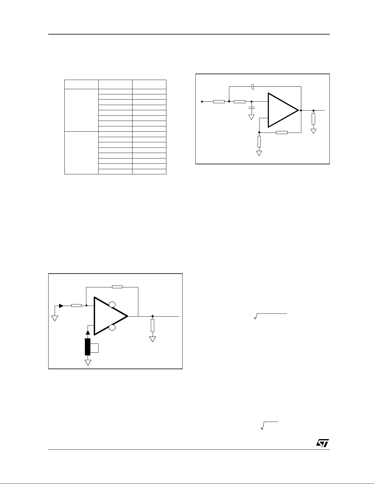
CHOICE OF THE FEEDBACK CIRCUIT
Table 71 : Closed-Loop Gain - Feedback Compo-
nents
V
CC
±6
±2.5
(V)
Gain
+1 750
+2 680
+4 620
+8 510
-1 680
-2 680
-4 620
-8 510
+1 1.1k
+2 1k
+4 910
+8 680
-1 1k
-2 1k
-4 910
-8 680
Rfb (Ω)
INVERTING AMPLIFIER BIASING
In this case a resistance is necessary to achieve a
good input biasing, as R on (fig.30).
This resistance is calculated by assuming the negative and positive input bias current. The aim is to
make the compensation of the offset bias current
which could affect the input offset voltage and t he
output DC component . A ssumin g I b-, Ib+ , R
in, Rfb
and a zero volt output, the resistance R comes: R
= R
in // Rfb .
Figure 72 : Compensation of the Input Bias
Current
ACTIVE FI LT ER I N G
Figure 73 : Low-Pass Active Filtering. Sallen-Key
C1
C1
1 R2
1 R2
R
R
IN
IN
The resistors R
fb and RG give d irectly the gain of
+
+
C2
C2
RG
RG
_
_
TS615
TS615
910Ω
910Ω
R
R
fb
fb
OUT
OUT
25Ω
25Ω
the filter as a classical non-inverting amplification
configuration :
R
A
V
g1
fb
--------- -+==
R
g
Assuming the following expression as the response of the system:
Vout
T
j
ω
------------------Vin
j
ω
j
ω
---------------------------------------------==
12
------ -
ζ
ω
j
ω
g
c
j
ω()
--------------++
2
ω
c
2
Ib-
Ib-
24/27
Rin
Rin
Ib+
Ib+
R
R
fb
fb
the cutoff frequency is not gain depe ndent and it
Vcc+
TS615
TS615
Vcc+
Vcc-
Vcc-
Output
Output
Load
Load
_
_
+
+
R
R
comes:
------------------------------------- -=
ω
c
R1R2C1C2
the damping factor comes:
1
-- -
=
ζ
ω
()
cC1R1C1R2C2R1C1R1
2
1
g–++
The higher the gain the more sensitive the damping factor is. When the gain is hig her than 1 it is
preferable to use som e very stable resistors and
capacitors values.
In the case of R1=R2:
R
2C2C
------------------------------------=
ζ
2C1C
fb
--------- -–
1
R
g
2
TS615
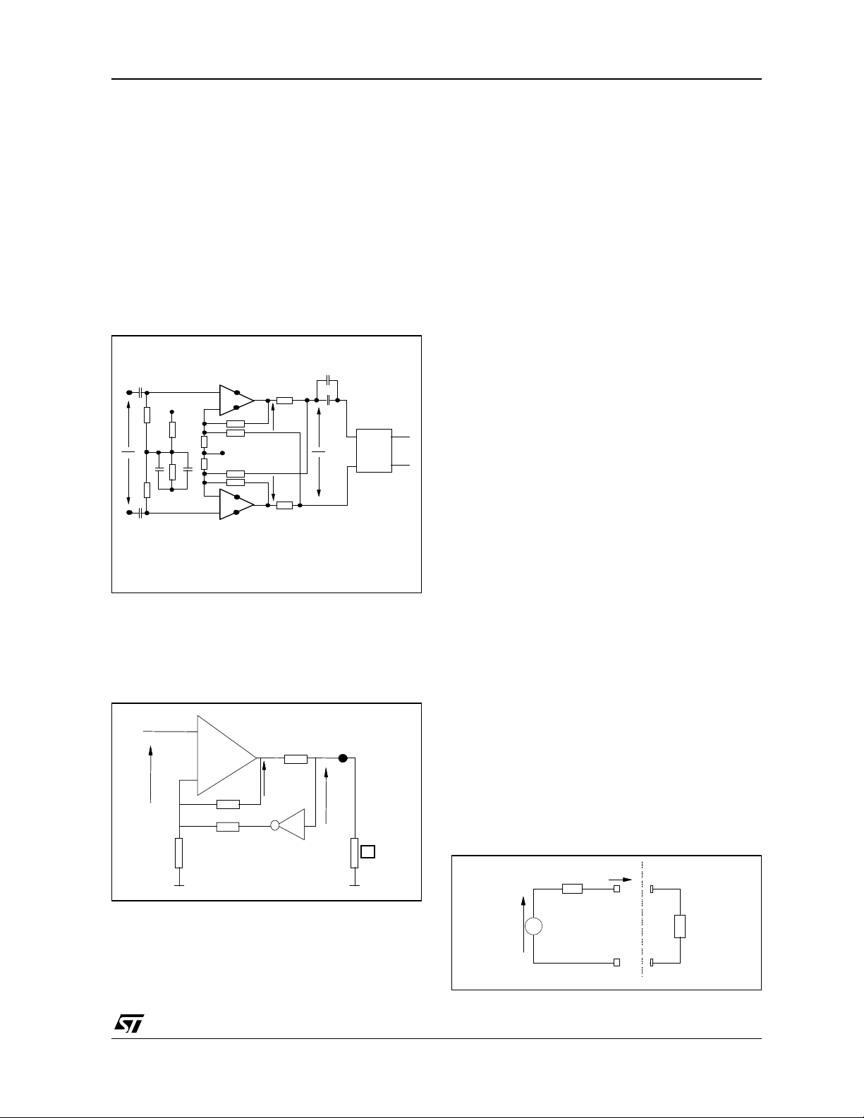
INCREASING THE LINE LEVEL BY USING AN
ACTIVE IMPEDANCE MATCHING
With a passive mat ching, the output signal amplitude of the driver must be twice the amplitude on
the load. To go beyond this limitation an active
matching impedance can be used. With this technique, it is possible to keep a good impedance
matching with an amplitude on the load higher
than the half of the output driver amplitude. This
concept is shown in figure 74 for a differential line.
Figure 74 : T S615 as a differential line driver with
an active impedance matching
µ
100n
Vcc+
1k
Vi
100n
100n
10µ
1k
GND
Vi Vo
1/2 R1
1/2 R1
+
_
+
_
R2
R3
Vcc/2
R5
Vcc+
Rs1
GND
Vo°
Vcc+
GND
Vo°
Rs2
R4
1
10n
Vo
1:n
Hybrid
&
RL
Transformer
100Ω
2Vi
Vi Vo°–
()
---------
---------------------------and
R1
As Vo
° equals Vo without load, the gain in this
R2
Vi Vo+
()
------------------------,
R3
case becomes :
2R2
----------R1
R2
1
–
------- R3
R2
------- -++
R3
G
Vo noload
()
--------------------------------Vi
1
------------------------------------==
The gain, for the loaded system will be (eq1):
2R2
----------R1
R2
1
------- -–
R3
R2
------- -++
R3
,==
()
GL
Vo withload
()
-------------------------------------Vi
1
1
-- -
------------------------------------ e q1
2
As shown in figure76, this system is an ideal generator with a synthesized impedance as the internal impedance of the system. From this, the output voltage becomes:
Vo ViG
()
RoIout
–= eq2
()
,
()
with Ro the synthesized impedance and Iout the
output current. On the other hand Vo can be expressed as:
Component Calculation
Let us consider the equivalent c ircuit for a single
ended configuration, Figure75.
Figure 75 : Single ended equivalent circuit
+
1/2
1/2
+
Vi
Vi
R1
R1
R2
R2
_
_
R3
R3
Vo°
Vo°
Rs1
Rs1
-1
-1
Vo
Vo
1/2
1/2
RL
RL
Let us consider the unloaded system . Assumi ng
the currents through R1, R2 and R3
as respectively:
2R2
----------R1
R2
------- -–
R3
R2
------- -++
R3
Rs1Iout
----------------------- eq 3
1
R2
------- -–
R3
,–=
()
Vi 1
Vo
------------------------------------------------
1
By identification of both equations (eq2) and
(eq3), the synthesized impedance is, with
Rs1=Rs2=Rs:
Ro
Rs
----------------- e q 4
,=
()
R2
1
------- -–
R3
Figure 76 : Equivalent schematic. Ro is the
synthesized impedance
Ro
Vi.Gi
Iout
1/2RL
25/27
TS615
Unlike the level Vo° required for a passive impedance, Vo
us write Vo
° will be smaller than 2Vo in our case. Let
°=kVo with k the m at ching f actor vary -
ing between 1 and 2. Assum ing that the current
through R3 is negligible, it comes the following resistance divider:
Ro
kVoRL
----------------------------- -=
RL 2Rs1+
After choosing the k factor, Rs will equal to
1/2RL(k-1).
A good impedance matching assume s:
1
Ro
-- -RL eq5
,=
()
2
From (eq4) and (eq5) it becomes:
R2
------- -1
R3
2Rs
----------- eq 6
,–=
()
RL
By fixing an arbitrary value of R2, (eq6) gives:
R3
R2
-------------------- -=
2Rs
1
-----------–
RL
Finally, the values of R2 and R3 allow us to extract
R1 from (eq1), and it comes:
----------------------------------------------------------- eq 7
R1
21
2R2
R2
–
GL 1–
------- -
R3
R2
–
------- R3
,=
()
with GL the required gain.
Figure 77 : Components Calculation for
Impedance Matching Implem entat ion
GL (gain for the
loaded system)
R1 2R2/[2(1-R2/R3)GL-1-R2/R3]
R2 (=R4) Abritra ry fixed
R3 (=R5) R2/(1-Rs/0.5RL)
Rs 0.5RL(k-1)
Load view ed by
each driv er
GL is fixed for the application requirements
GL=Vo/Vi=0.5(1+2R2/R1+R2/R3)/(1-R2/R3)
kRL/2
26/27

PACKAGE MECHANICAL DATA
14 PINS - THIN SHRINK SMALL OUT L INE PACKAGE (TSSOP Exposed-Pad)
c
k
0,25 mm
GAUGE PLANE
L
L1
C
PLANE
SEATING
E
E2
89
e
E1
A
A2
A1
TS615
D1
1
PIN 1 IDENTIFICATION
14
D
b
C
aaa
Millimeters Inches
Dimensions
Min. Typ. Max. Min. Typ. Max.
A 1.200 0.047
A1 0.150 0.006
A2 0.800 1.000 1.050 0.031 0.039 0.041
b 0.190 0.300 0.007 0.012
c 0.090 0.200 0.004 0.008
D 4.900 5.000 5.100 0.193 0.197 0.201
D1 3.000 1.18
E 6.200 6.400 6.600 0.244 0.252 0.260
E1 4.300 4.400 4.500 0.169 0.173 0.177
E2 3.000 1.18
e 0.650 0.026
L 0.450 0.600 0.750 0.018 0.024 0.030
L1 1.000 0.039
k0d 8d0d 8d
aaa 0.100 0.004
Information furnished is bel ieved to be accurate and reliable. However, STMicroe lectronics assumes no responsibility for the
consequences of use of such information nor for any infringement of patents or other rights of third parties which may result from
its use. No li cense is granted by imp lication or otherwise under a ny patent or patent rig hts of STMicroelectronics. Spec ific at ions
mentioned in this publication ar e subject to change without notice. This publication supersedes and replaces all information
previously supplied. S TMicroelectronics products are not authorized for use as critica l components in life suppo rt devices or
systems without express written approval of STMicroelectronics.
© The ST logo is a registered trademark of STMicroelectronics
© 2002 STM icroelectronics - Printed in Ital y - All Rights Reserved
STMicr o el ectronics GROUP OF COMPA NI E S
Australi a - Brazil - Chi na - Finland - F rance - Germany - Hong Kon g - I ndia - Italy - Japan - Malay sia - Malta - Morocco
Singapo re - Spain - Sweden - Switzerland - Uni ted Kingdom
© http://www.st.com
27/27
 Loading...