

SGS Thomson Microelectronics TS514AIN, TS514AID, TS514 Datasheet
QUAD OPERATIONAL AMPLIFIERS
.
LOW OFFSETVOLTAGE: 500µVmax.
.
LOW POWERCONSUMPTION
.
SHORT CIRCUIT PROTECTION
.
LOW DISTORTION, LOW NOISE
.
HIGHGAIN-BANDWIDTHPRODUCT
.
HIGHCHANNEL SEPARATION
.
ESD INTERNALPROTECTION
.
MACROMODEL INCLUDED IN THIS
SPECIFICATION
DESCRIPTION
The TS514is ahighperformancequadoperational
amplifier with frequencyand phase compensation
builtintothechip.Theinternalphasecompensation
allows stable operationas voltagefollowerin spite
of its high gain-bandwidthproducts.
The circuit presents very stable electrical characteristics over the entire supply voltage range, and
it particularlyintendedfor professionalandtelecom
applications(active filters, etc).
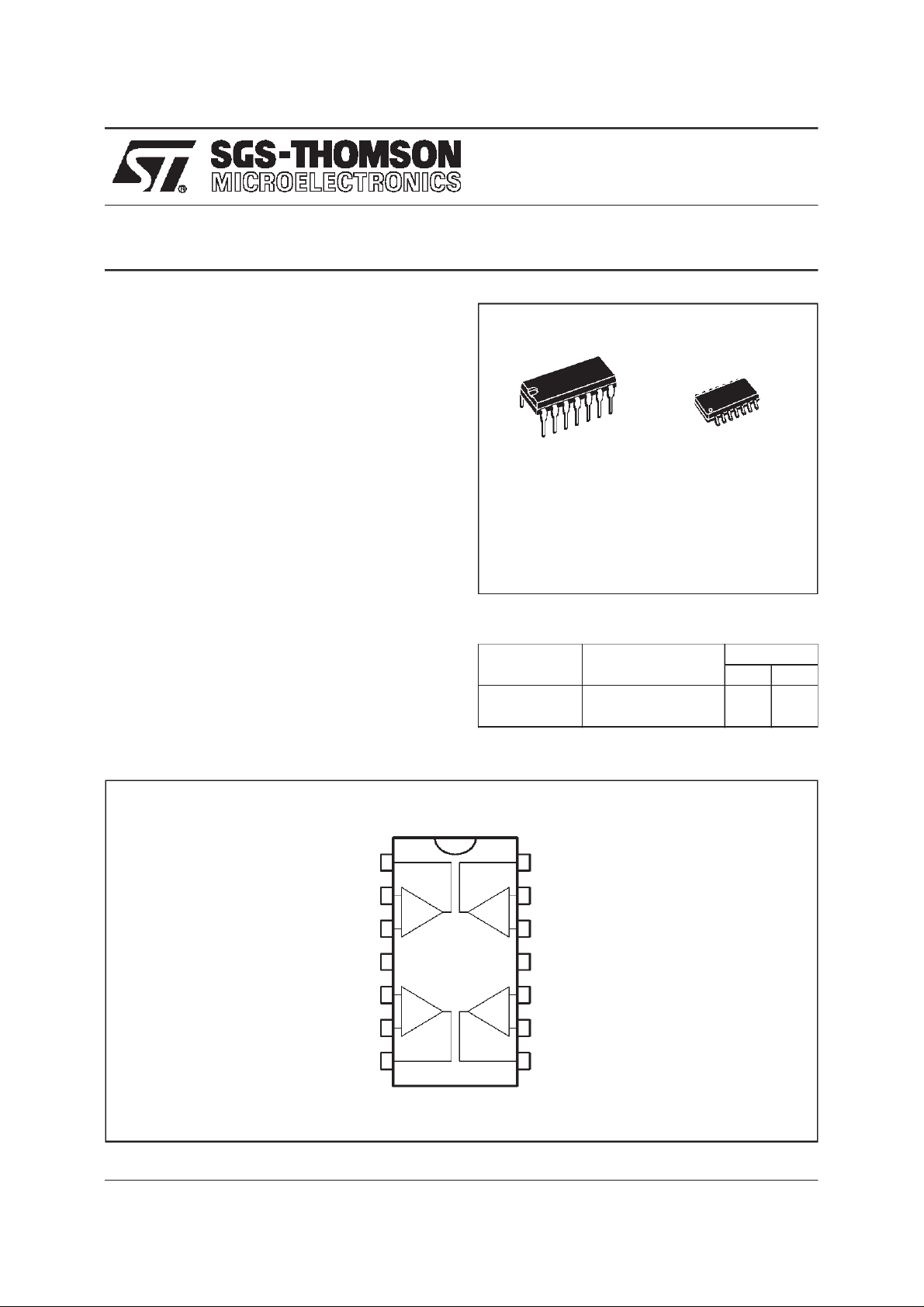
TS514,A
HIGH SPEED PRECISION
N
DIP14
(Plastic Package)
ORDER CODES
Part Number Temperature Range
TS514I -40
TS514AI -40
(Plastic Micropackage)
o
C, +125oC ••
o
C, +125oC ••
D
SO14
Package
ND
PINCONNECTIONS (top view)
Output 1
Inverting Input 1
Non-inverting Input 1
Non-inverting Input 2
Inverting Input 2
Output2
December 1997
1
2
-
+
3
+
CC
4
5
+
-
6
7
V
14
Output 4
Inverting Input 4
13
-
+
+
-
Non-inverting Input 4
12
-
V
11
CC
Non-inverting Input 3
10
Inverting Input 3
9
8
Output 3
1/7
TS514,A
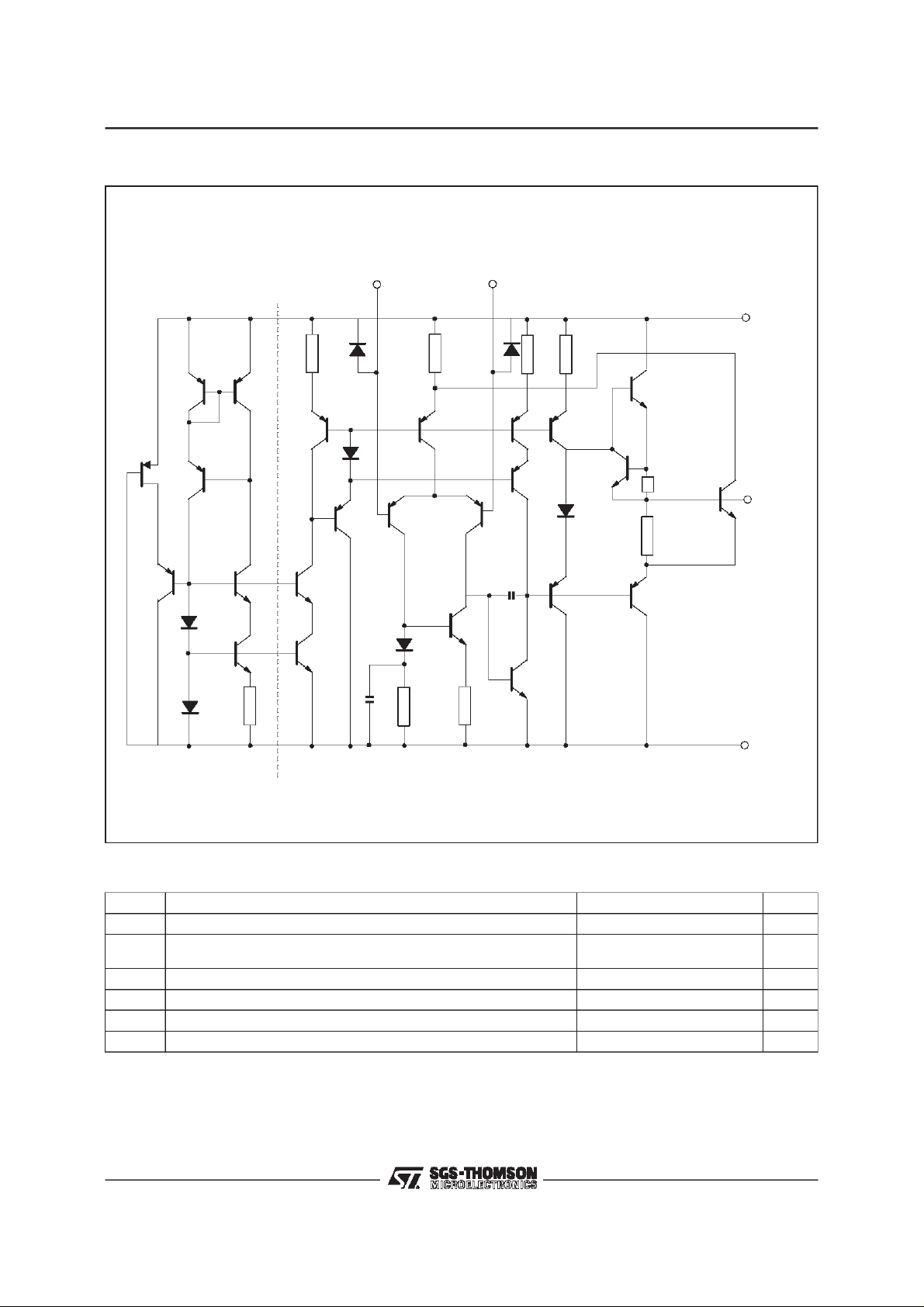
SCHEMATIC DIAGRAM (1/2 TS514)
Q17
R5
D3
D4
Q1
Q7
Q2
Q18
Q21
R8
Q3
Q19
Q22
R1
D6
Inverting
input
D1
Q8
D5
C2
Q10
R9
Non-inverting
R2
Q4
Q11
Q23
R10
input
D7
C1
Q9
Q20
Q5
R3
Q6
Q15
R4
D2
Q12
8
Q13
Q14
R6
Output
R7
Q16
4
ABSOLUTEMAXIMUM RATINGS
Symbol Parameter Value Unit
V
V
T
P
T
2/7
Supply Voltage ±18 V
CC
Input Voltage (positive)
V
i
Differential Input Voltage ± (VCC-1)
id
Operating Temperature Range -40 to +125
oper
Power Dissipation at T
tot
Storage Temperature -65to 150
stg
(negative)
=70oC 400 mW
amb
+V
CC
-VCC- 0.5
V
o
C
o
C

TS514,A
ELECTRICALCHARACTERISTICS (VCC= ±15V,T
= 25oC, unless otherwise specified)
amb
Symbol Parameter Test Conditions Min. Typ. Max. Unit
I
R
V
DV
I
DI
I
A
Supply Current 1.4 2.4 mA
CC
Input Bias Current 50 150 nA
I
ib
T
min.<Top<Tmax
Input Resistance f = 1kHz 1 MΩ
i
Input Offset Voltage TS514
io
T
min.<Top<Tmax
Input Offset Voltage Drift T
io
Input Offset Current 5 20 nA
io
Input Offset Current Drift T
io
Output Short Circuit Current 23 mA
os
Large SignalVoltage Gain RL=2kΩ VCC= ±15V
vd
.<Top<T
min
.<Top<T
T
min
.<Top<T
min
. 300 nA
0.5 2.5
TS514A
. TS514
TS514A
.5µV/oC
max
.40nA
max
. 0.08 nA
max
90 100
= ±4V
V
CC
95
0.5
4
1.5
GBP Gain-bandwidth Product f = 100kHz 1.8 3 MHz
e
THD Total Harmonic Distortion A
±V
V
Equivalent Input Noise Voltage f = 1kHz
n
Output Voltage Swing RL=2kΩ VCC= ±15V
opp
Large SignalVoltage Swing RL= 10kΩ f = 10kHz 28 V
opp
=50Ω
R
s
=1kΩ
R
s
= 10kΩ
R
s
= 20dB RL=2kΩ
V
=2VPPf = 1kHz
V
O
V
CC
= ±4V
8
10
18
0.03 0.1 %
±13
±3
15
√Hz
SR Slew Rate Unity Gain, RL=2kΩ 0.8 1.5 V/µs
CMR Common Mode Rejection Ratio V
SVR Supply Voltage Rejection Ratio V
V
O1/VO2
Channel Separation f = 1kHz 100 120 dB
= 10V 90 dB
ic
= 1V f = 100Hz 90 dB
ic
mV
mV
°C
dB
nV
V
PP
3/7
 Loading...