

TS507
High Precision Rail-to-Rail Operational Amplifier
PRELIMINARY DAT A
■ Ultra low offset voltage: 60µV max
■ Rail-to rail input/output voltage swing
■ Operating from 2.7V to 5.5V
■ High-speed: 2.2MHz
■ Low consumption: 0.85mA
■ Supply voltage rejection ratio: 85d B
■ ESD protection 2kV
■ Latch-up immunity
■ Available in SOT23-5 micropackage
Description
The TS507 is a high performance rail-to-rail
output amplifier with very lo w offset voltage. This
amplifier uses a new trimming technique that
yields ultra low offset voltages without any need
for exter na l nu llin g.
The circuit presents very stable electrical
characteristics over the entire supply voltage
range, and is particularly intended for professional
and telecom applications.
The TS507 is housed in the spac e-saving 5 pins
SOT23 package that makes it well suited for
battery-powered systems. This micropackage
simplifies the PC board design because of it’s
ability to be placed in tight spaces (outside
dimensions are: 2.8mm x 2.9mm)
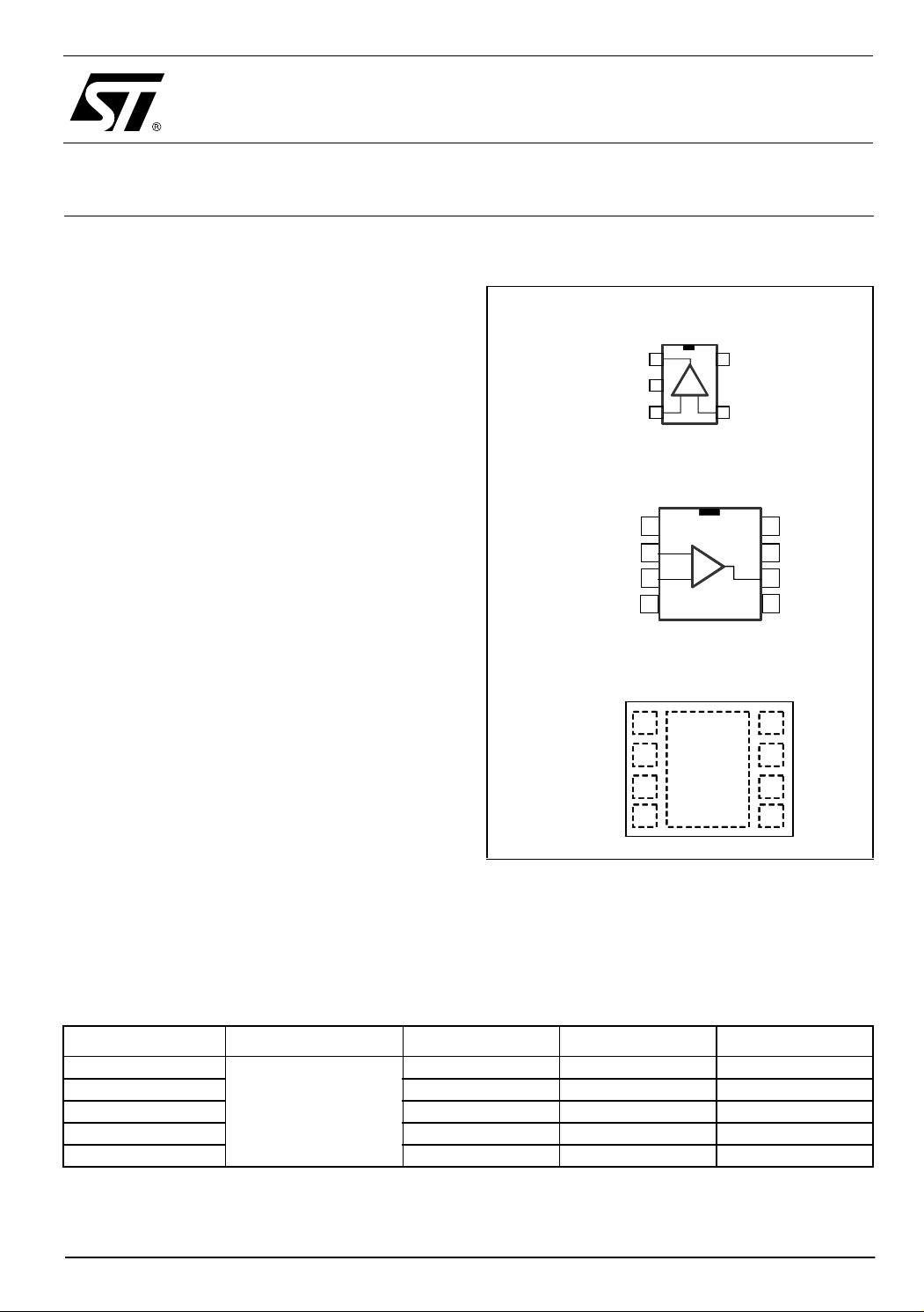
Pin Connections (top view)
TS507ILT
Output
Output
1
1
VDD
VDD
2
2
Non Inverting Input Inverting Input
Non Inverting Input Inverting Input
TS507ID-TS507IN-TS507IST
Inverting Input
Inverting Input
Non Inverting Input
Non Inverting Input
Inverting Input
Inverting Input
Non Inverting Input
Non Inverting Input
VDD
VDD
3
3
N.C.
N.C.
1
1
_
_
2
2
+
+
3
3
VDD
VDD
4
4
TS507IQT
NC
NC
1
1
2
2
3
3
45
45
VCC
VCC
5
5
4
4
8
N.C.
8
N.C.
VCC
VCC
7
7
Output
Output
6
6
N.C.
N.C.
5
5
NC
NC
8
8
VCC
VCC
7
7
Output
Output
6
6
NC
NC
Applications
■ Precision filters
■ Transformer/line driver s
■ Personal entertainments (CD players)
■ Portable communication (cell phones,
pagers)
■ Instrumentation & sensoring
Order Codes
Part Number Temperature Range Package Packaging Marking
TS507IN
TS507ID/TS507IDT DIP Tube or Tape & Reel
TS507IST mini SO Tape & Reel
-40, +125°C
TS507ILT SOT23-5 Tape & Reel TBD
TS507IQT DFN Tape & Reel
November 2004 Revision 1 1/9
This is preliminary information on a new product now in development or undergoing evaluation. Details are subject to change without noti c e .
DIP Tube
TS507 Absolute Maximum Ratings
1 Absolute Maximum Rat ings
Table 1: Key parameter s and their abs olute maxi mum ratin gs
Symbol Parameter Value Unit
VCC
Vid
V
in
T
oper
Supply voltage
Differential Input Voltage
Input Voltage
Operating Free Air Temperature Range
1
2
3
Tstg Storage Temperature Range -65 to +150
T
Maximum Junction Temperature
j
Thermal Resistance Junction to Case
4
SOT23-5
Rthjc
SO8
DIP8
Rthja Thermal Resistance Junction to Ambient - SOT23-5 256 °C/W
ESD Human Body Model 2 kV
Lead Temperature (soldering, 10sec ) 260 °C
1) All voltage values, except dif fe rential volt age are wit h respect to net work ground termina l .
2) Differential voltages are the non-inver ting input termi nal with re spect to the inverting i nput t erminal .
3) The magni tude of input and output vol tages must never exceed VCC +0.3V.
4) Short-circuits can cause excessive heating and destructive dissipation.
6V
±5.5 V
Gnd to Vcc V
-40 to +125 °C
150 °C
°C/W
81
28
80
Table 2:
Operating Conditions
Symbol Parameter Value Unit
V
V
Supply voltage
CC
Common Mode Input Voltage Range
icm
2.7 to 5.5 V
-0.2 to VCC +0.1
V
DD
V
2/9
Electrical Characteristics TS507
2 Electrical Characteristics
Table 3: V
+
= +5V, V
CC
Symbol Parameter Min. Typ. Max. Unit
I
Supply Current 0.85 mA
cc
Input Bias Current
I
ib
Input Resistance, f = 1kHz 1 MΩ
R
i
T
min
≤ Top ≤ T
Input Offset Voltage
V
io
∆V
Input Offset Voltage Drift
io
I
io
∆I
io
I
os
A
vd
T
≤ Top ≤ T
min
Input Offset Current
T
≤ Top ≤ T
min
Input Offset Current Drift
T
≤ Top ≤ T
min
Output Short Circuit Current 50 mA
Large Signal Voltage Gain
R
= 2kΩ 1V ≤ V
L
GBP Gain-bandwidth Product, f = 100kHz 2.2 MHz
Equivalent Input Noise Voltage, f = 1kHz
e
n
Rs = 1k
Total Harmonic Distortion
= 20dB RL = 2kΩ
THD
A
v
Vo = 2V
±V
V
Output Voltage Swing
opp
opp
SR
R
= 2kΩ TBD
L
Large Signal Voltage Swing
= 10kΩ f = 10kHz TBD
R
L
Slew Rate
Unity Gain, RL = 2kΩ 0.65
PSRR Power Supply Rejection Ratio 100 dB
Common Mode Rejection Ratio
V
CMRR
= 0V to 3.5V
ic
= 0V to 5V
V
ic
-
DD
= 0V, T
= 25°C (unless otherwise specified) - Operational Amplifier
amb
50
max
0V
T
min
≤ V
≤ T
≤ 3.5V
CM
op
≤ T
max
TBD
0V ≤ VCM ≤ 5V
≤ T
≤ T
max
0.3
0.08
≤ 4V 125
max
max
max
T
min
op
out
Ω 12
TDB
pp
f = 1kHz
125
94
150 nA
060
100
300
350
µV/°C
5TBD
TBD
µV
nA
nA
------°C
dB
nV
----------- Hz
%
V
V
pp
µs
V/
dB
3/9

TS507 Package Mechanical Data
3 Package Mechanical Data
3.1 DIP-8 Package
Plastic DIP-8 MECHANICAL DATA
DIM.
A 3.3 0.130
a1 0.7 0.028
B 1.39 1.65 0.055 0.065
B1 0.91 1.04 0.036 0.041
b 0.5 0.020
b1 0.38 0.5 0.015 0.020
D 9.8 0.386
E 8.8 0.346
e 2.54 0.100
e3 7.62 0.300
e4 7.62 0.300
F 7.1 0.280
I 4.8 0.189
L 3.3 0.130
Z 0.44 1.6 0.017 0.063
MIN. TYP MAX. MIN. TYP. MAX.
mm. inch
4/9
P001F

Package Mechanical Data TS507
3.2 SO-8 Package
SO-8 MECHANICAL DATA
DIM.
A 1.35 1.75 0.053 0.069
A1 0.10 0.25 0.04 0.010
A2 1.10 1.65 0.043 0.065
B 0.33 0.51 0.013 0.020
C 0.19 0.25 0.007 0.010
D 4.80 5.00 0.189 0.197
E 3.80 4.00 0.150 0.157
e 1.27 0.050
H 5.80 6.20 0.228 0.244
h 0.25 0.50 0.010 0.020
L 0.40 1.27 0.016 0.050
k ˚ (max.)
ddd 0.1 0.04
MIN. TYP MAX. MIN. TYP. MAX.
mm. inch
8
5/9

TS507 Package Mechanical Data
3.3 Mini SO-8 Package
6/9

Package Mechanical Data TS507
3.4 SOT23-5 Package
SOT23-5L MECHANICAL DATA
DIM.
MIN. TYP MAX. MIN. TYP. MAX.
A 0.90 1.45 35.4 57.1
A1 0.00 0.15 0.0 5.9
A2 0.90 1.30 35.4 51.2
b 0.35 0.50 13.7 19.7
C 0.09 0.20 3.5 7.8
D 2.80 3.00 110.2 118.1
E 2.60 3.00 102.3 118.1
E1 1.50 1.75 59.0 68.8
e.95 37.4
e1 1.9 74.8
L 0.35 0.55 13.7 21.6
mm. mils
0
7/9

TS507 Package Mechanical Data
3.5 DFN8 Package
8/9

Revision History TS507
4 Revision History
Date Revision Description of Changes
01 Oct 2004 1 First Release
Information furnished is believed to be accurate and reliable. However, STMicroelectronics assumes no responsibility for the consequences
of use of such information nor for any infringement of patents or other rights of third parties which may result from its use. No license is granted
by implic ation or oth erwise under any pat ent or pat ent rights of STMicroe l ectronics . Specificati ons menti oned in thi s publication are subject
to change without notice. This publication supersedes and replaces all information previously supplied. STMicroelectronics products are not
authoriz ed for use as critical comp onents in lif e support dev i ces or systems wi thout exp res s written ap proval of STMi croelectronics.
The ST logo i s a registered trademark of STMicroelectronics
All other nam es are the pro perty of thei r respectiv e owners
© 2004 STMi croelectro ni cs - All rights reserved
Australi a - Belgium - B razil - Canada - China - Czech Republi c - Finland - F rance - Germ any - Hong Ko ng - I ndi a - Israel - It al y - Japan -
Malaysia - M al ta - Morocco - Singapore - Spain - Swe den - Switze rl and - Unite d Kingdom - United States of Americ a
STMicroelectron ics group of com panies
www.st.com
9/9
 Loading...