

1W AUDIO POWER AMPLIFIER WITH ACTIVE LOW
■OPERATING FROM V
■1W OUTPUT POWER @ Vcc=5V, THD=1%,
f=1kHz, with 8
Ω Load
■ULTRA LOW CONSUMPTION IN STANDBY
MODE (10nA)
■62dB PSRR @ 217Hz @ Grounded mode
■Zero PO P & CLIC K
■ULTRA LOW DISTORTION (0.1%)
■UNITY GAIN STABLE
■AVAILABLE IN 9 BUMPS Flip Chip Package
= 2.2V to 5.5V
CC
STANDBY MODE
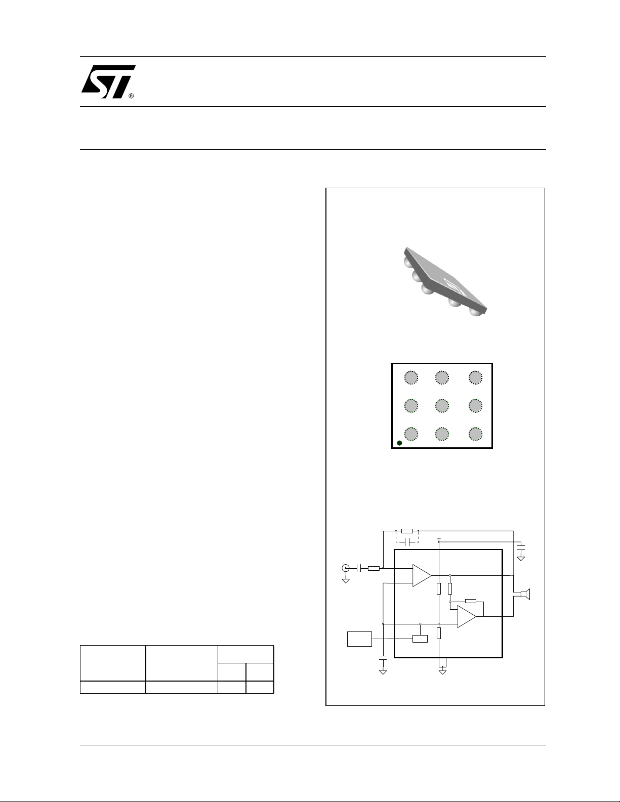
PIN CONNECTIONS (top view)
TS4990JT - FLIP CHIP
TS4990
ADVANCE DATA
DESCRIPTION
The TS4990 has been designed for demanding
audio applications such as m obile phones and t o
minimize the number of external components.
This Audio Power Amplifier is capable of delivering 1W of continuous RMS Ouput Powe r into an
Ω load @ 5V.
8
An externally controlle d standby m ode control re-
duces the supply current to less than 10nA. It also
includes an internal thermal shutdown protection.
The unity-gain stable amplifier can be configured
by external gain setting resistors.
APPLICATIONS
■Mobile Phones (Cellular / Cordless)
■Laptop / Notebook Computers
■PDAs
■Portable Audio Devices
ORDER CODE
Part Number
Temperature
Range
TS4990IJT -40, +85°C
Package
J
•
6
6
Vin-
Vin-
7
7
8
8
1
1
BYPASS VOUT2
BYPASS VOUT2
Vout1
Vout1
GNDGND VCC
GNDGND VCC
9
9
2
2
TYPICAL APPLICATION SCHEMATIC
Rfeed
Audio In
Cin
Standby
Control
Cfeed
Rin
7
Vin-
5
Vin+
1
Bypass
3
Standby
+
Cb
Vcc
48
VCCGND
-
+
-
AV = -1
+
Bias
9
Vin+
Vin+
STBY
STBY
Vout 1
Vout 2
TS4990
5
5
4
4
3
3
+
Cs
6
Speaker
8 Ohms
2
J = Flip Chip Package - only available in Tape & Reel (JT)
February 2003
This is a preliminary information on a new product now in development. Details are subject to change without notice.
1/6
TS4990
ABSOLUTE MAXIMUM RATINGS
Symbol Parameter Value Unit
V
T
T
R
Supply voltage
CC
V
Input Voltage
i
Operating Free Air Temperature Range -40 to + 85 °C
oper
Storage Temperature -65 to +150 °C
stg
T
Maximum Junction Temperature 150 °C
j
thja
Thermal Resistance Junction to Ambient
Flip Chip
Pd Power Dissipation Internally Limited
ESD Human Body Model 2 kV
ESD Machine Model 200 V
Latch-up Immunity Class A (200mA)
Lead Te mpera ture (solde ring, 10sec ) 250 °C
1. All voltages values are measured with respect to the ground pin.
2. The magnitude of input signal must never exceed V
3. Device is protected in case of over temperature by a thermal shutdown active @ 150°C.
OPERATING CONDITIONS
Symbol Parameter Value Unit
V
V
V
R
GND
T
R
Supply Voltage 2.2 to 5.5 V
CC
Common Mode Input Voltage Range
ICM
Standby Voltage Input :
STB
Device ON
Device OFF
R
Load Resistor 4 - 32
L
OUT
Resistor Output to GND > 1 M
Thermal Shutdown Temperature 150 min. °C
SD
thja
Thermal Resistance Junction to Ambient
1)
2)
3)
+ 0.3V / GND - 0.3V
CC
1.2 ≤ V
GND ≤ V
1)
6V
GND to V
CC
TBD
1.2V to V
STB
STB
CC
≤ V
≤ 0.4
CC
TBD °C/W
V
°C/W
V
V
Ω
Ω
1. This thermal resistance can be reduced with a suitable PCB layout .
2/6

TS4990
ELECTRICAL CHARACTERISTICS
V
= +5V, GND = 0V , T
CC
Symbol Parameter Min. Typ. Max. Unit
= 25°C (unless otherwise specified)
amb
I
CC
I
STANDBY
Voo
Po
THD + N
PSRR
T
WU
1. Standby mode is actived wh en Vstdby is tied to Gnd
2. Dynamic mea surements - 20*log(rms(Vout )/ rms(Vri ppl e)). Vripple is the suri mposed s i nus signal to Vc c.
= +3.3V, GND = 0V, T
V
CC
Supply Current
No input signal, no load 4 6
Standby Current
No input signal, Vstdby = GND, RL = 8
1)
Ω
10 1000 nA
Output Offset Voltage
No input signal, RL = 8
Ω
Output Power
THD = 1% Max, f = 1kHz, RL = 8
Ω
Total Harmonic Distortion + Noise
Po = 250mW rms, Gv = 2, 20Hz < f < 20kHz, RL = 8
Power Supply Rejection Ratio
RL = 8
Gv = 2, Vripple = 200mVpp, Input Grounded
Ω,
2)
F = 217Hz
F = 1kHz
0.8 1 W
Ω
55
55
520
0.15 %
62
66
Wake-Up Time 100 TBD ms
= 25°C (unless otherwise specified)
amb
Symbol Parameter Min. Typ. Max. Unit
I
CC
I
STANDBY
Supply Current
No input signal, no load 4 6
Standby Current
No input signal, Vstdby = GND, RL = 8
1)
Ω
10 1000 nA
mA
mV
dB
mA
Voo
Po
THD + N
PSRR
T
WU
1. Standby mode i s actived when Vstdby is tied to Vcc
2. Dynamic mea surements - 20*log(rms(Vout )/ rms(Vri ppl e)). Vripple is the suri mposed s i nus signal to Vc c.
Output Offset Voltage
No input signal, RL = 8
Output Power
THD = 1% Max, f = 1kHz, RL = 8
Ω
Ω
380 450 mW
Total Harmonic Distortion + Noise
Po = 250mW rms, Gv = 2, 20Hz < f < 20kHz, RL = 8
Power Supply Rejection Ratio
RL = 8
Gv = 2, Vripple = 200mVpp, Input Grounded
Ω,
2)
F = 217Hz
F = 1kHz
Ω
55
55
Wake-Up Time 130 TBD ms
520
mV
0.15 %
62
dB
66
3/6

TS4990
ELECTRICAL CHARACTERISTICS
V
= 2.6V, GND = 0V, T
CC
Symbol Parameter Min. Typ. Max. Unit
= 25°C (unless otherwise specified)
amb
I
CC
I
STANDBY
Voo
Po
THD + N
PSRR
T
WU
1. Standby mode i s actived when Vstdby is tied to Vcc
2. Dynamic mea surements - 20*log(rms(Vout )/ rms(Vri ppl e)). Vripple is the suri mposed s i nus signal to Vc c.
Supply Current
No input signal, no load 4 6
Standby Current
No input signal, Vstdby = GND, RL = 8
1)
Ω
Output Offset Voltage
No input signal, RL = 8
Output Power
THD = 1% Max, f = 1kHz, RL = 8
Ω
Ω
210 260 mW
Total Harmonic Distortion + Noise
Po = 200mW rms, Gv = 2, 20Hz < f < 20kHz, RL = 8
Power Supply Rejection Ratio
RL = 8
Gv = 2, Vripple = 200mVpp, Input Grounded
Ω,
2)
F = 217Hz
F = 1kHz
Ω
55
55
Wake-Up Time 130 TBD ms
Components Functional Description
Rin
Cin
Rfeed Feed back resistor which sets the closed loop gain in conjunction with Rin
Cs Supply Bypass capacitor which provides power supply filtering
Cb Bypass pin capacitor which provides half supply filtering
Cfeed
Gv Closed loop gain in BTL configuration = 2 x (Rfeed / Rin)
Inverting input resistor which sets the closed loop gain in conjunction with Rfeed. This resistor also
form a high pass filter with Cin (fc = 1 / (2 x Pi x Rin x Cin))
Input coupling capacitor which blocks the DC voltage at the amplifier input terminal
Low pass filter capacitor allowing to cut the high frequency (low pass filter cut-off frequency
1 / (2 x Pi x Rfeed x Cfeed))
mA
10 1000 nA
520
mV
0.15 %
62
dB
66
REMARKS
1. All measurements, except PSRR measurements, are made with a supply bypass capacitor Cs = 1µF.
2. The standby response time is about 1µs.
4/6

TS4990IJT
PIN OUT (top view) MARKING (top view)
250µm
250µm
YWW 4990
YWW 4990
7
7
8
8
1
1
BYPASS VOUT2
BYPASS VOUT2
Vin-
Vin-
6
6
Vout1
Vout1
GNDGND VCC
GNDGND VCC
9
9
Vin+
Vin+
STBY
STBY
5
5
4
4
3
3
TS4990
500µm
500µm
2
2
■ Balls are underneath
PACKAGE MECHANICAL DATA
FLIP CHIP - 9 BU MPS
0.5mm
1.6mm
1.6mm
0.5mm
1.6mm
1.6mm
0.5mm
0.5mm
■ ST Logo
■ Part number 4990
■ Three digits Datecode : YWW
■ The dot is for marking pin 1
0.5mm
0.5mm
■ Die size : (1.6mm ±10%) x (1.6mm ±10%)
■ Die height (including bumps) : 600µm
±30µm
■ Bumps diameter : 315µm ±15µm
■ Pitch: 500µm ±10µm
0.5mm
0.5mm
600µm600µm
5/6

TS4990
TAPE & REEL SPECIFICATION ( top view)
User direction of feed
User direction of feed
4990
4990
4990
4990
DEVICES ORIENTATION
The devices are oriented in the carrier pocket with pin number 1A adjacent to the sprocket holes.
Information furnished is belie ved to be accurate and reliable. However, STMicroelec tronics assumes no responsibility for the
consequences of use of such information nor for any infringement of patents or other rights of third parties which may result from
its use. No license is granted by implication or otherwise under any patent or patent rights of STMicroelectronics. Specifications
mentioned in this publicat ion are subject to change without notice. Thi s publication supersedes and replaces all information
previously supplied. STMicro electronics products are not a uthorized for use as critical c omponents in life support de vices or
systems without express written approval of STMicroelectronics.
The ST logo is a registered trademark of STMicroelectronics
6/6
© 2003 STM icroelectronics - A ll Rights Reserved
STMicroelectronics GROUP OF COMPANI E S
Australi a - Brazil - Ch i na - F i nland - France - Germany - Hong Kong - India - Italy - Japan - M al aysia - Malta - Morocco
Singapore - Spain - Sweden - Switzerland - United Kingdom
http://www.st.com
 Loading...