

TS4973
1.2W TWO AUDIO INPUTS WITH GAIN CONTROL POWER
AMPLIFIER WITH STANDBY MODE ACTIVE LOW
ADVANCE DATA
■OPERATING FROM V
■RAIL TO RAIL OUTPUT
■1.2W OUTPUT POWER @ Vcc=5V, THD=1%,
F=1kHz, with 8Ω Load
■ULTRA LOW CONSUMPTION IN STANDBY
MODE (10nA)
■53dB PSRR @ 217Hz from 2.8 to 5V
■ LOW POP & CLICK
■ULTRA LOW DISTORTION (0.05%)
■ GAIN SETTINGS PIN : GS
■UNITY GAIN STABLE
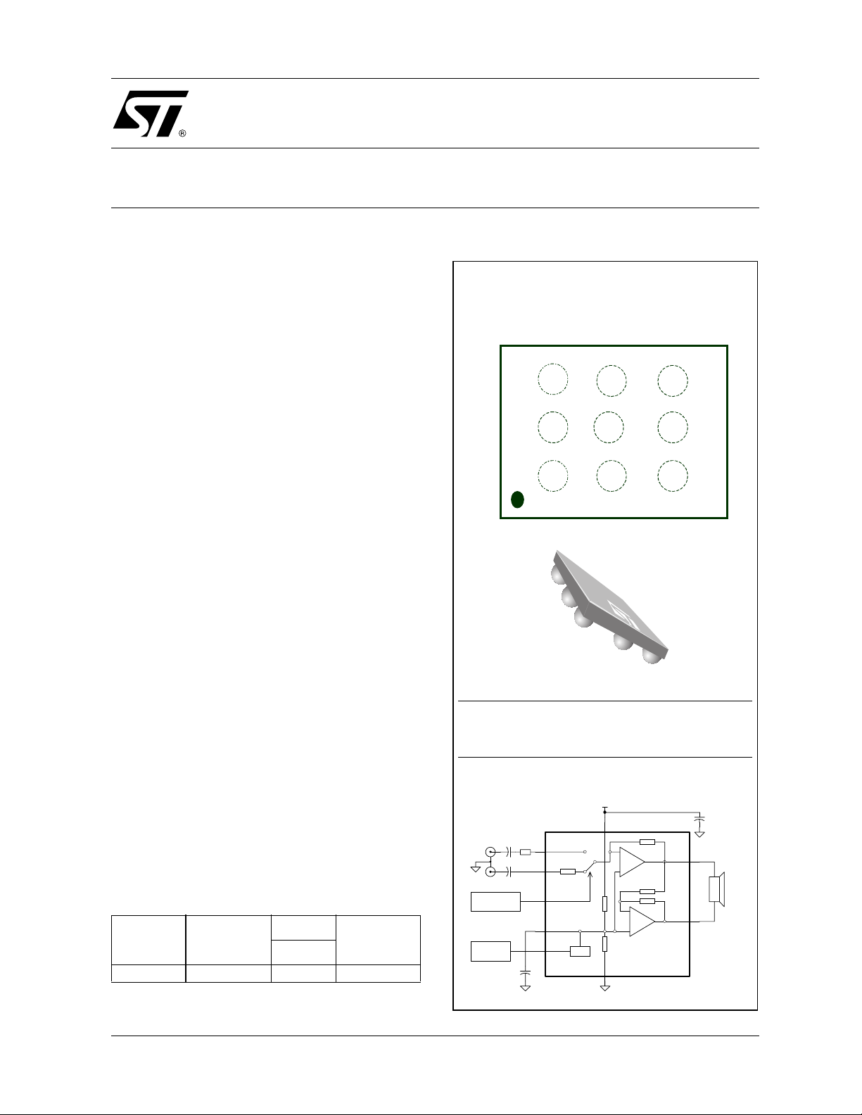
■ FLIP CHIP PACKAGE 9 x 300µm bumps
DESCRIPTION
At 3.3v, the TS4973 is an Audio Power Ampl ifier
capable of delivering 400m W of continuous RMS
ouput power into a 8
THD+N, and 30mW( typ ) per channel of continuous average power into stereo 32
0.5% THD+N from 20Hz to 20kHz. An external
standby mode co ntrol reduces the supply current
to less than 10nA. An internal over-temperature
shutdown protection is provided.
The TS4973 has been designed for high quality
audio applications such as m obile phones and t o
minimize the number of external components. It
has two inputs which can be used to switch the
gain between 6dB ( internal ) o r a user’s adjustable gain setting with one external resitance.
APPLICATIONS
■Mobile Phones (Cellular / Cordless)
■PDAs
■Laptop/Notebook computers
■Portable Audio Devices
ORDER CODE
Part
Number
TS4973IJT -40, +85°C
J = Flip Chip Package - only available in Tape & Reel (JT))
February 2003
This is a preliminary information on a new product now in development. Details are subject to change without notice.
Temperature
Range
= 2.8V to 5.5V
CC
Ω bridged-tied loads with 1%
Ω BTL loads with
Package
Marking
J
•
A73
PIN CONNECTIONS (top view)
TS4973IJT - FLIP CHIP
Vin2
Vin2
VOUT1 GS
VOUT1 GS
Vin1 GND BYPASS
Vin1 GND BYPASS
TYPICAL APPLICATION SCHEMATIC
Cin1
threshold = 0.9V
Cin2
Rin
1
7
9 Gain Setting
3
5
Cb
In1
In2
Bypass
Standby
Audio
Inputs
Gain Setting level
Standby level
threshold = 0.9V
VCC
VCC
VCC
6
VCCGND
-
+
AV = -1
+
Bias
2
STBY
STBY
VOUT2
VOUT2
Vout 1
Vout 2
TS4973
Cs
8
RL
8 Ohms
4
1/9
TS4973
ABSOLUTE MAXIMUM RATINGS
Symbol Parameter Value Unit
V
T
T
R
Supply voltage
CC
V
Input Voltage
i
Operating Free Air Temperature Range -40 to + 85 °C
oper
Storage Temperature -65 to +150 °C
stg
T
Maximum Junction Temperature 150 °C
j
Thermal Resistance Junction to Ambient
thja
Pd Power Dissipation
ESD Human Body Model 2 kV
ESD Machine Model 200 V
Latch-up Latch-up Immunity 200 mA
Lead Temperature (soldering, 10sec ) 250 °C
1. All voltages values are measured with respect to the ground pin.
2. The magnitude of input signal must never exceed V
3. Device is protected in case of over temperature by a thermal shutdown active @ 150°C.
4. Exceeding the power derating curves during a long period, involves abnormal operating condition.
OPERATING CONDITIONS
Symbol Parameter Value Unit
V
V
V
V
R
1. With Heat Sink Surface = 125mm2
Supply Voltage 2.8 to 5.5 V
CC
Common Mode Input Voltage Range
ICM
Standby Voltage Input :
STB
Device ON
Device OFF
Gain Setting Voltage Input :
GS
External Gain (In1 Input)
Internal Gain (In2 Input)
R
Load Resistor 4 - 32
L
Thermal Resistance Junction to Ambient
thja
1)
2)
3)
Internally Limited
+ 0.3V / GND - 0.3V
CC
G
1.5 ≤ V
GND ≤ V
1.5 ≤ V
GND ≤ V
1)
6V
GND to V
CC
200 °C/W
4)
to VCC - 1.5V
ND
≤ V
STB
CC
≤ 0.4
STB
≤ V
STB
CC
≤ 0.4
STB
90 °C/W
V
V
V
V
Ω
2/9
TS4973
ELECTRICAL CHARACTERISTICS
V
= +5V, GND = 0V , T
CC
Symbol Parameter Min. Typ. Max. Unit
= 25°C (unless otherwise specified)
amb
I
CC
I
STANDBY
Voo
Po
BTL GAIN
THD + N
PSRR
Supply Current
No input signal, no load
Standby Current
No input signal, Vstdby = Gnd, RL = 8
1)
Ω
Output Offset Voltage
No input signal, RL = 8
Ω
Output Power
THD = 1% Max, f = 1kHz, RL = 8
Ω
GS = Low
input signal Vin = 100mV rms, RL = 8
Ω
Total Harmonic Distortion + Noise
Po = 250mW rms, GS = Low, 20Hz < f < 20kHz, RL = 8
Power Supply Rejection Ratio
F = 217Hz, RL = 8
2)
GS = Low
Ω,
Vripple = 200mV rms
,
68mA
10 1000 nA
520mV
0.85 1.2 W
5.6 6 6.4 dB
Ω
0.1 %
50 53 dB
Input Grounded, Cin = 220nF, Cb = 1µF
3)
GS = Low
Ω,
Vripple = 200mV rms
,
75 dB
PSRR
Power Supply Rejection Ratio
F = 217Hz, RL = 8
Input floating, Cb = 1µF
Zin
Input Impedance
GS = Low
37.5 50 62.5 K
Rfeed Internal Feedback Resistor 37.5 50 62.5 K
Φ
GM
GBP
1. Standby mode is actived wh en Vstdby is tied to Gnd
2. Dynamic mea surements - 20*log(rms(Vout )/ rms(Vri ppl e)). Vripple is an added sinus signal to Vcc @ f = 217Hz
3. Dynamic mea surements - 20*log(rms(Vout )/ rms(Vri ppl e)). Vripple is an added sinus signal to Vcc @ f = 217Hz
Phase Margin at GS = Low
M
R
= 8Ω, CL = 500pF
L
Gain Margin
R
= 8Ω, CL = 500pF
L
Gain Bandwidth Product
R
= 8
L
70 Degrees
20 dB
Ω
2MHz
Ω
Ω
3/9

TS4973
ELECTRICAL CHARACTERISTICS
V
= +3.3V, GND = 0V, T
CC
Symbol Parameter Min. Typ. Max. Unit
= 25°C (unless otherwise specified)4)
amb
I
CC
I
STANDBY
Voo
Po
BTL GAIN
THD + N
PSRR
Supply Current
No input signal, no load
Standby Current
1)
No input signal, Vstdby = Vcc, RL = 8
Output Offset Voltage
No input signal, RL = 8
Ω
Output Power
THD = 1% Max, f = 1kHz, RL = 8
Ω
GS = Low
input signal Vin = 100mV rms, RL = 8
Total Harmonic Distortion + Noise
Po = 250mW rms, Gv = 2, 20Hz < f < 20kHz, RL = 8
Power Supply Rejection Ratio
f = 217Hz, RL = 8
GS = Low
Ω,
2)
Vripple = 200mV rms
,
5.5 8 mA
Ω
10 1000 nA
520mV
350 500 mW
Ω
Ω
5.6 6 6.4 dB
0.1 %
50 53 dB
Input Grounded, Cin = 220nF, Cb = 1µF
PSRR
Power Supply Rejection Ratio
f = 217Hz, RL = 8
GS = Low
Ω,
3)
Vripple = 200mV rms
,
75 dB
Input floating, Cb = 1µF
Zin
Input Impedance
GS = Low
37.5 50 62.5 K
Rfeed Internal Feedback Resistor 37.5 50 62.5 K
Φ
GM
GBP
1. Standby mode i s actived when Vstdby is tied to Vcc
2. Dynamic mea surements - 20*log(rms(Vout )/ rms(Vri ppl e)). Vripple is an added sinus signal to Vcc @ f = 217Hz
3. Dynamic mea surements - 20*log(rms(Vout )/ rms(Vri ppl e)). Vripple is an added sinus signal to Vcc @ f = 217Hz
4. All electrical values are made by correlation between 2.8V and 5V measurements
Phase Margin at Unity Gain
M
R
= 8Ω, CL = 500pF
L
Gain Margin
R
= 8Ω, CL = 500pF
L
Gain Bandwidth Product
R
= 8
L
70 Degrees
20 dB
Ω
2MHz
Ω
Ω
4/9

ELECTRICAL CHARACTERISTICS
V
= 2.8V, GND = 0V, T
CC
Symbol Parameter Min. Typ. Max. Unit
= 25°C (unless otherwise specified)
amb
TS4973
I
CC
I
STANDBY
Voo
BTL GAIN
Po
THD + N
PSRR
Supply Current
No input signal, no load
Standby Current
1)
No input signal, Vstdby = Vcc, RL = 8
Output Offset Voltage
No input signal, RL = 8
Ω
GS = Low
input signal Vin = 100mV rms, RL = 8
Output Power
THD = 1% Max, f = 1kHz, RL = 8
Ω
Total Harmonic Distortion + Noise
Po = 200mW rms, Gv = 2, 20Hz < f < 20kHz, RL = 8
Power Supply Rejection Ratio
F = 217Hz, RL = 8
2)
GS = Low
Ω,
Vripple = 200mV rms
,
5.5 8 mA
Ω
10 1000 nA
520mV
Ω
5.6 6 6.4 dB
250 350 mW
Ω
0.1 %
50 53 dB
Input Grounded, Cin = 220nF, Cb = 1µF
3)
GS = Low, Vripple = 200mV rms
Ω,
75 dB
PSRR
Power Supply Rejection Ratio
F = 217Hz, RL = 8
Input Floating, Cb = 1µF
Zin
Input Impedance
GS = Low
37.5 50 62.5 K
Rfeed Internal Feedback Resistor 37.5 50 62.5 K
Φ
GM
GBP
1. Standby mode is actived wh en Vstdby is tied to Gnd
2. Dynamic mea surements - 20*log(rms(Vout )/ rms(Vri ppl e)). Vripple is an added sinus signal to Vcc @ F = 217Hz
3. Dynamic mea surements - 20*log(rms(Vout )/ rms(Vri ppl e)). Vripple is an added sinus signal to Vcc @ F = 217Hz
Phase Margin at Unity Gain
M
R
= 8Ω, CL = 500pF
L
Gain Margin
R
= 8Ω, CL = 500pF
L
Gain Bandwidth Product
R
= 8
L
70 Degrees
20 dB
Ω
2MHz
Ω
Ω
5/9

TS4973
Components Functional Description
Inverting input resistor which sets the closed loop gain ( when GS = high) in conjunction with the inter-
Rin
Cin1 Input coupling capacitor which blocks the DC voltage at the amplifier input terminal In1
Cin2
Cs Supply Bypass capacitor which provides power supply filtering (Recommended value = 1µF)
Cb Bypass pin capacitor which provides half supply filtering (Recommended value = 1µF)
Gv
REMARKS
1. All measurements, except PSRR measurements, are made with a supply bypass capacitor Cs = 1µF.
2. The standby response time is about 1µs.
nal feedback resistor Rfeed. This resistor also forms a high pass filter with Cin1
Fc = 1 / (2 x Pi x Rin x Cin1)
Input coupling capacitor which blocks the DC voltage at the amplifier input terminal In2. This capacitor
also forms a high pass filter with Zin (internal input impedance when Gs = Low
Fc = 1 / (2 x Pi x Zin x Cin2)
Closed loop gain in BTL configuration
When Gs = Low, Gv = 2 or 6dB
When GS = high, Gv = 2 x (Rfeed / Rin). Rfeed value see Electrical Characteristics.
6/9

TS4973
DAISY CHAIN MECHANICAL DATA ( Top View : all drawings dimensions are in millimeters )
3
3
2
2
1
1
REMARKS
Daisy chain sample is featuring pins connection two by two. The schematic above is illustrating the way
connecting pins each other. This sample is used for testing continuity on board. PCB needs to be designed
on the opposite way, where pin connections are not done on daisy chain samples. By that way, just
connecting an Ohmeter between pin 8 and pin 1, the soldering process continuity can be tested.
Vn2
Vn2
Vout1
Vout1
Vout1
Vout1
Vn1 Gnd Bypass
Vn1 Gnd Bypass
In1
In1
A
A
Vcc
Vcc
GS
GS
GS
GS
Gnd
Gnd
B
B
2.26 mm
2.26 mm
2.26 mm
2.26 mm
9
9
Stdby
Stdby
StdbyVccIn2
StdbyVccIn2
Vout2
Vout2
Vout2
Vout2
Bypass
Bypass
C
C
1.6 mm
1.6 mm
1.6 mm
1.6 mm
ORDER CODE
Part Number
TSDC05IJT -40, +85°C
Temperature
Range
TS4973 Footprint Recommendation
Φ
=250µm
Φ
m
µ
500
m
µ
500
=400µm
Package
J
•
500µm
Marking
DC5
500
150
75µm min.
µ
100
µ
m min.
m max.
Track
µ
m
Solder mask opening
Pad in Cu 35µm with Flash NiAu (6µm, 0.15µm)
7/9

TS4973
PIN OUT (top view) MARKING (top view)
Vin2
1
1
3
3
2
2
Vin2
VOUT1 GS
VOUT1 GS
Vin1 GND BYPASS
Vin1 GND BYPASS
VCC
VCC
STBY
STBY
VOUT2
VOUT2
A73
A73
YWW
YWW
■ Balls are underneath
B
A
A
PACKAGE MECHANICAL DATA
FLIP CHIP - 9 BU MPS
0.5mm
0.5mm
B
2.26 mm
2.26 mm
0.5mm
0.5mm
C
C
∅ 0.25mm
∅ 0.25mm
■ Logo : ST
■ Part Number : A73
■ Date Code : YWW
■ The Dot is for marking pin A1
1.6 mm
1.6 mm
■ Die size : 2.26mm x 1.6mm ( ±10%)
■ Die height (including bumps) : 600µm
±30µm
■ Bumps diameter : 300µm ±15µm
■ Pitch: 500µm ±10µm
8/9
600µm
600µm

TAPE & REEL SPECIFICATION ( top view )
1
1
A
A1A
A
A1A
TS4973
1
1
User direction of feed User direction of feed
User direction of feed User direction of feed
Information furnished is belie ved to be accurate and reliable. However, STMicroelec tronics assumes no responsibility for the
consequences of use of such information nor for any infringement of patents or other rights of third parties which may result from
its use. No license is granted by implication or otherwise under any patent or patent rights of STMicroelectronics. Specifications
mentioned in this publicat ion are subject to change without notice. Thi s publication supersedes and replaces all information
previously supplied. STMicro electronics products are not a uthorized for use as critical c omponents in life support de vices or
systems without express written approval of STMicroelectronics.
The ST logo is a registered trademark of STMicroelectronics
© 2003 STM icroelectronics - A ll Rights Reserved
STMicroelectronics GROUP OF COMPANI E S
Australi a - Brazil - Ch i na - F i nland - France - Germany - Hong Kong - India - Italy - Japan - M al aysia - Malta - Morocco
Singapore - Spain - Sweden - Switzerland - United Kingdom
http://www.st.com
9/9
 Loading...