

SGS Thomson Microelectronics TS4973IJT, TS4973 Datasheet
TS4973
1.2W TWO AUDIO INPUTS WITH GAIN CONTROL POWER
AMPLIFIER WITH STANDBY MODE ACTIVE LOW
ADVANCE DATA
■OPERATING FROM V
■RAIL TO RAIL OUTPUT
■1.2W OUTPUT POWER @ Vcc=5V, THD=1%,
F=1kHz, with 8Ω Load
■ULTRA LOW CONSUMPTION IN STANDBY
MODE (10nA)
■53dB PSRR @ 217Hz from 2.8 to 5V
■ LOW POP & CLICK
■ULTRA LOW DISTORTION (0.05%)
■ GAIN SETTINGS PIN : GS
■UNITY GAIN STABLE
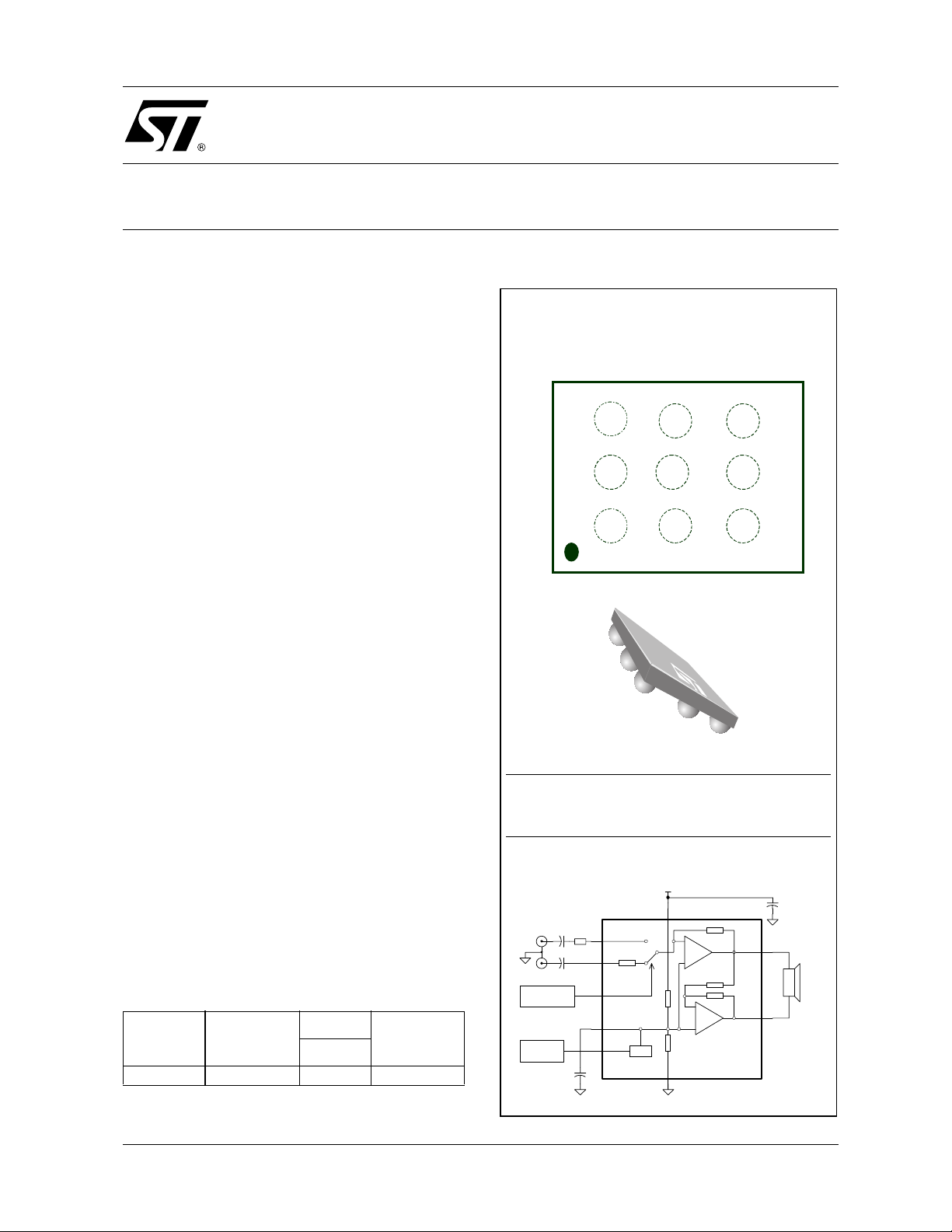
■ FLIP CHIP PACKAGE 9 x 300µm bumps
DESCRIPTION
At 3.3v, the TS4973 is an Audio Power Ampl ifier
capable of delivering 400m W of continuous RMS
ouput power into a 8
THD+N, and 30mW( typ ) per channel of continuous average power into stereo 32
0.5% THD+N from 20Hz to 20kHz. An external
standby mode co ntrol reduces the supply current
to less than 10nA. An internal over-temperature
shutdown protection is provided.
The TS4973 has been designed for high quality
audio applications such as m obile phones and t o
minimize the number of external components. It
has two inputs which can be used to switch the
gain between 6dB ( internal ) o r a user’s adjustable gain setting with one external resitance.
APPLICATIONS
■Mobile Phones (Cellular / Cordless)
■PDAs
■Laptop/Notebook computers
■Portable Audio Devices
ORDER CODE
Part
Number
TS4973IJT -40, +85°C
J = Flip Chip Package - only available in Tape & Reel (JT))
February 2003
This is a preliminary information on a new product now in development. Details are subject to change without notice.
Temperature
Range
= 2.8V to 5.5V
CC
Ω bridged-tied loads with 1%
Ω BTL loads with
Package
Marking
J
•
A73
PIN CONNECTIONS (top view)
TS4973IJT - FLIP CHIP
Vin2
Vin2
VOUT1 GS
VOUT1 GS
Vin1 GND BYPASS
Vin1 GND BYPASS
TYPICAL APPLICATION SCHEMATIC
Cin1
threshold = 0.9V
Cin2
Rin
1
7
9 Gain Setting
3
5
Cb
In1
In2
Bypass
Standby
Audio
Inputs
Gain Setting level
Standby level
threshold = 0.9V
VCC
VCC
VCC
6
VCCGND
-
+
AV = -1
+
Bias
2
STBY
STBY
VOUT2
VOUT2
Vout 1
Vout 2
TS4973
Cs
8
RL
8 Ohms
4
1/9
TS4973
ABSOLUTE MAXIMUM RATINGS
Symbol Parameter Value Unit
V
T
T
R
Supply voltage
CC
V
Input Voltage
i
Operating Free Air Temperature Range -40 to + 85 °C
oper
Storage Temperature -65 to +150 °C
stg
T
Maximum Junction Temperature 150 °C
j
Thermal Resistance Junction to Ambient
thja
Pd Power Dissipation
ESD Human Body Model 2 kV
ESD Machine Model 200 V
Latch-up Latch-up Immunity 200 mA
Lead Temperature (soldering, 10sec ) 250 °C
1. All voltages values are measured with respect to the ground pin.
2. The magnitude of input signal must never exceed V
3. Device is protected in case of over temperature by a thermal shutdown active @ 150°C.
4. Exceeding the power derating curves during a long period, involves abnormal operating condition.
OPERATING CONDITIONS
Symbol Parameter Value Unit
V
V
V
V
R
1. With Heat Sink Surface = 125mm2
Supply Voltage 2.8 to 5.5 V
CC
Common Mode Input Voltage Range
ICM
Standby Voltage Input :
STB
Device ON
Device OFF
Gain Setting Voltage Input :
GS
External Gain (In1 Input)
Internal Gain (In2 Input)
R
Load Resistor 4 - 32
L
Thermal Resistance Junction to Ambient
thja
1)
2)
3)
Internally Limited
+ 0.3V / GND - 0.3V
CC
G
1.5 ≤ V
GND ≤ V
1.5 ≤ V
GND ≤ V
1)
6V
GND to V
CC
200 °C/W
4)
to VCC - 1.5V
ND
≤ V
STB
CC
≤ 0.4
STB
≤ V
STB
CC
≤ 0.4
STB
90 °C/W
V
V
V
V
Ω
2/9
TS4973
ELECTRICAL CHARACTERISTICS
V
= +5V, GND = 0V , T
CC
Symbol Parameter Min. Typ. Max. Unit
= 25°C (unless otherwise specified)
amb
I
CC
I
STANDBY
Voo
Po
BTL GAIN
THD + N
PSRR
Supply Current
No input signal, no load
Standby Current
No input signal, Vstdby = Gnd, RL = 8
1)
Ω
Output Offset Voltage
No input signal, RL = 8
Ω
Output Power
THD = 1% Max, f = 1kHz, RL = 8
Ω
GS = Low
input signal Vin = 100mV rms, RL = 8
Ω
Total Harmonic Distortion + Noise
Po = 250mW rms, GS = Low, 20Hz < f < 20kHz, RL = 8
Power Supply Rejection Ratio
F = 217Hz, RL = 8
2)
GS = Low
Ω,
Vripple = 200mV rms
,
68mA
10 1000 nA
520mV
0.85 1.2 W
5.6 6 6.4 dB
Ω
0.1 %
50 53 dB
Input Grounded, Cin = 220nF, Cb = 1µF
3)
GS = Low
Ω,
Vripple = 200mV rms
,
75 dB
PSRR
Power Supply Rejection Ratio
F = 217Hz, RL = 8
Input floating, Cb = 1µF
Zin
Input Impedance
GS = Low
37.5 50 62.5 K
Rfeed Internal Feedback Resistor 37.5 50 62.5 K
Φ
GM
GBP
1. Standby mode is actived wh en Vstdby is tied to Gnd
2. Dynamic mea surements - 20*log(rms(Vout )/ rms(Vri ppl e)). Vripple is an added sinus signal to Vcc @ f = 217Hz
3. Dynamic mea surements - 20*log(rms(Vout )/ rms(Vri ppl e)). Vripple is an added sinus signal to Vcc @ f = 217Hz
Phase Margin at GS = Low
M
R
= 8Ω, CL = 500pF
L
Gain Margin
R
= 8Ω, CL = 500pF
L
Gain Bandwidth Product
R
= 8
L
70 Degrees
20 dB
Ω
2MHz
Ω
Ω
3/9
 Loading...