

SGS Thomson Microelectronics TS4900IST, TS4900IDT, TS4900ID, TS4900 Datasheet
TS4900
300mW at 3.3V SUPPLY AUDIO POWER AMPLIFIER
WITH STANDBY MODE ACTIVE HIGH
■OPERATING FROM V
= 2.5V to 5.5V
CC
■0.7W OUTPUT POWER @ Vcc=5V, THD=1%,
f=1kHz, with an 8
Ω load
■0.3W OUTPUT POWER @ Vcc=3.3V,
THD=1%, f=1kHz, with an 8
Ω load
■ULTRA LOW CONSUMPTION IN STANDBY
MODE (10nA)
■75dB PSRR @ 217Hz from 5V to 2.6V
■ULTRA LOW POP & CLICK
■ULTRA LOW DISTORTION (0.1%)
■UNITY GAIN STABLE
■AVAILABLE IN MiniSO8 & SO8
DESCRIPTION
The TS4900 is an audio power amplifier designed
to provide the best pri ce to power ratio while preserving high audio quality.
Available in MiniSO8 & SO8 package, it is capable
of delivering up to 0.7W of continuous RMS ouput
power into an 8
TS4900 is also exhibiting an outstanding 0.1%
distortion level (THD) from a 5V supply for a Pout
of 200mW RMS.
Ω load @ 5V.
PIN CONNECTIONS (top view)
TS4900IST - MiniSO8
Standby
Bypass
V+
Standby
Bypass
V+
VIN-
1
2
3
IN
4
VIN-
TS4900ID-TS4900IDT - SO8
1
2
3
IN
4
8
V2OUT
7
GND
6
CC
V
5
VOUT1
8
V2OUT
7
GND
6
CC
V
5
VOUT1
An externally controlle d standby m ode control reduces the supply current to less than 10nA. It also
includes an internal thermal shutdown protection.
The unity-gain stable amplifier can be configured
by external gain setting resistors.
APPLICATIONS
■Mobile Phones (Cellular / Cordless)
■PDAs
■Portable Audio Devices
ORDER CODE
Part Number
TS4900IS
TS4900ID
S = MiniSO Package (MiniSO) only available in Tape & Reel (ST)
D = Small Outline Package (SO) - also available in Tape & Reel (DT)
Temperature
Range
-40, +85°C
January 2002
Package
SD
•
•
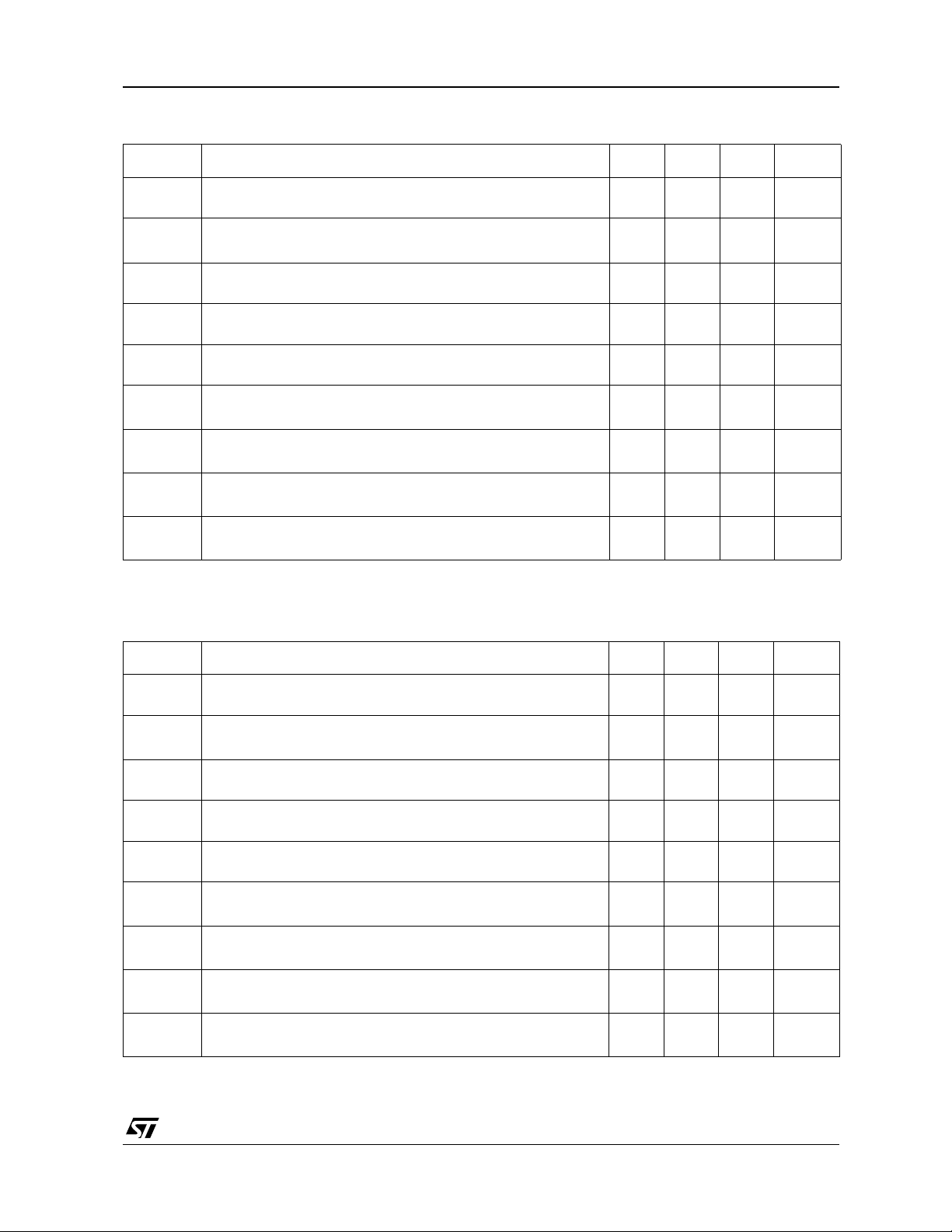
TYPICAL APPLICATION SCHEMATIC
1/19
TS4900
ABSOLUTE MAXIMUM RATINGS
Symbol Parameter Value Unit
V
T
T
R
Supply voltage
CC
V
Input Voltage
i
Operating Free Air Temperature Range -40 to + 85 °C
oper
Storage Temperature -65 to +150 °C
stg
T
Maximum Junction Temperature 150 °C
j
Thermal Resistance Junction to Ambient
thja
SO8
MiniSO8
Pd Power Dissipation
ESD Human Body Model 2 kV
ESD Machine Model 200 V
Latch-up Latch-up Immunity Class A
Lead Temperature (soldering, 10sec ) 250 °C
1. All voltages values are measured with respect to the ground pin.
2. The magnitude of input signal must never exceed V
3. Device is protected in case of over temperature by a thermal shutdown active @ 150°C.
4. Exceeding the power derating curves during a long period, will cause abnormal operation.
OPERATING CONDITIONS
1)
2)
3)
6V
GND to V
CC
175
215
4)
+ 0.3V / GND - 0.3V
CC
Internally Limited
V
°C/W
Symbol Parameter Value Unit
V
V
Supply Voltage 2.5 to 5.5 V
CC
to VCC - 1.5V
Common Mode Input Voltage Range
ICM
G
ND
Standby Voltage Input :
≤ V
V
STB
Device ON
Device OFF
R
Load Resistor 4 - 32
L
R
Thermal Resistance Junction to Ambient
thja
1)
SO8
MiniSO8
1. This thermal resistance can be reduced with a suitable PCB layout (see Power Derating Curves)
G
V
- 0.5V ≤ V
CC
ND
STB
150
190
≤ 0.5V
≤ V
STB
CC
V
V
Ω
°C/W
2/19
TS4900
ELECTRICAL CHARACTERISTICS
= +5V, GND = 0V , T
V
CC
Symbol Parameter Min. Typ. Max. Unit
= 25°C (unless otherwise specified)
amb
I
CC
I
STANDBY
Voo
Po
THD + N
PSRR
Φ
GM
GBP
1. Standby mode i s actived when Vstdby is tied to Vcc
2. Dynamic measurements - 20*log(r m s(Vout)/rms(Vripple)). Vripple is the surim posed sinus signal to Vc c @ f = 217Hz
= +3.3V, GND = 0V, T
V
CC
Supply Current
No input signal, no load
Standby Current
1)
No input signal, Vstdby = Vcc, RL = 8
Output Offset Voltage
No input signal, RL = 8
Output Power
THD = 1% Max, f = 1kHz, RL = 8
Total Harmonic Distortion + Noise
Po = 250mW rms, Gv = 2, 20Hz < f < 20kHz, RL = 8
Power Supply Rejection Ratio
f = 217Hz, RL = 8
Phase Margin at Unity Gain
M
R
= 8Ω, CL = 500pF
L
Gain Margin
R
= 8Ω, CL = 500pF
L
Gain Bandwidth Product
R
= 8
Ω
L
amb
Ω
Ω
Ω
Ω
2)
RFeed = 22K
Ω,
Vripple = 200mV rms
Ω,
= 25°C (unless otherwise specified)3)
68mA
10 1000 nA
520mV
0.7 W
0.15 %
75 dB
70 Degrees
20 dB
2MHz
Symbol Parameter Min. Typ. Max. Unit
I
CC
I
STANDBY
Voo
Po
THD + N
PSRR
Φ
GM
GBP
1. Standby mode i s actived when Vstdby is tied to Vcc
2. Dynamic measurements - 20*log(r m s(Vout)/rms(Vripple)). Vripple is the surim posed sinus signal to Vc c @ f = 217Hz
3. All electrical values are made by correlation between 2.6V and 5V measurement s
Supply Current
No input signal, no load
Standby Current
1)
No input signal, Vstdby = Vcc, RL = 8
Output Offset Voltage
No input signal, RL = 8
Output Power
THD = 1% Max, f = 1kHz, RL = 8
Total Harmonic Distortion + Noise
Po = 250mW rms, Gv = 2, 20Hz < f < 20kHz, RL = 8
Power Supply Rejection Ratio
f = 217Hz, RL = 8
Phase Margin at Unity Gain
M
R
= 8Ω, CL = 500pF
L
Gain Margin
R
= 8Ω, CL = 500pF
L
Gain Bandwidth Product
R
= 8
Ω
L
Ω
2)
RFeed = 22K
Ω,
Ω
Ω
Vripple = 200mV rms
Ω,
5.5 8 mA
10 1000 nA
520mV
300 mW
Ω
0.15 %
75 dB
70 Degrees
20 dB
2MHz
3/19
TS4900
ELECTRICAL CHARACTERISTICS
V
= 2.6V, GND = 0V, T
CC
Symbol Parameter Min. Typ. Max. Unit
= 25°C (unless otherwise specified)
amb
I
CC
I
STANDBY
Voo
Po
THD + N
PSRR
Φ
GM
GBP
1. Standby mode i s actived when Vstdby is tied to Vcc
2. Dynamic measurements - 20*log(r m s(Vout)/rms(Vripple)). Vripple is the surim posed sinus signal to Vc c @ f = 217Hz
Supply Current
No input signal, no load
Standby Current
1)
No input signal, Vstdby = Vcc, RL = 8
Output Offset Voltage
No input signal, RL = 8
Output Power
THD = 1% Max, f = 1kHz, RL = 8
Total Harmonic Distortion + Noise
Po = 200mW rms, Gv = 2, 20Hz < f < 20kHz, RL = 8
Power Supply Rejection Ratio
f = 217Hz, RL = 8
Phase Margin at Unity Gain
M
R
= 8Ω, CL = 500pF
L
Gain Margin
R
= 8Ω, CL = 500pF
L
Gain Bandwidth Product
R
= 8
Ω
L
Ω
2)
RFeed = 22K
Ω,
Ω
Ω
Vripple = 200mV rms
Ω,
5.5 8 mA
10 1000 nA
520mV
180 mW
Ω
0.15 %
75 dB
70 Degrees
20 dB
2MHz
Components Functional Description
Rin
Cin
Inverting input resistor which sets the closed loop gain in conjunction with Rfeed. This resistor also
forms a high pass filter with Cin (fc = 1 / (2 x Pi x Rin x Cin))
Input coupling capacitor which blocks the DC voltage at the amplifier input terminal
Rfeed Feed back resistor which sets the closed loop gain in conjunction with Rin
Cs Supply Bypass capacitor which provides power supply filtering
Cb Bypass pin capacitor which provides half supply filtering
Cfeed
Low pass filter capacitor allowing to cut the high frequency
(low pass filter cut-off frequency 1 / (2 x Pi x Rfeed x Cfeed))
Rstb Pull-up resistor which fixes the right supply level on the standby pin
Gv Closed loop gain in BTL configuration = 2 x (Rfeed / Rin)
REMARKS
1. All measurements, except PSRR measurements, are made with a supply bypass capacitor Cs = 100µF.
2. The standby response time is about 1µs.
4/19
TS4900
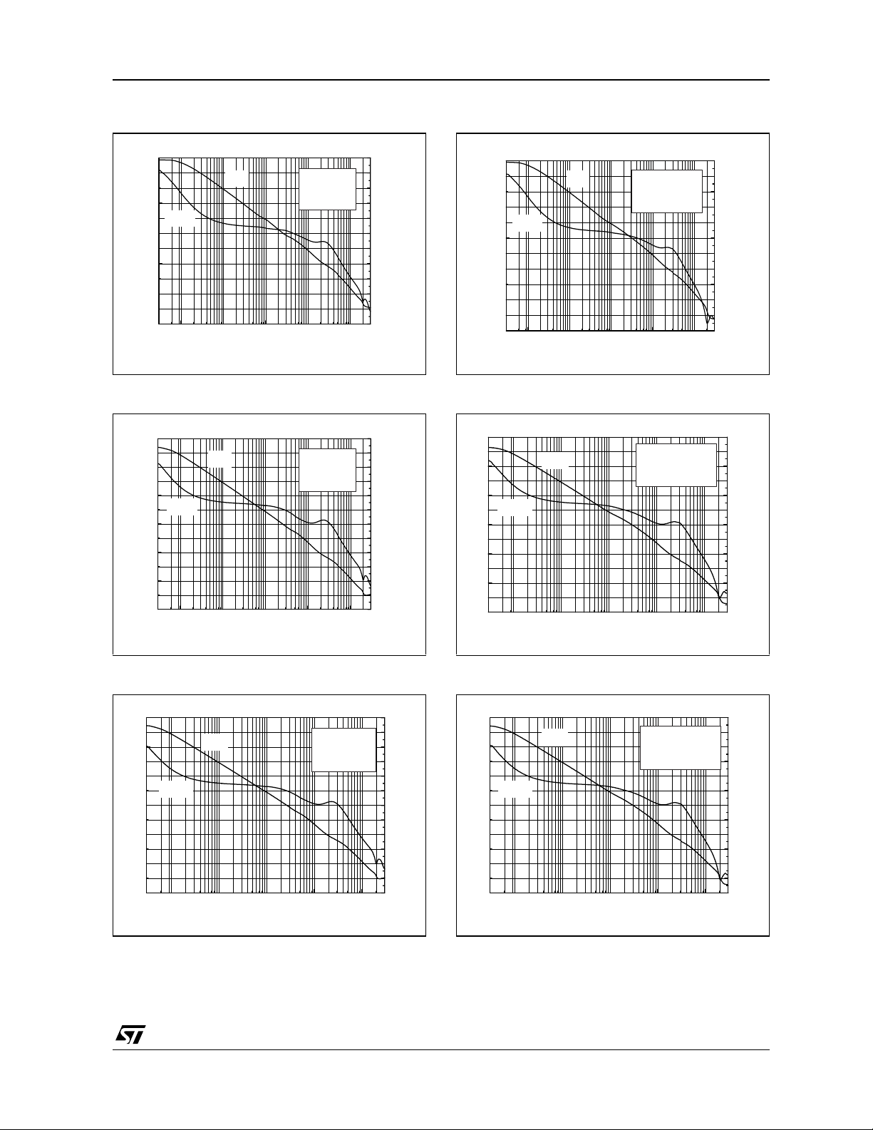
0.3 1 10 100 1000 10000
-40
-20
0
20
40
60
80
-240
-220
-200
-180
-160
-140
-120
-100
-80
-60
-40
-20
0
Gain (dB)
Frequency (kHz)
Vcc = 3.3V
ZL = 8Ω + 560pF
Tamb = 25°C
Gain
Phase
Phase (Deg)
0.3 1 10 100 1000 10000
-40
-20
0
20
40
60
80
-240
-220
-200
-180
-160
-140
-120
-100
-80
-60
-40
-20
0
Gain (dB)
Frequency (kHz)
Vcc = 2.6V
ZL = 8Ω + 560pF
Tamb = 25°C
Gain
Phase
Phase (Deg)
Fig. 1 : Open Loop Frequency Response
0
60
40
Phase
20
Gain (dB)
0
-20
-40
0.3 1 10 100 1000 10000
Gain
Frequency (kHz)
Vcc = 5V
RL = 8
Tamb = 25°C
Ω
-20
-40
-60
-80
-100
-120
-140
-160
-180
-200
-220
Fig. 3 : Open Loop Frequency Response
80
60
40
20
Gain (dB)
0
-20
-40
0.3 1 10 100 1000 10000
Gain
Phase
Frequency (kHz)
Vcc = 33V
RL = 8
Ω
Tamb = 25°C
0
-20
-40
-60
-80
-100
-120
-140
-160
-180
-200
-220
-240
Phase (Deg)
Phase (Deg)
Fig. 2 : Open Loop Frequency Response
0
60
40
Phase
20
Gain (dB)
0
-20
-40
0.3 1 10 100 1000 10000
Gain
Frequency (kHz)
Vcc = 5V
ZL = 8Ω + 560pF
Tamb = 25°C
-20
-40
-60
-80
-100
-120
-140
-160
-180
-200
-220
Fig. 4 : Open Loop Frequency Response
Phase (Deg)
Fig. 5 : Open Loop Frequency Response
80
60
40
20
Gain (dB)
0
-20
-40
0.3 1 10 100 1000 10000
Gain
Phase
Frequency (kHz)
Vcc = 2.6V
RL = 8
Tamb = 25°C
Fig. 6 : Open Loop Frequency Response
0
-20
Ω
-40
-60
-80
-100
-120
-140
-160
-180
-200
-220
-240
Phase (Deg)
5/19
TS4900
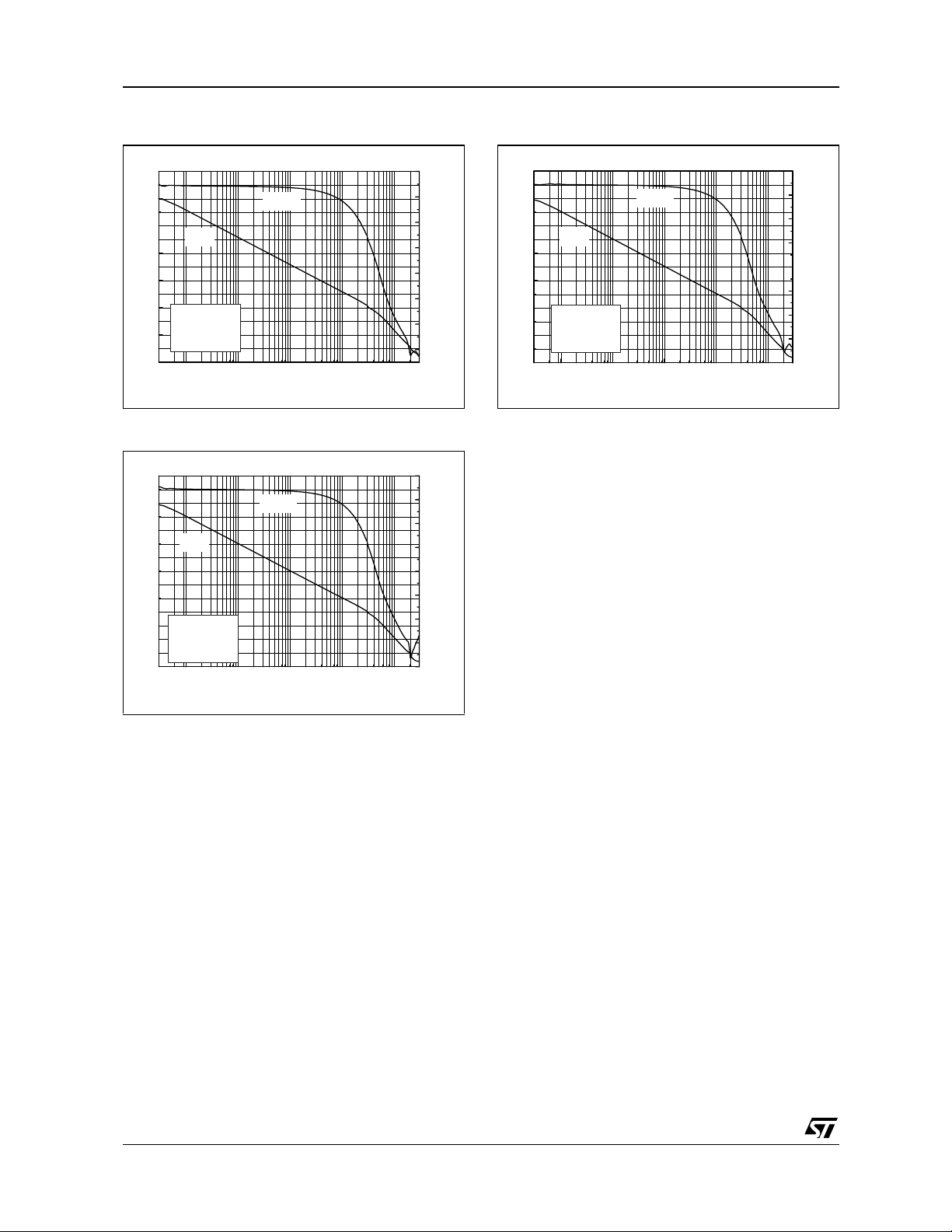
0.3 1 10 100 1000 10000
-40
-20
0
20
40
60
80
100
-240
-220
-200
-180
-160
-140
-120
-100
-80
Gain (dB)
Frequency (kHz)
Vcc = 3.3V
CL = 560pF
Tamb = 25°C
Gain
Phase
Phase (Deg)
Fig. 7 : Open Loop Frequency Response
100
80
60
Gain
40
20
Gain (dB)
0
Vcc = 5V
CL = 560pF
-20
Tamb = 25°C
-40
0.3 1 10 100 1000 10000
Phase
Frequency (kHz)
-80
-100
-120
-140
-160
-180
-200
-220
Fig. 9 : Open Loop Frequency Response
100
80
60
Gain
40
20
Gain (dB)
0
Vcc = 2.6V
-20
CL = 560pF
Tamb = 25°C
-40
0.3 1 10 100 1000 10000
Phase
Frequency (kHz)
-80
-100
-120
-140
-160
-180
-200
-220
-240
Fig. 8 : Open Loop Frequency Response
Phase (Deg)
Phase (Deg)
6/19
 Loading...