

TS4890
RAIL TO RAIL OUTPUT 1W AUDIO POWER AMPLIFIER WITH
STANDBY MODE ACTIVE LOW
■OPERATING FROM V
= 2.2V to 5.5V
CC
■1W RAI L TO RAIL OUTPUT POWER @
Vcc=5V, THD=1%, f=1kHz, with 8
Ω Load
■ULTRA LOW CONSUMPTION IN STANDBY
MODE (10nA)
■75dB PSRR @ 217Hz from 5 to 2.2V
■POP & CLICK REDUCTION CIRCUITRY
■ULTRA LOW DISTORTION (0.1%)
■UNITY GAIN STABLE
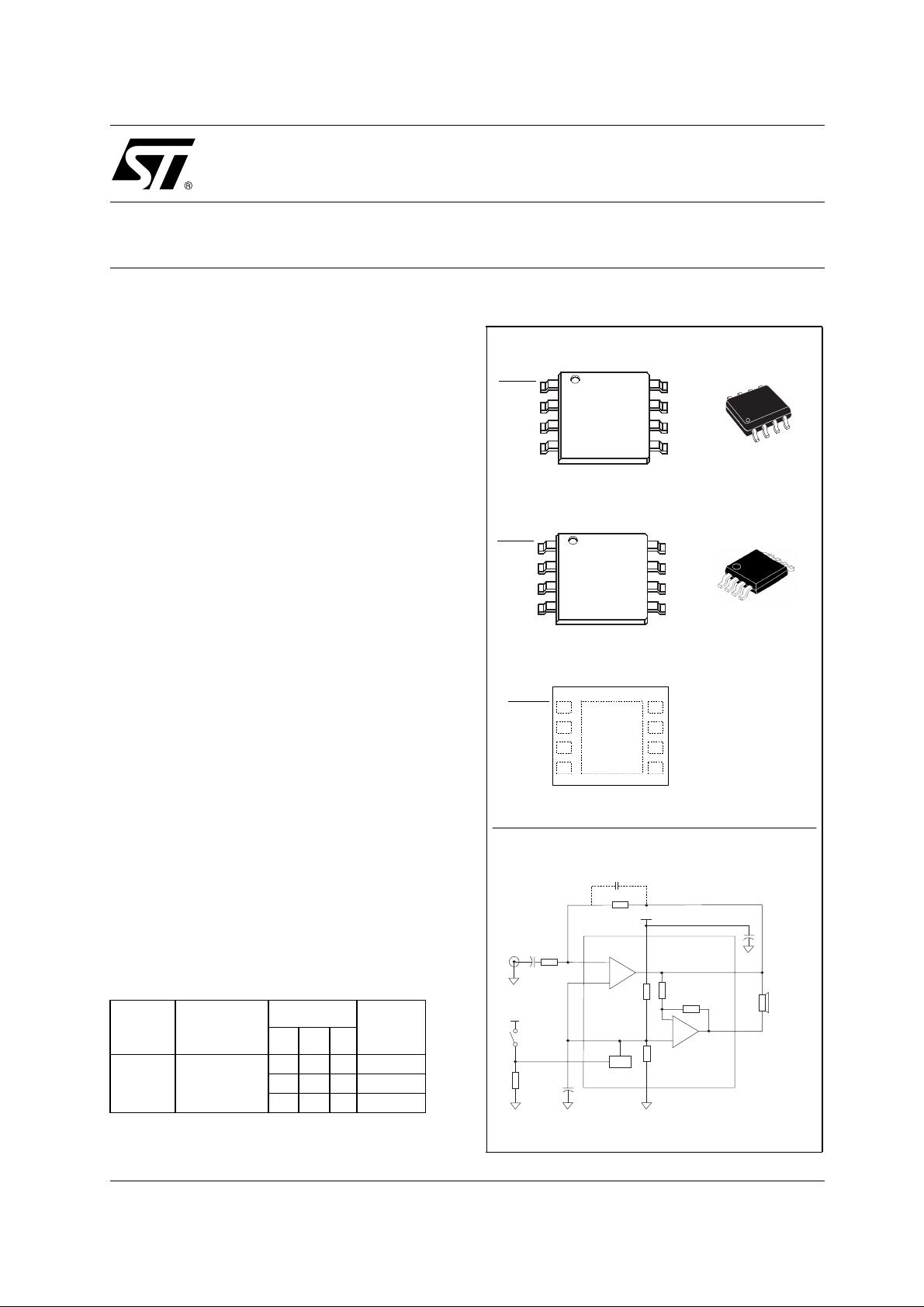
■AVAILABLE IN SO8, MiniSO8 & DFN8
DESCRIPTION
The TS4890 (Min iSO8 & SO 8) is a n A udio P ower
Amplifier capable of delivering 1W of continuous
RMS. ouput power into 8
This Audio Am plifier is exhibiting 0.1% distortion
level (THD) from a 5V supply for a Pout = 250mW
RMS. An external standby mode cont rol reduces
the supply current to less than 10n A. An internal
thermal shutdown protection is also provided.
The TS4890 have b een designed for high quality
audio applications such as m obile phones and t o
minimize the number of external components.
The unity-gain stable amplifier can be configured
by external gain setting resistors.
Ω load @ 5V.
PIN CONNECTIONS (Top View)
TS4890ID, TS4890IDT - SO8
Standby
Bypass
V+
VIN-
Standby
Bypass
V+
IN
VIN-
STANDBY
STANDBY
BYPASS
BYPASS
1
2
3
IN
4
TS4890IST - MiniSO8
1
2
3
4
1
1
2
2
V
V
3
3
IN+
IN+
V
V
4
4
IN-
IN-
8
V2OUT
7
GND
6
CC
V
5
VOUT1
8
V2OUT
7
GND
6
CC
V
5
VOUT1
TS4890IQT - DFN8
V
V
8
8
OUT 2
OUT 2
7
7
GND
GND
6
6
Vcc
Vcc
V
V
5
5
OUT 1
OUT 1
APPLICATIONS
■Mobile Phones (Cellular / Cordless)
■Laptop / Notebook Computers
■PDAs
■Portable Audio Devices
ORDER CODE
Part
Number
Temperature
Range
TS4890 -40, +85°C
MiniSO & DFN only available in Tape & Reel: with T suffix.
SO is available in Tube (D) and of Tape & Reel (DT)
June 2003
Package
Marking
SDQ
•
•
•
4890I
4890
4890
TYPICAL APPLICATION SCHEMATIC
Cfeed
Vcc
Rfeed
Audio
Input
Vcc
Cin
Rstb
Rin
4
Vin-
Vin+
3
Bypass
2
Standby
1
Cb
6
Vcc
-
+
Av=-1
+
Bias
GND
7
Vout1
Vout2
TS4890
Cs
5
RL
8 Ohms
8
1/32
TS4890
ABSOLUTE MAXIMUM RATINGS
Symbol Parameter Value Unit
V
T
T
R
Supply voltage
CC
V
iInput Voltage
Operating Free Air Temperature Range -40 to + 85 °C
oper
Storage Temperature -65 to +150 °C
stg
T
Maximum Junction Temperature 150 °C
j
Thermal Resistance Junction to Ambient
thja
SO8
MiniSO8
DFN8
Pd
Power Dissipation
ESD Human Body Model 2 kV
ESD Machine Model 200 V
Latch-up Immunity Class A
Lead Temperature (solde ring, 10sec ) 260 °C
1. All voltages values are measured with respect to the ground pin.
2. The magnitude of input signal must never exceed V
3. Device is protected in case of over temperature by a thermal shutdown active @ 150°C.
4. Exceeding the power derating curves during a long period may involve abnormal working of the device.
1)
2)
3)
6V
GND to V
CC
175
215
70
4)
+ 0.3V / GND - 0.3V
CC
See Power Derating Curves
Fig. 24
V
°C/W
W
OPERATING CONDITIONS
Symbol Parameter Value Unit
V
V
V
R
1. This thermal resistance can be reduced with a suitable PCB layout (see Power Derating Curves Fig. 24)
2. When mounted o n a 4 l ayers PCB
Supply Voltage 2.2 to 5.5 V
CC
+ 1V to V
Common Mode Input Voltage Range
ICM
G
ND
Standby Voltage Input :
STB
Device ON
Device OFF
R
Load Resistor 4 - 32
L
Thermal Resistance Junction to Ambient
thja
SO8
1)
MiniSO8
2)
DFN8
1.5 ≤ V
G
ND
≤ VCC
STB
V
≤
≤ 0.5
STB
150
190
41
CC
V
V
Ω
°C/W
2/32

TS4890
ELECTRICAL CHARACTERISTICS
= +5V, GND = 0V, T
V
CC
Symbol Parameter Min. Typ. Max. Unit
= 25°C (unless otherwise specified)
amb
I
CC
I
STANDBY
Voo
Po
THD + N
PSRR
Φ
GM
GBP
1. Standby mode is actived wh en Vstdby is tied to GND
2. Dynamic measurements - 20*log(r m s(Vout)/rms(Vripple)). Vripple is the surim posed sinus signal to Vc c @ f = 217Hz
V
= +3.3V, GND = 0V, T
CC
Supply Current
No input signal, no load
Standby Current
1)
No input signal, Vstdby = GND, RL = 8
Output Offset Voltage
No input signal, RL = 8
Output Power
THD = 1% Max, f = 1kHz, RL = 8
Total Harmonic Distortion + Noise
Po = 250mW rms, Gv = 2, 20Hz < f < 20kHz, RL = 8
Power Supply Rejection Ratio
f = 217Hz, RL = 8
Phase Margin at Unity Gain
M
R
= 8Ω, CL = 500pF
L
Gain Margin
= 8Ω, CL = 500pF
R
L
Gain Bandwidth Product
= 8
R
Ω
L
amb
Ω
Ω
Ω
Ω
2)
RFeed = 22K
Ω,
Vripple = 200mV rms
Ω,
= 25°C (unless otherwise specified)
68mA
10 1000 nA
520mV
1W
0.15 %
77 dB
70 Degrees
20 dB
2MHz
Symbol Parameter Min. T yp. Max. Unit
I
CC
I
STANDBY
Voo
Po
THD + N
PSRR
Φ
GM
GBP
1. Standby mode is actived wh en Vstdby is tied to GND
2. Dynamic measurements - 20*log(r m s(Vout)/rms(Vripple)). Vripple is the surim posed sinus signal to Vc c @ f = 217Hz
Supply Current
No input signal, no load
Standby Current
1)
No input signal, Vstdby = GND, RL = 8
Output Offset Voltage
No input signal, RL = 8
Output Power
THD = 1% Max, f = 1kHz, RL = 8
Total Harmonic Distortion + Noise
Po = 250mW rms, Gv = 2, 20Hz < f < 20kHz, RL = 8
Power Supply Rejection Ratio
f = 217Hz, RL = 8
Phase Margin at Unity Gain
M
= 8Ω, CL = 500pF
R
L
Gain Margin
= 8Ω, CL = 500pF
R
L
Gain Bandwidth Product
= 8
R
Ω
L
Ω
2)
RFeed = 22K
Ω,
Ω
Ω
Vripple = 200mV rms
Ω,
5.5 8 mA
10 1000 nA
520mV
450 mW
Ω
0.15 %
77 dB
70 Degrees
20 dB
2MHz
3/32

TS4890
VCC = 2.6V, GND = 0V, T
= 25°C (unless otherwise specified)
amb
Symbol Parameter Min. Typ. Max. Unit
I
CC
I
STANDBY
Voo
Po
THD + N
PSRR
Φ
GM
GBP
1. Standby mode is actived wh en Vstdby is tied to GND
2. Dynamic measurements - 20*log(r m s(Vout)/rms(Vripple)). Vripple is the surim posed sinus signal to Vc c @ f = 217Hz
Supply Current
No input signal, no load
Standby Current
1)
No input signal, Vstdby = GND, RL = 8
Output Offset Voltage
No input signal, RL = 8
Output Power
THD = 1% Max, f = 1kHz, RL = 8
Total Harmonic Distortion + Noise
Po = 200mW rms, Gv = 2, 20Hz < f < 20kHz, RL = 8
Power Supply Rejection Ratio
f = 217Hz, RL = 8
Phase Margin at Unity Gain
M
= 8Ω, CL = 500pF
R
L
Gain Margin
= 8Ω, CL = 500pF
R
L
Gain Bandwidth Product
R
= 8
Ω
L
Ω
2)
RFeed = 22K
Ω,
Ω
Ω
Vripple = 200mV rms
Ω,
58mA
10 1000 nA
520mV
260 mW
Ω
0.15 %
77 dB
70 Degrees
20 dB
2MHz
= 2.2V, GND = 0V, T
V
CC
= 25°C (unless otherwise specified)
amb
Symbol Parameter Min. T yp. Max. Unit
I
CC
I
STANDBY
Voo
Po
THD + N
PSRR
Φ
GM
GBP
1. Standby mode is actived wh en Vstdby is tied to GND
2. Dynamic measurements - 20*log(r m s(Vout)/rms(Vripple)). Vripple is the surim posed sinus signal to Vc c @ f = 217Hz
Supply Current
No input signal, no load
Standby Current
1)
No input signal, Vstdby = GND, RL = 8
Output Offset Voltage
No input signal, RL = 8
Output Power
THD = 1% Max, f = 1kHz, RL = 8
Total Harmonic Distortion + Noise
Po = 200mW rms, Gv = 2, 20Hz < f < 20kHz, RL = 8
Power Supply Rejection Ratio
f = 217Hz, RL = 8
Phase Margin at Unity Gain
M
= 8Ω, CL = 500pF
R
L
Gain Margin
= 8Ω, CL = 500pF
R
L
Gain Bandwidth Product
= 8
R
Ω
L
Ω
2)
RFeed = 22K
Ω,
Ω
Ω
Vripple = 100mV rms
Ω,
58mA
10 1000 nA
520mV
180 mW
Ω
0.15 %
77 dB
70 Degrees
20 dB
2MHz
4/32

Components Functional Description
TS4890
Rin
Cin
Rfeed Feed back resistor which sets the closed loop gain in conjunction with Rin
Cs Supply Bypass capacitor which provides power supply filtering
Cb Bypass pin capacitor which provides half supply filtering
Cfeed
Rstb Pull-down resistor which fixes the right supply level on the standby pin
Gv Closed loop gain in BTL configuration = 2 x (Rfeed / Rin)
Inverting input resistor which sets the closed loop gain in conjunction with Rfeed. This resistor also
forms a high pass filter with Cin (fc = 1 / (2 x Pi x Rin x Cin))
Input coupling capacitor which blocks the DC voltage at the amplifier input terminal
Low pass filter capacitor allowing to cut the high frequency
(low pass filter cut-off frequency 1 / (2 x Pi x Rfeed x Cfeed))
REMARKS
1. All measurements, except PSRR measurements, are made with a supply bypass capacitor Cs = 100µF.
1. External resistors are not needed for having better stability when supply @ Vcc down to 3V. The
quiescent current still remains the same.
2. The standby response time is about 1µs.
5/32

TS4890
0.3 1 10 100 1000 10000
-40
-20
0
20
40
60
80
-240
-220
-200
-180
-160
-140
-120
-100
-80
-60
-40
-20
0
Gain (dB)
Frequency (kHz)
Vcc = 3.3V
ZL = 8Ω + 560pF
Tamb = 25°C
Gain
Phase
Phase (Deg)
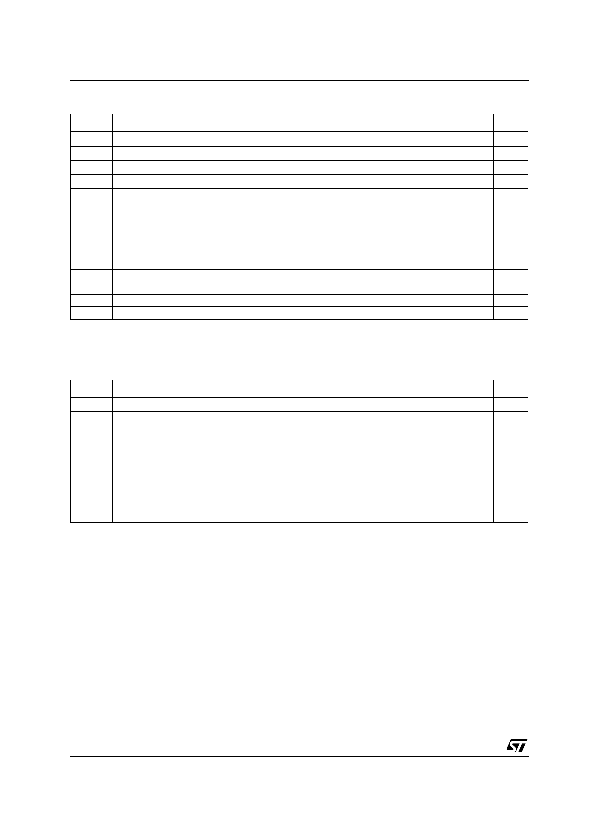
Fig. 1 : Open Loop Frequency Response
0
60
40
Phase
20
Gain (dB)
0
-20
-40
0.3 1 10 100 1000 10000
Gain
Frequency (kHz)
Vcc = 5V
RL = 8
Tamb = 25°C
Ω
-20
-40
-60
-80
-100
-120
-140
-160
-180
-200
-220
Fig. 3 : Open Loop Frequency Response
80
60
40
20
Gain (dB)
0
-20
-40
0.3 1 10 100 1000 10000
Gain
Phase
Frequency (kHz)
Vcc = 3.3V
RL = 8
Ω
Tamb = 25°C
0
-20
-40
-60
-80
-100
-120
-140
-160
-180
-200
-220
-240
Phase (Deg)
Phase (Deg)
Fig. 2 : Open Loop Frequency Response
0
60
40
Phase
20
Gain (dB)
0
-20
-40
0.3 1 10 100 1000 10000
Gain
Frequency (kHz)
Vcc = 5V
ZL = 8Ω + 560pF
Tamb = 25°C
-20
-40
-60
-80
-100
-120
-140
-160
-180
-200
-220
Fig. 4 : Open Loop Frequency Response
Phase (Deg)
Fig. 5 : Open Loop Frequency Response
80
Phase
Gain
60
40
20
Gain (dB)
0
-20
-40
0.3 1 10 100 1000 10000
6/32
Frequency (kHz)
Vcc = 2.6V
RL = 8
Tamb = 25°C
Fig. 6 : Open Loop Frequency Response
0
-20
-40
Ω
-60
-80
-100
-120
-140
-160
Phase (Deg)
-180
-200
-220
-240
80
Vcc = 2.6V
ZL = 8Ω + 560pF
Tamb = 25°C
60
40
20
Gain (dB)
0
-20
-40
0.3 1 10 100 1000 10000
Gain
Phase
Frequency (kHz)
0
-20
-40
-60
-80
-100
-120
-140
-160
-180
-200
-220
-240
Phase (Deg)

TS4890
0.3 1 10 100 1000 10000
-40
-20
0
20
40
60
80
100
-240
-220
-200
-180
-160
-140
-120
-100
-80
Gain (dB)
Frequency (kHz)
Vcc = 3.3V
CL = 560pF
Tamb = 25°C
Gain
Phase
Phase (Deg)
0.3 1 10 100 1000 10000
-40
-20
0
20
40
60
80
100
-240
-220
-200
-180
-160
-140
-120
-100
-80
Gain (dB)
Frequency (kHz)
Vcc = 2.2V
CL = 560pF
Tamb = 25°C
Gain
Phase
Phase (Deg)
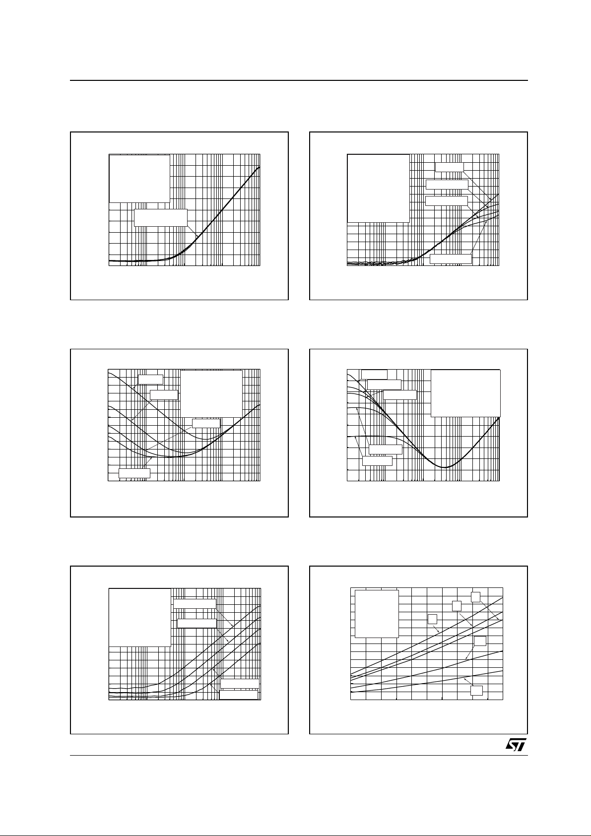
Fig. 7 : Open Loop Frequency Response
80
Phase
Gain
Frequency (kHz)
60
40
20
Gain (dB)
0
-20
-40
0.3 1 10 100 1000 10000
Vcc = 2.2V
RL = 8
Tamb = 25°C
0
-20
Ω
-40
-60
-80
-100
-120
-140
-160
-180
-200
-220
-240
Fig. 9 : Open Loop Frequency Response
100
80
60
Gain
40
20
Gain (dB)
0
Vcc = 5V
CL = 560pF
-20
Tamb = 25°C
-40
0.3 1 10 100 1000 10000
Phase
Frequency (kHz)
-80
-100
-120
-140
-160
-180
-200
-220
Phase (Deg)
Phase (Deg)
Fig. 8 : Open Loop Frequency Response
80
Vcc = 2.2V
RL = 8Ω, + 560pF
Tamb = 25°C
60
40
20
Gain (dB)
0
-20
-40
0.3 1 10 100 1000 10000
Gain
Phase
Frequency (kHz)
0
-20
-40
-60
-80
-100
-120
-140
-160
-180
-200
-220
-240
Fig. 10 : Open Loop Frequency Response
Phase (Deg)
Fig. 11 : Open Loop Frequency Response
100
80
60
Gain
40
20
Gain (dB)
0
Vcc = 2.6V
-20
CL = 560pF
Tamb = 25°C
-40
0.3 1 10 100 1000 10000
Phase
Frequency (kHz)
-80
-100
-120
-140
-160
-180
-200
-220
-240
Fig. 12 : Open Loop Frequency Response
Phase (Deg)
7/32
TS4890
10 100 1000 10000 100000
-80
-70
-60
-50
-40
-30
-20
-10
Cfeed=680pF
Cfeed=330pF
Cfeed=150pF
Cfeed=0
Vcc = 5 to 2.2V
Cb = 1µF & 0.1µF
Rfeed = 22kΩ
Vripple = 200mVrms
Input = floating
RL = 8Ω
Tamb = 25°C
PSRR (dB)
Frequency (Hz)
10 100 1000 10000 100000
-60
-50
-40
-30
-20
-10
Cin=22nF
Cin=100nF
Cin=220nF
Cin=330nF
Cin=1µF
Vcc = 5 to 2.2V
Rfeed = 22k, Rin = 22k
Cb = 1µF
Rg = 100Ω, RL = 8Ω
Tamb = 25°C
PSRR (dB)
Frequency (Hz)
Fig. 13 : Power Supply Rejection Ratio (PSRR)
vs Power supply
-30
Vripple = 200mVrms
Rfeed = 22k
-40
Input = floating
RL = 8
Tamb = 25°C
-50
PSRR (dB)
-60
-70
-80
10 100 1000 10000 100000
Ω
Ω
Vcc = 5V to 2.2V
Cb = 1µF & 0.1µF
Frequency (Hz)
Fig. 15 : Power Supply Rejection Ratio (PSRR)
vs Bypass Capacitor
-10
-20
-30
-40
-50
PSRR (dB)
-60
-70
-80
10 100 1000 10000 100000
Cb=1µF
Cb=10µF
Cb=100µF
Vcc = 5 to 2.2V
Rfeed = 22k
Rin = 22k, Cin = 1µF
Rg = 100Ω, RL = 8Ω
Tamb = 25°C
Cb=47µF
Frequency (Hz)
Fig. 14 : Power Supply Rejection Ratio (PSRR)
vs Feedback Capacitor
Fig. 16 : Power Supply Rejectio n Ratio (PSRR)
vs Input Capacitor
Fig. 17 : Power Supply Rejection Ratio (PSRR)
vs Feedback Resistor
-10
Vcc = 5 to 2.2V
-20
Cb = 1µF & 0.1µF
Vripple = 200mVrms
-30
Input = floating
RL = 8Ω
-40
Tamb = 25°C
-50
PSRR (dB)
-60
8/32
-70
-80
10 100 1000 10000 100000
Rfeed=110kΩ
Rfeed=47kΩ
Frequency (Hz)
Rfeed=22kΩ
Rfeed=10kΩ
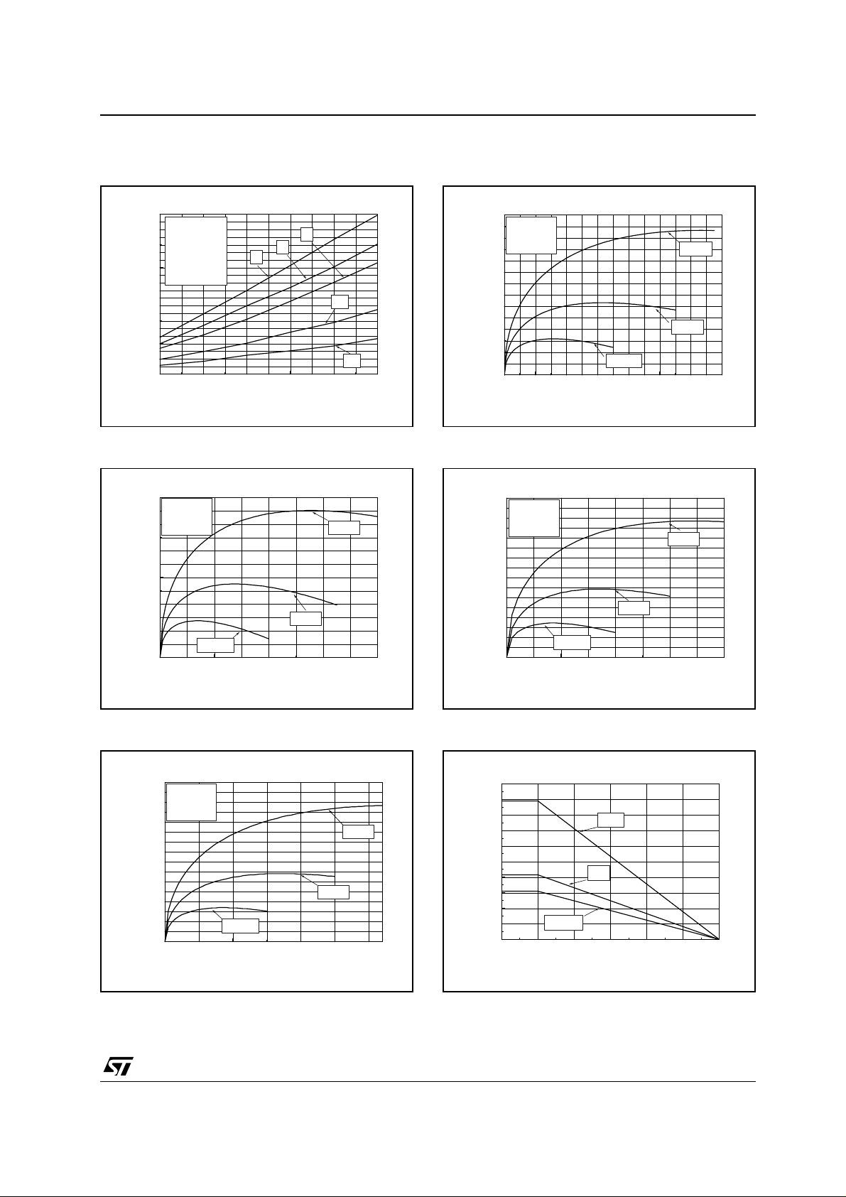
Fig. 18 : Pout @ THD + N = 1% vs Supply
Voltage vs RL
1.4
Gv = 2 & 10
1.2
Cb = 1µF
F = 1kHz
1.0
BW < 125kHz
Tamb = 25°C
0.8
0.6
0.4
0.2
Output power @ 1% THD + N (W)
0.0
2.5 3.0 3.5 4.0 4.5 5.0
Vcc (V)
4
Ω
8
Ω
6
Ω
16
Ω
32
Ω
TS4890
0.0 0.2 0.4 0.6 0.8 1.0 1.2 1.4
0.0
0.2
0.4
0.6
0.8
1.0
1.2
1.4
RL=16
Ω
RL=8
Ω
Vcc=5V
F=1kHz
THD+N<1%
RL=4
Ω
Power Dissipation (W)
Output Power (W)
0.0 0.1 0.2 0.3 0.4
0.00
0.05
0.10
0.15
0.20
0.25
0.30
0.35
0.40
RL=4
Ω
RL=8
Ω
Vcc=2.6V
F=1kHz
THD+N<1%
RL=16
Ω
Power Dissipation (W)
Output Power (W)
0 25 50 75 100 125 150
0.0
0.2
0.4
0.6
0.8
1.0
1.2
1.4
1.6
1.8
2.0
SO8
MiniSO8
QFN8
Power Dissipation (W)
Ambiant Temperature (°C)
Fig. 19 : Pout @ THD + N = 10% vs Supply
Voltage vs RL
2.0
Gv = 2 & 10
1.8
Cb = 1µF
F = 1kHz
1.6
BW < 125kHz
1.4
Tamb = 25°C
1.2
1.0
0.8
0.6
0.4
Output power @ 10% THD + N (W)
0.2
0.0
2.5 3.0 3.5 4.0 4.5 5.0
4Ω
Vcc (V)
8Ω
6Ω
16Ω
32Ω
Fig. 21 : Power Dissipation vs Pout
0.6
Vcc=3.3V
F=1kHz
0.5
THD+N<1%
0.4
RL=4
Ω
Fig. 20 : Power Dissipation vs Pout
Fig. 22 : Power Dissipation vs Pout
0.3
0.2
RL=8
Power Dissipation (W)
0.1
RL=16
0.0
0.0 0.2 0.4 0.6 0.8
Ω
Output Power (W)
Ω
Fig. 23 : Power Dissipation vs Pout
0.40
Vcc=2.6V
0.35
F=1kHz
THD+N<1%
0.30
0.25
0.20
0.15
0.10
Power Dissipation (W)
0.05
0.00
0.0 0.1 0.2 0.3
RL=16
Ω
Output Power (W)
RL=8
Ω
RL=4
Fig. 24 : Power Derating Curves
Ω
9/32
TS4890
1E-3 0.01 0.1 1
0.1
1
10
RL = 4Ω, Vcc = 3.3V
Gv = 10
Cb = Cin = 1µF
BW < 125kHz
Tamb = 25°C
20kHz
20Hz
1kHz
THD + N (%)
Output Power (W)
Fig. 25 : THD + N vs Output Power
10
Rl = 4Ω
Vcc = 5V
Gv = 2
Cb = Cin = 1µF
BW < 125kHz
Tamb = 25°C
1
THD + N (%)
0.1
1E-3 0.01 0.1 1
20kHz
20Hz, 1kHz
Output Power (W)
Fig. 27 : THD + N vs Output Power
10
RL = 4Ω, Vcc = 3.3V
Gv = 2
Cb = Cin = 1µF
BW < 125kHz
Tamb = 25°C
1
THD + N (%)
20kHz
Fig. 26 : THD + N vs Output Power
10
RL = 4Ω, Vcc = 5V
Gv = 10
Cb = Cin = 1µF
BW < 125kHz, Tamb = 25°C
1
THD + N (%)
0.1
1E-3 0.01 0.1 1
20kHz
20Hz
Output Power (W)
Fig. 28 : THD + N vs Output Power
1kHz
0.1
1E-3 0.01 0.1 1
Output Power (W)
20Hz, 1kHz
Fig. 29 : THD + N vs Output Power
10
RL = 4Ω, Vcc = 2.6V
Gv = 2
Cb = Cin = 1µF
BW < 125kHz
Tamb = 25°C
1
THD + N (%)
20kHz
20Hz, 1kHz
0.1
10/32
1E-3 0.01 0.1
Output Power (W)
Fig. 30 : THD + N vs Output Power
10
RL = 4Ω, Vcc = 2.6V
Gv = 10
Cb = Cin = 1µF
BW < 125kHz
Tamb = 25°C
1
THD + N (%)
0.1
1kHz
1E-3 0.01 0.1
20kHz
20Hz
Output Power (W)

TS4890
1E-3 0.01 0.1 1
0.1
1
10
RL = 8Ω, Vcc = 3.3V
Gv = 10
Cb = Cin = 1µF
BW < 125kHz
Tamb = 25°C
20kHz
20Hz
1kHz
THD + N (%)
Output Power (W)
Fig. 31 : THD + N vs Output Power
10
RL = 4Ω, Vcc = 2.2V
Gv = 2
Cb = Cin = 1µF
BW < 125kHz
Tamb = 25°C
1
THD + N (%)
20kHz
20Hz, 1kHz
0.1
1E-3 0.01 0.1
Output Power (W)
Fig. 33 : THD + N vs Output Power
10
RL = 8Ω
Vcc = 5V
Gv = 2
Cb = Cin = 1µF
BW < 125kHz
Tamb = 25°C
1
THD + N (%)
20Hz, 1kHz
20kHz
Fig. 32 : THD + N vs Output Power
10
RL = 4Ω, Vcc = 2.2V
Gv = 10
Cb = Cin = 1µF
BW < 125kHz
Tamb = 25°C
1
THD + N (%)
0.1
1kHz
1E-3 0.01 0.1
20kHz
20Hz
Output Power (W)
Fig. 34 : THD + N vs Output Power
10
RL = 8Ω
Vcc = 5V
Gv = 10
Cb = Cin = 1µF
BW < 125kHz
Tamb = 25°C
1
THD + N (%)
20kHz20Hz
0.1
1E-3 0.01 0.1 1
Output Power (W)
Fig. 35 : THD + N vs Output Power
10
RL = 8Ω, Vcc = 3.3V
Gv = 2
Cb = Cin = 1µF
BW < 125kHz
Tamb = 25°C
1
THD + N (%)
20Hz, 1kHz
0.1
1E-3 0.01 0.1 1
20kHz
Output Power (W)
0.1
1kHz
1E-3 0.01 0.1 1
Output Power (W)
Fig. 36 : THD + N vs Output Power
11/32

TS4890
Fig. 37 : THD + N vs Output Power
10
RL = 8Ω, Vcc = 2.6V
Gv = 2
Cb = Cin = 1µF
BW < 125kHz
Tamb = 25°C
1
THD + N (%)
20Hz, 1kHz
0.1
1E-3 0.01 0.1
20kHz
Output Power (W)
Fig. 39 : THD + N vs Output Power
10
RL = 8Ω, Vcc = 2.2V
Gv = 2
Cb = Cin = 1µF
BW < 125kHz
Tamb = 25°C
1
Fig. 38 : THD + N vs Output Power
10
RL = 8Ω, Vcc = 2.6V
Gv = 10
Cb = Cin = 1µF
BW < 125kHz
Tamb = 25°C
1
THD + N (%)
0.1
1E-3 0.01 0.1
20Hz
Output Power (W)
20kHz
1kHz
Fig. 40 : THD + N vs Output Power
10
RL = 8Ω, Vcc = 2.2V
Gv = 10
Cb = Cin = 1µF
BW < 125kHz
Tamb = 25°C
1
THD + N (%)
1kHz
0.1
1E-3 0.01 0.1
20Hz
Output Power (W)
20kHz
Fig. 41 : THD + N vs Out p ut Po wer
10
RL = 8Ω
Vcc = 5V
Gv = 2
Cb = 0.1µF, Cin = 1µF
BW < 125kHz
Tamb = 25°C
1
20kHz
THD + N (%)
0.1
1E-3 0.01 0.1 1
Output Power (W)
1kHz
20Hz
THD + N (%)
0.1
1E-3 0.01 0.1
20Hz
Output Power (W)
20kHz
1kHz
Fig. 42 : THD + N vs Outp ut Po wer
10
RL = 8Ω, Vcc = 5V, Gv = 10
Cb = 0.1µF, Cin = 1µF
BW < 125kHz, Tamb = 25°C
1
THD + N (%)
0.1
1E-3 0.01 0.1 1
20kHz
Output Power (W)
20Hz
1kHz
12/32

TS4890
1E-3 0.01 0.1 1
0.1
1
10
RL = 8Ω, Vcc = 3.3V, Gv = 10
Cb = 0.1µF, Cin = 1µF
BW < 125kHz, Tamb = 25°C
20kHz
20Hz
1kHz
THD + N (%)
Output Power (W)
Fig. 43 : THD + N vs Output Power
10
RL = 8Ω, Vcc = 3.3V
Gv = 2
Cb = 0.1µF, Cin = 1µF
BW < 125kHz
Tamb = 25°C
1
20Hz
THD + N (%)
0.1
1E-3 0.01 0.1 1
20kHz
1kHz
Output Power (W)
Fig. 45 : THD + N vs Output Power
10
RL = 8Ω, Vcc = 2.6V
Gv = 2
Cb = 0.1µF, Cin = 1µF
BW < 125kHz
Tamb = 25°C
1
THD + N (%)
0.1
20Hz
20kHz
1kHz
Fig. 44 : THD + N vs Output Power
Fig. 46 : THD + N vs Output Power
10
RL = 8Ω, Vcc = 2.6V, Gv = 10
Cb = 0.1µF, Cin = 1µF
BW < 125kHz, Tamb = 25°C
1
20Hz
0.1
THD + N (%)
20kHz
1kHz
Fig. 47 : THD + N vs Output Power
1E-3 0.01 0.1
10
RL = 8Ω, Vcc = 2.2V
Gv = 2
Cb = Cin = 1µF
BW < 125kHz
Tamb = 25°C
1
THD + N (%)
0.1
1E-3 0.01 0.1
20Hz
Output Power (W)
20kHz
1kHz
Output Power (W)
1E-3 0.01 0.1
Output Power (W)
Fig. 48 : THD + N vs Output Power
10
RL = 8Ω, Vcc = 2.2V, Gv = 10
Cb = 0.1µF, Cin = 1µF
BW < 125kHz, Tamb = 25°C
1
THD + N (%)
0.1
1E-3 0.01 0.1
20kHz
1kHz
Output Power (W)
20Hz
13/32

TS4890
1E-3 0.01 0.1
0.01
0.1
1
10
RL = 16
Ω
Vcc = 3.3V
Gv = 10
Cb = Cin = 1µF
BW < 125kHz
Tamb = 25°C
20kHz
20Hz
1kHz
THD + N (%)
Output Power (W)
1E-3 0.01 0.1
0.01
0.1
1
10
RL = 16
Ω
Vcc = 2.6V
Gv = 10
Cb = Cin = 1µF
BW < 125kHz
Tamb = 25°C
20kHz
20Hz
1kHz
THD + N (%)
Output Power (W)
Fig. 49 : THD + N vs Output Power
10
RL = 16Ω, Vcc = 5V
Gv = 2
Cb = Cin = 1µF
BW < 125kHz
1
Tamb = 25°C
THD + N (%)
0.1
0.01
1E-3 0.01 0.1 1
20kHz
20Hz, 1kHz
Output Power (W)
Fig. 51 : THD + N vs Output Power
10
RL = 16Ω, Vcc = 3.3V
Gv = 2
Cb = Cin = 1µF
BW < 125kHz
1
Tamb = 25°C
Fig. 50 : THD + N vs Output Power
10
RL = 16Ω, Vcc = 5V
Gv = 10
Cb = Cin = 1µF
BW < 125kHz
1
Tamb = 25°C
20kHz
THD + N (%)
0.1
1kHz
0.01
1E-3 0.01 0.1 1
20Hz
Output Power (W)
Fig. 52 : THD + N vs Output Power
THD + N (%)
0.1
0.01
1E-3 0.01 0.1
20kHz
20Hz, 1kHz
Output Power (W)
Fig. 53 : THD + N vs Output Power
10
RL = 16
Ω
Vcc = 2.6V
Gv = 2
Cb = Cin = 1µF
1
BW < 125kHz
Tamb = 25°C
THD + N (%)
0.1
0.01
1E-3 0.01 0.1
20kHz
20Hz, 1kHz
Output Power (W)
Fig. 54 : THD + N vs Output Power
14/32

TS4890
1E-3 0.01 0.1
0.01
0.1
1
10
RL = 16Ω Vcc = 2.2V
Gv = 10, Cb = Cin = 1µF
BW < 125kHz, Tamb = 25°C
20kHz
20Hz
1kHz
THD + N (%)
Output Power (W)
20 100 1000 10000
0.01
0.1
1
Pout = 600mW
Pout = 1.2W
RL = 4Ω, Vcc = 5V
Gv = 10
Cb = 1µF
BW < 125kHz
Tamb = 25°C
THD + N (%)
Frequency (Hz)
Fig. 55 : THD + N vs Output Power
10
RL = 16
Ω
Vcc = 2.2V
Gv = 2
Cb = Cin = 1µF
1
BW < 125kHz
Tamb = 25°C
THD + N (%)
0.1
0.01
1E-3 0.01 0.1
20Hz
20kHz
1kHz
Output Power (W)
Fig. 57 : THD + N vs Frequency
RL = 4Ω, Vcc = 5V
Gv = 2
Cb = 1µF
1
BW < 125kHz
Tamb = 25°C
Pout = 1.2W
Fig. 56 : THD + N vs Output Power
Fig. 58 : THD + N vs Frequency
THD + N (%)
Pout = 600mW
0.1
20 100 1000 10000
Frequency (Hz)
Fig. 59 : THD + N vs Frequency
RL = 4Ω, Vcc = 3.3V
Gv = 2
Cb = 1µF
1
BW < 125kHz
Tamb = 25°C
Pout = 540mW
THD + N (%)
Pout = 270mW
0.1
20 100 1000 10000
Frequency (Hz)
Fig. 60 : THD + N vs Frequency
RL = 4Ω, Vcc = 3.3V
Gv = 10
Cb = 1µF
BW < 125kHz
1
Tamb = 25°C
Pout = 540mW
THD + N (%)
0.1
20 100 1000 10000
Pout = 270mW
Frequency (Hz)
15/32

TS4890
20 100 1000 10000
0.1
1
Pout = 240 & 120mW
RL = 4Ω, Vcc = 2.6V
Gv = 10
Cb = 1µF
BW < 125kHz
Tamb = 25°C
THD + N (%)
Frequency (Hz)
Fig. 61 : THD + N vs Frequency
RL = 4Ω, Vcc = 2.6V
Gv = 2
Cb = 1µF
1
BW < 125kHz
Tamb = 25°C
Pout = 240mW
THD + N (%)
Pout = 120mW
0.1
20 100 1000 10000
Frequency (Hz)
Fig. 63 : THD + N vs Frequency
RL = 4Ω, Vcc = 2.2V
Gv = 2
Cb = 1µF
1
BW < 125kHz
Tamb = 25°C
Pout = 175mW
THD + N (%)
Fig. 62 : THD + N vs Frequency
Fig. 64 : THD + N vs Frequency
RL = 4Ω, Vcc = 2.2V
Gv = 10
1
Cb = 1µF
BW < 125kHz
Tamb = 25°C
THD + N (%)
Pout = 175mW
Pout = 88mW
Pout = 88mW
0.1
20 100 1000 10000
Fig. 65 : THD + N vs Frequency
1
THD + N (%)
0.1
20 100 1000 10000
Frequency (Hz)
Cb = 0.1µF
Cb = 1µF
Frequency (Hz)
RL = 8
Ω
Vcc = 5V
Gv = 2
Pout = 900mW
BW < 125kHz
Tamb = 25°C
Fig. 66 : THD + N vs Frequency
0.1
20 100 1000 10000
1
THD + N (%)
0.1
20 100 1000 10000
Frequency (Hz)
Cb = 0.1µF
Cb = 1µF
Frequency (Hz)
RL = 8
Vcc = 5V
Gv = 2
Pout = 450mW
BW < 125kHz
Tamb = 25°C
Ω
16/32

TS4890
20 100 1000 10000
0.1
1
Cb = 0.1µF
Cb = 1µF
RL = 8Ω, Vcc = 3.3V
Gv = 10
Pout = 200mW
BW < 125kHz
Tamb = 25°C
THD + N (%)
Frequency (Hz)
Fig. 67 : THD + N vs Frequency
RL = 8Ω, Vcc = 5V
Gv = 10
Pout = 900mW
1
Cb = 0.1µF
THD + N (%)
Cb = 1µF
0.1
20 100 1000 10000
Frequency (Hz)
BW < 125kHz
Tamb = 25°C
Fig. 69 : THD + N vs Frequency
1
Cb = 0.1µF
RL = 8Ω, Vcc = 3.3V
Gv = 2
Pout = 400mW
BW < 125kHz
Tamb = 25°C
Fig. 68 : THD + N vs Frequency
RL = 8Ω, Vcc = 5V
Gv = 10
Pout = 450mW
1
Cb = 0.1µF
THD + N (%)
0.1
Cb = 1µF
20 100 1000 10000
Frequency (Hz)
BW < 125kHz
Tamb = 25°C
Fig. 70 : THD + N vs Frequency
1
Cb = 0.1µF
RL = 8Ω, Vcc = 3.3V
Gv = 2
Pout = 200mW
BW < 125kHz
Tamb = 25°C
THD + N (%)
0.1
20 100 1000 10000
Cb = 1µF
Frequency (Hz)
Fig. 71 : THD + N vs Frequency
RL = 8Ω, Vcc = 3.3V
Gv = 10
1
Cb = 0.1µF
THD + N (%)
0.1
Cb = 1µF
20 100 1000 10000
Frequency (Hz)
Pout = 400mW
BW < 125kHz
Tamb = 25°C
THD + N (%)
0.1
20 100 1000 10000
Cb = 1µF
Frequency (Hz)
Fig. 72 : THD + N vs Frequency
17/32

TS4890
20 100 1000 10000
0.1
1
Cb = 0.1µF
Cb = 1µF
RL = 8Ω, Vcc = 2.6V
Gv = 10
Pout = 110mW
BW < 125kHz
Tamb = 25°C
THD + N (%)
Frequency (Hz)
Fig. 73 : THD + N vs Frequency
1
Cb = 0.1µF
Cb = 1µF
THD + N (%)
0.1
20 100 1000 10000
Frequency (Hz)
RL = 8Ω, Vcc = 2.6V
Gv = 2
Pout = 220mW
BW < 125kHz
Tamb = 25°C
Fig. 75 : THD + N vs Frequency
RL = 8Ω, Vcc = 2.6V
Gv = 10
Pout = 220mW
1
Cb = 0.1µF
BW < 125kHz
Tamb = 25°C
Fig. 74 : THD + N vs Frequency
1
Cb = 0.1µF
THD + N (%)
0.1
20 100 1000 10000
Cb = 1µF
Frequency (Hz)
RL = 8Ω, Vcc = 2.6V
Gv = 2
Pout = 110mW
BW < 125kHz
Tamb = 25°C
Fig. 76 : THD + N vs Frequency
THD + N (%)
0.1
Cb = 1µF
20 100 1000 10000
Frequency (Hz)
Fig. 77 : THD + N vs Frequency
1
Cb = 0.1µF
Cb = 1µF
THD + N (%)
0.1
20 100 1000 10000
Frequency (Hz)
RL = 8Ω, Vcc = 2.2V
Gv = 2
Pout = 150mW
BW < 125kHz
Tamb = 25°C
Fig. 78 : THD + N vs Frequency
1
Cb = 0.1µF
THD + N (%)
0.1
20 100 1000 10000
Cb = 1µF
Frequency (Hz)
RL = 8Ω, Vcc = 2.2V
Gv = 2
Pout = 75mW
BW < 125kHz
Tamb = 25°C
18/32

TS4890
20 100 1000 10000
0.01
0.1
1
Pout = 310mW
Pout = 620mW
RL = 16Ω, Vcc = 5V
Gv = 10, Cb = 1µF
BW < 125kHz
Tamb = 25°C
THD + N (%)
Frequency (Hz)
20 100 1000 10000
0.1
1
Pout = 135mW
Pout = 270mW
RL = 16Ω, Vcc = 3.3V
Gv = 10
Cb = 1µF
BW < 125kHz
Tamb = 25°C
THD + N (%)
Frequency (Hz)
Fig. 79 : THD + N vs Frequency
RL = 8Ω, Vcc = 2.2V
Gv = 10
Pout = 150mW
1
Cb = 0.1µF
THD + N (%)
Cb = 1µF
0.1
20 100 1000 10000
Frequency (Hz)
BW < 125kHz
Tamb = 25°C
Fig. 81 : THD + N vs Frequency
1
Pout = 310mW
0.1
THD + N (%)
Pout = 620mW
RL = 16Ω, Vcc = 5V
Gv = 2, Cb = 1µF
BW < 125kHz
Tamb = 25°C
Fig. 80 : THD + N vs Frequency
RL = 8Ω, Vcc = 2.2V
Gv = 10
1
Cb = 0.1µF
Cb = 1µF
THD + N (%)
0.1
20 100 1000 10000
Frequency (Hz)
Pout = 72mW
BW < 125kHz
Tamb = 25°C
Fig. 82 : THD + N vs Frequency
0.01
20 100 1000 10000
Frequency (Hz)
Fig. 83 : THD + N vs Frequency
1
Pout = 270mW
0.1
THD + N (%)
Pout = 135mW
0.01
20 100 1000 10000
Frequency (Hz)
RL = 16Ω, Vcc = 3.3V
Gv = 2, Cb = 1µF
BW < 125kHz
Tamb = 25°C
Fig. 84 : THD + N vs Frequency
19/32

TS4890
20 100 1000 10000
0.01
0.1
1
RL = 16Ω, Vcc = 2.2V
Gv = 10, Cb = 1µF
BW < 125kHz
Tamb = 25°C
Pout = 50mW
Pout = 100mW
THD + N (%)
Frequency (Hz)
2.5 3.0 3.5 4.0 4.5 5.0
50
60
70
80
90
RL=8
Ω
RL=4
Ω
RL=16
Ω
Gv = 10
Cb = Cin = 1µF
THD+N < 0.4%
Tamb = 25°C
2.2
SNR (dB)
Vcc (V)
Fig. 85 : THD + N vs Frequency
1
RL = 16Ω, Vcc = 2.6V
Gv = 10, Cb = 1µF
BW < 125kHz
Tamb = 25°C
0.1
THD + N (%)
0.01
20 100 1000 10000
Pout = 160mW
Pout = 80mW
Frequency (Hz)
Fig. 87 : THD + N vs Frequency
1
RL = 16Ω, Vcc = 2.2V
Gv = 2, Cb = 1µF
BW < 125kHz
Tamb = 25°C
Pout = 50 & 100mW
0.1
THD + N (%)
Fig. 86 : THD + N vs Frequency
1
RL = 16Ω, Vcc = 2.6V
Gv = 2, Cb = 1µF
BW < 125kHz
Tamb = 25°C
0.1
THD + N (%)
0.01
20 100 1000 10000
Pout = 80mW
Pout = 160mW
Frequency (Hz)
Fig. 88 : THD + N vs Frequency
0.01
20 100 1000 10000
Fig. 89 : Signal to Noise Ratio vs Power Supply
with Unweighted Filter (20Hz to 20kHz)
100
90
RL=16
80
SNR (dB)
70
60
50
2.2
2.5 3.0 3.5 4.0 4.5 5.0
20/32
Ω
Frequency (Hz)
RL=8
Ω
Vcc (V)
RL=4
Ω
Gv = 2
Cb = Cin = 1µF
THD+N < 0.4%
Tamb = 25°C
Fig. 90 :Signal to Noise Ratio Vs Power Supply
with Unweighted Filter (20Hz to 20kHz)

TS4890
2.5 3.0 3.5 4.0 4.5 5.0
60
70
80
90
100
RL=8
Ω
RL=4
Ω
RL=16
Ω
Gv = 10
Cb = Cin = 1µF
THD+N < 0.4%
Tamb = 25°C
2.2
SNR (dB)
Vcc (V)
012345
0
1
2
3
4
5
6
7
Vstandby = Vcc
Tamb = 25°C
Icc (mA)
Vcc (V)
0.0 0.5 1.0 1.5 2.0 2.5 3.0
0
1
2
3
4
5
6
Vcc = 3.3V
Tamb = 25°C
Icc (mA)
Vstandby (V)
Fig. 91 : Signal to Noise Ratio vs Power Supply
with Weig h t e d Filt e r t y p e A
110
100
RL=4
Ω
Ω
Gv = 2
Cb = Cin = 1µF
THD+N < 0.4%
Tamb = 25°C
90
SNR (dB)
80
70
60
2.2
RL=16
2.5 3.0 3.5 4.0 4.5 5.0
RL=8
Ω
Vcc (V)
Fig. 93 : Frequency Response Gain vs Cin, &
Cfeed
10
5
0
-5
-10
Gain (dB)
-15
-20
-25
10 100 1000 10000
Cin = 22nF
Cin = 82nF
Cfeed = 330pF
Cin = 470nF
Frequency (Hz)
Cfeed = 680pF
Cfeed = 2.2nF
Rin = Rfeed = 22kΩ
Tamb = 25°C
Fig. 92 : Signal to Noise Ratio vs Power Supply
with Weighted Filter Type A
Fig. 94 : Current Consumption vs Power
Supply Voltage (no load)
Fig. 95 : C urrent Con sumption v s Standby
Voltage @ Vcc = 5V
7
6
5
4
3
Icc (mA)
2
1
0
0.0 0.5 1.0 1.5 2.0 2.5 3.0 3.5 4.0 4.5 5.0
Vstandby (V)
Vcc = 5V
Tamb = 25°C
Fig. 96 : C urrent Con sumption v s Standby
Voltage @ Vcc = 3.3V
21/32

TS4890
2.5 3.0 3.5 4.0 4.5 5.0
0.0
0.1
0.2
0.3
0.4
0.5
0.6
0.7
0.8
0.9
1.0
RL = 16Ω
RL = 4Ω
RL = 8Ω
Tamb = 25°C
2.2
Vout1 & Vout2
Clipping Voltage Low side (V)
Power supply Voltage (V)
Fig. 97 : C urrent Con sumption v s Standby
Voltage @ Vcc = 2.6V
6
5
4
3
Icc (mA)
2
1
0
0.0 0.5 1.0 1.5 2.0 2.5
Vstandby (V)
Vcc = 2.6V
Tamb = 25°C
Fig. 99 : Clipping Voltage vs Power Supply
Voltage and Load Resistor
1.0
Tamb = 25°C
0.9
0.8
0.7
0.6
0.5
0.4
Vout1 & Vout2
0.3
0.2
Clipping Voltage High side (V)
0.1
0.0
RL = 8Ω
2.2
2.5 3.0 3.5 4.0 4.5 5.0
Power supply Voltage (V)
RL = 4Ω
RL = 16Ω
Fig. 98 : C urrent Con sumption v s Standby
Voltage @ Vcc = 2.2V
5
4
3
Icc (mA)
2
1
0
0.0 0.5 1.0 1.5 2.0
Vstandby (V)
Vcc = 2.2V
Tamb = 25°C
Fig. 100 :Clipping Voltage vs Power Supply
Voltage and Load Resistor
Fig. 101 : Vout1+V out2 Unweighted Noise Floor
120
Vcc = 2.2V to 5V, Tamb = 25 C
Cb = Cin = 1 F
100
Input Grounded
BW = 20Hz to 20kHz (Unweighted)
80
60
40
Output Noise Voltage ( V)
20
0
22/32
20
Standby mode
100 1000 10000
Frequency (Hz)
Av = 10
Av = 2
Fig. 102 : Vout1+Vout2 A-weighted Noise Floor
120
Vcc = 2.2V to 5V, Tamb = 25 C
Cb = Cin = 1 F
100
Input Grounded
BW = 20Hz to 20kHz (A-Weighted)
80
60
40
20
Standby mode
100 1000 10000
Frequency (Hz)
Output Noise Voltage ( V)
20
0
Av = 10
Av = 2

APPLICA TI ON INFORMATION
Fig. 103 : Demoboard Schematic
TS4890
C1
R2
C2
R1
Vcc
C6
100µ
6
4
Vin-
Vin+
3
R6
Bypass
2
Standby
1
+
C8
C12
1u
Vcc
-
+
Bias
GND
7
Vcc
GND
Neg. input
P1
Pos input
P2
R7
1.5k
Vcc
S1
S2
C3
R3
C5
+
C11
R8
10k
Vcc
R4
C4 R5
S5
PositiveInput mode
S8
Standby
D1
PW ON
Fig. 104 : SO8 & MiniSO8 Demoboard Components Side
C7
+
100n
S6
OUT1
S3
GND
S4
GND
S7
Av=-1
+
Vout1
Vout2
TS4890
5
8
C9
+
470µ
C10
+
470µ
23/32

TS4890
Fig. 105 : SO8 & MiniSO8 Demoboard Top
Solder Layer
Fig. 106 :
Solder Layer
SO8 & MiniSO8 Demoboard Bottom
The output power is :
2
)Vout2(
Pout
=
RMS
R
L
)W(
For the same power supply voltage, the output
power in BTL configuration is four times higher
than the output power in single ended
configuration.
■Gain In Typical Application Schematic
(cf. page 1)
In flat region (no effect of Cin), the output voltage
of the first stage is :
Rfeed
Vin1Vout −=
Rin
For the second stage : Vout2 = -Vout1 (V)
The differential output voltage is
Vin21Vout2Vout =−
Rfeed
Rin
)V(
)V(
■BTL Configuration Principle
The TS4890 is a monolithic power amplifier with a
BTL output type. BTL (Bridge Tied Load) means
that each end of the load are connected to two
single ended output amplifiers. Thus, we have :
Single ended output 1 = Vout1 = Vout (V)
Single ended output 2 = Vout2 = -Vout (V)
And Vout1 - Vout2 = 2Vout (V)
The differential gain named gain (Gv) for more
convenient usage is :
Gv =
=
−
Vin
2
Rin
Rfeed
1Vout2Vout
Remark : Vout2 is in phase with Vin and Vout1 is
180 phased with Vin. It means that the positive
terminal of the l oudspeaker should be connected
to Vout2 and the negative to Vout1.
■Low and high frequency response
In low frequency region, the effect of Cin starts.
Cin with Rin forms a high pass filter with a -3dB cut
off frequency .
1
=
F
CL
π
RinCin2
In high frequency region, you can limit the
bandwidth by adding a capacitor (Cfeed) in
parallel on Rfeed. Its form a l ow pass filter with a
-3dB cut off frequency .
F
=
CH
1
π
(Hz)
CfeedRfeed2
)Hz(
24/32

TS4890
)V(tsinVV
PEAKOUT
ω=
)A(
R
V
I
L
OUT
OUT
=
)W(
R2
V
P
L
2
PEAK
OUT
=
)A(
R
V
2Icc
L
PEAK
AVG
π
=
)W(
R
Vcc2
maxPdiss
L
2
2
π
=
Vcc4
V
plysupP
P
PEAKOUT
π
==η
■Power dissipation and efficiency
Hypothesis :
• Voltage and current in the load are sinusoidal
(Vout and Iout)
• Supply voltage is a pure DC source (Vcc)
Regarding the load we have :
and
and
Then, the average current delivered by the supply
voltage is
The power delivered by the supply voltage is
Psupply = Vcc Icc
Then, the po wer dissip ated by the amplifier is
Pdiss = Psupply - Pout (W)
Pdiss
=
and the maximum value is obtained when
and its value is
π
AVG
R
(W)
Vcc22
L
Pdiss
∂
P
∂
OUT
−
OUTOUT
0
=
)W(PP
The maximum theoret ical value is reached when
Vpeak = V c c, so
π
%5.784=
■Decoupl i ng of the ci rc u it
Two capacitors are needed to bypass properly the
TS4890. A power supply bypass capacitor Cs and
a bias voltage bypass capacitor Cb.
Cs has especially an influence on the THD+N in
high frequency (above 7kHz) and indirectly on the
power supply disturbances.
With 100µF, you can expect similar THD+N
performances like shown in the datasheet.
If Cs is lower than 100µF, in high frequency
increase THD+N and disturbances on the power
supply rail are less fil tered.
To the contrary, if Cs is higher than 100µF, those
disturbances on the power supply rail are more
filtered.
Cb has an influence on THD+N in lower frequency,
but its function is critical on the final result of PSRR
with input grounded in lower frequency.
If Cb is lower than 1µF, THD+N increase in lower
frequency (see THD+N vs frequency curves) and
the PSRR worsens up
If Cb is higher than 1µF, the benefit on THD+N in
lower frequency is small but the ben efit on PSRR
is substantial (see PSRR vs. Cb curves).
Note that Cin has a non-negligible effect on PSRR
in lower frequency. Lower is its value, higher is the
PSRR (see fig. 13).
■Pop and Click performance
In order to have the best performances with the
pop and click circuitry, the formula below must be
follow :
τ≤τ
bin
Remark : This maximum valu e is only depending
on power supply voltage and load values.
The efficiency is the ratio between the output
power and the power supply
With
and
×+=τ
)s(C)RR(
infeedinin
)s(Ck50bb×Ω=τ
25/32

TS4890
)W(
R
Vcc2
maxPdiss
L
2
2
π
=
nF795
FRin2
1
C
CL
IN
=
π
=
■Power amplifier design examples
Given :
• Load impedance : 8Ω
• Output power @ 1% THD+N : 0.5W
• Input impedance : 10kΩ min.
• Input voltage peak to peak : 1Vpp
• Bandwidth frequency : 20Hz to 20kHz (0, -3dB)
• THD+N in 20Hz to 20kHz < 0.5% @Pout=0.45W
• Ambient temperature max = 50°C
• SO8 package
First of all, we must cal culate t he m inimum p ower
supply voltage to obtain 0.5W into 8Ω. See curves
in fig. 15, we can read 3.5V. Thus, the power
supply voltage value min. will be 3.5V.
Following the maximum power dissipation
equation :
with 3.5V we have Pdissmax=0.31W.
Refer to power derating curves (fig. 24), with
0.31W the maxim um ambien t temperature will be
100°C. This last value could be higher if you follow
the example layout shows on the demoboard
(better dissipation).
The gain of the amplifier in flat region will be :
The first amplifier has a gain of
Rfeed
Rin
3
=
and the theoretical val ue of t he -3dB cut of hig her
frequency is 2MHz/3 = 660kHz.
We can keep this value or limiting the bandwidth
by adding a capacitor Cfeed, in paralle l on Rfeed.
Then
C
FEED
=
1
π
FR2
CHFEED
pF265
=
So, we could use for Cfeed a 220pF capacitor
value that gives 24kHz.
Now, we can choose the value of Cb with the
constraint THD+N in 20Hz to 20kHz < 0.5% @
Pout=0.45W. If you refer to the closest THD+N vs
frequency measurement : fig. 71 (Vcc=3.3V,
Gv=10), with Cb = 1µF, the THD+N vs frequency
is always below 0.4%. As the behaviour is the
same with Vcc = 5V (fig. 67), V cc = 2.6V (fig. 67).
As the gain for these measurements is higher
(worst case), we can consider with Cb = 1µF, Vcc
= 3.5V and G v = 6, that the THD+N in 20Hz to
20kHz range with Pout = 0.45W will be lower than
0.4%.
In the following tables, you could find three
another examples with values required for the
demoboard.
V
INPP
PR22
OUTL
65.5
===
V
G
OUTPP
V
V
INPP
We have Rin > 10kΩ. Let's take Rin = 10kΩ, then
Rfeed = 28.25kΩ. We could use for Rfeed = 30kΩ
in normalized value and the gain w ill be Gv = 6.
In lower frequency we want 20 Hz (-3dB cut off
frequency). Then
So, we could use for Cin a 1µF capacitor value that
gives 16Hz.
In Higher frequency we want 20k Hz (-3dB cut off
frequency). The Gain Bandwidth Product of the
TS4890 is 2MHz typical and doesn't change when
the amplifier delivers power into the load.
26/32
Remark : components with (*) marking are
optional.
Application n°1 : 20Hz to 20kHz bandwidth and
6dB gain BTL power amplifier.
Components :
Designator Part Type
R1 22k / 0.125W
R4 22k / 0.125W
R6 Short Cicuit
R7* (Vcc-Vf_led)/If_led
R8 10k / 0.125W
C5 470nF
C6 100µF

TS4890
Designator Part Type
C7 100nF
C9 Short Circuit
C10 Short Circuit
C12 1µF
S1, S2, S6, S7
S8
P1 PCB Phono Jack
D1* Led 3mm
U1 TS4890ID or TS4890IS
2mm insulated Plug
10.16mm pitch
3 pts connector 2.54mm
pitch
Application n°2 : 20Hz to 20kHz bandwidth and
20dB gai n BTL power am pl i fie r.
Components :
Designator Part Type
R1 110k / 0.125W
R4 22k / 0.125W
R6 Short Cicuit
R7* (Vcc-Vf_led)/If_led
R8 10k / 0.125W
C5 470nF
C6 100µF
C7 100nF
Application n°3 : 50Hz to 10kHz bandwidth and
10dB gai n BTL power am pl i fie r.
Components :
Designator Part Type
R1 33k / 0.125W
R2 Short Circuit
R4 22k / 0.125W
R6 Short Cicuit
R7* (Vcc-Vf_led)/If_led
R8 10k / 0.125W
C2 470pF
C5 150nF
C6 100µF
C7 100nF
C9 Short Circuit
C10 Short Circuit
C12 1µF
S1, S2, S6, S7
S8
P1 PCB Phono Jack
D1* Led 3mm
U1 TS4890ID or TS4890IS
2mm insulated Plug
10.16mm pitch
3 pts connector 2.54mm
pitch
C9 Short Circuit
C10 Short Circuit
C12 1µF
S1, S2, S6, S7
S8
P1 PCB Phono Jack
D1* Led 3mm
U1 TS4890ID or TS4890IS
2mm insulated Plug
10.16mm pitch
3 pts connector 2.54mm
pitch
Application n°4 : Differential inputs BTL power
amplifier.
In this configuration, we need to place these
components : R1, R4, R5, R6, R7, C4, C5, C12.
We have also : R4 = R5, R1 = R6, C4 = C5.
The gain of the amplifier is:
GVDIFF = 2
R1
------- R4
For Vcc=5V, a 20Hz to 20kHz bandwidth and 20dB
gain BTL power amplifier you could follow the bill
of material below.
27/32

TS4890
Components :
Designator Part Type
R1 110k / 0.125W
R4 22k / 0.125W
R5 22k / 0.125W
R6 110k / 0.125W
R7* (Vcc-Vf_led)/If_led
R8 10k / 0.125W
C4 470nF
C5 470nF
C6 100µF
C7 100nF
C9 Short Circuit
C10 Short Circuit
C12 1µF
D1* Led 3mm
S1, S2, S6, S7
S8
P1, P2 PCB Phono Jack
U1 TS4890ID or TS4890IS
2mm insulated Plug
10.16mm pitch
3 pts connector 2.54mm
pitch
28/32

TS4890
■Note on how to use the PSRR curves
(page 8)
We have finished a design and we have chosen for
the components :
• Rin=Rfeed=22kΩ
• Cin=100nF
• Cb=1µF
Now, on fig. 16, we can see the PSRR (input
grounded) vs frequency curves. At 217Hz, we
have a PSRR value of -36dB.
In reality we want a value about -70dB. So, we
need a gain of 34dB !
Now, on fig. 15 we can see the effect of Cb on the
PSRR (input grounded) vs. frequency. With
Cb=100µF, we can reach the -70dB value.
The process to obtain the final curve (Cb=100µF,
Cin=100nF, Rin=Rfeed=22kΩ) is a simple transfer
point by point on each frequency of the curve on
fig. 16 to the curve on fig. 15.
The measurement result is shown on the next
figure.
Fig. 107 : PSRR changes with Cb
-30
Cin=100nF
-40
Cb=1µF
-50
PSRR (dB)
-60
Cin=100nF
Cb=100µF
Vcc = 5 & 2.2V
Rfeed = 22k, Rin = 22k
Rg = 100Ω, RL = 8
Tamb = 25°C
Ω
How do we measure the PSRR ?
Fig. 108 : PSRR measurement schematic
Rfeed
Vripple
Vcc
Rin
Cin
Rg
100 Ohms
4
Vin-
Vin+
3
Bypass
2
Standby
1
Cb
6
Vcc
-
+
Av=-1
+
Bias
GND
7
Vout1
Vout2
TS4890
5
Vs-
RL
8
Vs+
■Principle of operation
• We fixed the DC voltage supply (Vcc)
• We fixed the AC sinusoidal ripple voltage
(Vripple)
• No bypass capacitor Cs is used
The PSRR value for each frequency is :
)V(Rms
×=
Log20)dB(PSRR
10
ripple
Remark : The measure of the Rms voltage is not a
Rms selective measure but a full range (2 Hz to
125 kHz) Rms measure. It means that we
measure the effective Rms signal + the noise.
−
)VsVs(Rms
−+
-70
10 100 1000 10000 100000
Frequency (Hz)
■Note on PSRR measurement
What is the PSRR ?
The PSRR is the Power Suppl y Rejection Ratio.
It's a kind of SVR in a determined frequency range.
The PSRR of a device, is the ratio between a
power supply disturbance and the result on the
output. We can say that the PSRR is the ability of
a device to m inimize the impact o f power supply
disturbances to the output.
29/32

TS4890
PACKAGE MECHANICAL DATA
SO-8 MECHANICAL DATA
DIM.
A 1.35 1.75 0.053 0.069
A1 0.10 0.25 0.04 0.010
A2 1.10 1.65 0.043 0.065
B 0.33 0.51 0.013 0.020
C 0.19 0.25 0.007 0.010
D 4.80 5.00 0.189 0.197
E 3.80 4.00 0.150 0.157
e 1.27 0.050
H 5.80 6.20 0.228 0.244
h 0.25 0.50 0.010 0.020
L 0.40 1.27 0.016 0.050
k ˚ (max.)
ddd 0.1 0.04
MIN. TYP MAX. MIN. TYP. MAX.
mm. inch
8
30/32
0016023/C

PACKAGE MECHANICAL DATA
TS4890
31/32

TS4890
e
m
s
n
r
PACKAGE MECHANICAL DATA
Information furnished is believed to b e accurate and reliable. However, STMicroelectroni cs assumes no responsibility for th
consequences of use of such information nor for any infringement of patents or other rights of third parties which may result fro
its use. No license is granted by implication or otherwise under any pat ent or patent rights of S TMi croele ctronics. S pecification
mentioned in this publication are subj ect to change without notice. This publication supe rsedes and replaces all informatio
previously supplied. STMicroelectro nics products are not authorize d for use as critical compon ents in life support dev ices o
systems without express written approval of STMicroelectronics.
Australi a - Brazil - China - Finlan d - F rance - Germ any - Hong Kong - India - It al y - Japan - Ma l aysia - Malta - Morocco
32/32
The ST logo is a registered trademark of STMicroelectronics
© 2003 STM icroelectr o n i cs - All Rig h ts Reserve d
STMicroelectronics GROUP OF COMPANIES
Singap ore - Spain - Sweden - Switzerland - United Kingdom
 Loading...