


s
TS4872
RAIL TO RAIL INPU T/OU TPUT
1W AUDIO POWER AMPLIFIER WITH STANDBY MODE
■OPERATING FROM V
= 2.2V to 5.5V
CC
■RAIL TO RAIL INPUT/OUTPUT
■1W OUTPUT POWER @ Vcc=5V, THD=1%,
f=1kHz, with 8
Ω Load
■ULTRA LOW CONSUMPTION IN STANDBY
MODE (10nA)
■75dB PSRR @ 217Hz @ 5 & 2.6V
■ULTRA LOW POP & CLICK
■ULTRA LOW DISTORTION (0.05%)
■UNITY GAIN STABLE
■8 X170µm BUMPS FLIP CHIP PACKAGE
DESCRIPTION
The TS487 2 i s an Audio Pow er Amplifier capable
of delivering 1W of continuous RMS Ouput Power
into 8
Ω load @ 5V.
This Audio Am plifier is exhibiting 0.1% distortion
level (THD) from a 5V supply for a Pout = 250mW
RMS. An external standby mode cont rol reduces
the supply current to less than 10n A. An internal
shutdown protection is provided.
PIN CONNECTIONS (Top View)
TS4872IJT - FLIP CHIP
8
Vout1
76
+
Vin
Vin
12
Vcc
GND
5
STDBY
Vout2
BYPASS
3
4
The TS4872 has been designed for high quality
audio applications such as m obile phones and t o
minimize the number of external components.
The unity-gain stable amplifier can be configured
by external gain setting resistors.
APPLICATIONS
■Mobile Phones (Cellular / Cordless)
■PDAs
■Laptop/Notebook computers
■Portable Audio Devices
ORDER CODE
Part
Number
Temperature
Range
TS4872IJT -40, +85°C ● YW4872
J = Flip Chip Package - only available in Tape & Reel (JT)
October 2002
Package
Marking
J
TYPICAL APPLICATION SCHEMATIC
Cfeed
Vcc
Rfeed
6
Audio
Input
Vcc
Rstb
Rin
1
Vin-
Cin
Vin+
7
Bypass
3
Standby
5
Cb
Vcc
-
+
Bias
GND
2
Av=-1
+
Vout1
Vout2
TS4872
Cs
8
RL
8 Ohm
4
1/29

TS4872
ABSOLUTE MAXIMUM RATINGS
Symbol Parameter Value Unit
V
T
T
R
Supply voltage
CC
V
Input Voltage
i
Operating Free Air Temperature Range -40 to + 85 °C
oper
Storage Temperature -65 to +150 °C
stg
T
Maximum Junction Temperature 150 °C
j
Flip Chip Thermal Resistance Junction to Ambient
thja
Pd Power Dissipation Internally Limited
ESD Human Body Model 2 kV
ESD Machine Model 200 V
Latch-up Latch-up Immunity Class A
Lead Te mpera ture (solde ring, 10sec ) 250 °C
1. All voltages values are measured with respect to the ground pin.
2. The magnitude of input signal must never exceed V
3. Device is protected in cas e of over temperature by a thermal shutdown active @ 150°C
OPERATING CONDITIONS
Symbol Parameter Value Unit
V
V
V
R
1. With Heat Sink Surface = 125mm
Supply Voltage 2.2 to 5.5 V
CC
Common Mode Input Voltage Range
ICM
V
V
Standby Voltage Input :
STB
Device ON
Device OFF
RL
Load Resistor 4 - 32
Flip Chip Thermal Resistance Junction to Ambient
thja
1)
2)
from 2.6V to 5V
CC
< 2.6V
CC
2
+ 0.3V / GND - 0.3V
CC
6V
GND to V
3)
G
CC
200 °C/W
to V
ND
CC
VCC / 2
V
≤
G
ND
V
- 0.5V ≤ V
CC
1)
≤ 0.5V
STB
≤ V
STB
CC
95 °C/W
V
V
Ω
2/29

TS4872
ELECTRICAL CHARACTERISTICS
V
= +5V, GND = 0V , T
CC
Symbol Parameter Min. Typ. Max. Unit
= 25°C (unless otherwise specified)
amb
I
I
STANDBY
Voo
Po
THD + N
PSRR
Φ
GM
GBP
1. Standby mode i s actived when Vstdby is tied to Vcc
2. Dynamic measurements - 20*log(r m s(Vout)/rms(Vripple)). Vripple is the surim posed sinus signal to Vc c @ f = 217Hz
V
= +3.3V, GND = 0V, T
CC
Supply Current
CC
No input signal, no load
Standby Current
No input signal, Vstdby = Vcc, RL = 8
Output Offset Voltage
No input signal, RL = 8
Output Power
THD = 1% Max, f = 1kHz, RL = 8
Total Harmonic Distortion + Noise
Po = 250mW rms, Gv = 2, 20Hz < f < 20kHz, RL = 8
Power Supply Rejection Ratio
f = 217Hz, RL = 8
Phase Margin at Unity Gain
M
R
= 8Ω, CL = 500pF
L
Gain Margin
R
= 8Ω, CL = 500pF
L
Gain Bandwidth Product
R
= 8
Ω
L
1)
Ω
Ω
Ω
2)
RFeed = 22K
Ω,
= 25°C (unless otherwise specified)
amb
Vripple = 200mV rms
Ω,
68mA
10 1000 nA
520mV
1W
Ω
0.1 %
75 dB
70 Degrees
20 dB
2MHz
3)
Symbol Parameter Min. Typ. Max. Unit
I
I
STANDBY
Voo
Po
THD + N
PSRR
Φ
GM
GBP
1. Standby mode i s actived when Vstdby is tied to Vcc
2. Dynamic measurements - 20*log(r m s(Vout)/rms(Vripple)). Vripple is the surim posed sinus signal to Vc c @ f = 217Hz
All electrical values are made by correlatio n bet ween 2.6v and 5v measurem ents
3
Supply Current
CC
No input signal, no load
Standby Current
No input signal, Vstdby = Vcc, RL = 8
Output Offset Voltage
No input signal, RL = 8
Output Power
THD = 1% Max, f = 1kHz, RL = 8
Total Harmonic Distortion + Noise
Po = 250mW rms, Gv = 2, 20Hz < f < 20kHz, RL = 8
Power Supply Rejection Ratio
f = 217Hz, RL = 8
Phase Margin at Unity Gain
M
R
= 8Ω, CL = 500pF
L
Gain Margin
= 8Ω, CL = 500pF
R
L
Gain Bandwidth Product
= 8
R
Ω
L
5.5 8 mA
1)
Ω
Ω
Ω
Ω
2)
RFeed = 22KΩs, Vripple = 100mV rms
Ω,
10 1000 nA
520mV
450 mW
0.1 %
68 dB
70 Degrees
20 dB
2 MHz
3/29
TS4872
ELECTRICAL CHARACTERISTICS
V
= 2.6V, GND = 0V, T
CC
Symbol Parameter Min. Typ. Max. Unit
= 25°C (unless otherwise specified)
amb
I
CC
I
STANDBY
Voo
Po
THD + N
PSRR
Φ
GM
GBP
1. S ta ndby mode is actived when Vstdby is tied to Vcc
2. Dy namic measurements - 20*log(r m s(Vout)/rms(Vripple)). Vripple is the surim posed sinus signal to Vc c @ f = 217Hz
= 2.2V, GND = 0V, T
V
CC
Supply Current
No input signal, no load
Standby Current
1)
No input signal, Vstdby = Vcc, RL = 8
Output Offset Voltage
No input signal, RL = 8
Output Power
THD = 1% Max, f = 1kHz, RL = 8
Total Harmonic Distortion + Noise
Po = 200mW rms, Gv = 2, 20Hz < f < 20kHz, RL = 8
Power Supply Rejection Ratio
f = 217Hz, RL = 8
Phase Margin at Unity Gain
M
R
= 8Ω, CL = 500pF
L
Gain Margin
R
= 8Ω, CL = 500pF
L
Gain Bandwidth Product
R
= 8
Ω
L
amb
Ω
Ω
Ω
Ω
2)
RFeed = 22K
Ω,
Vripple = 200mV rms
Ω,
= 25°C (unless otherwise specified)
5.5 8 mA
10 1000 nA
520mV
260 mW
0.1 %
75 dB
70 Degrees
20 dB
2MHz
Symbol Parameter Min. Typ. Max. Unit
I
CC
I
STANDBY
Voo
Po
THD + N
PSRR
Φ
GM
GBP
1. S ta ndby mode is actived when Vstdby is tied to Vcc
2. Dy namic measurements - 20*log(r m s(Vout)/rms(Vripple)). Vripple is the surim posed sinus signal to Vc c @ f = 217Hz
Supply Current
No input signal, no load
Standby Current
1)
No input signal, Vstdby = Vcc, RL = 8
Output Offset Voltage
No input signal, RL = 8
Output Power
THD = 1% Max, f = 1kHz, RL = 8
Total Harmonic Distortion + Noise
Po = 200mW rms, Gv = 2, 20Hz < f < 20kHz, RL = 8
Power Supply Rejection Ratio
f = 217Hz, RL = 8
Phase Margin at Unity Gain
M
R
= 8Ω, CL = 500pF
L
Gain Margin
R
= 8Ω, CL = 500pF
L
Gain Bandwidth Product
R
= 8
Ω
L
Ω
2)
RFeed = 22K
Ω,
Ω
Ω
Vripple = 100mVpp
Ω,
4.5 mA
10 nA
2mV
180 mW
Ω
0.1 %
75 dB
70 Degrees
20 dB
2MHz
4/29

Components Functional Description
TS4872
Rin
Cin
Rfeed Feed back resistor which sets the closed loop gain in conjunction with Rin
Cs Supply Bypass capacitor which provides power supply filtering
Cb Bypass pin capacitor which provides half supply filtering
Cfeed
Rstb Pull-up resistor which fixes the right supply level on the standby pin
Gv Closed loop gain in BTL configuration = 2 x (Rfeed / Rin)
Inverting input resistor which sets the closed loop gain in conjunction with Rfeed. This resistor also
forms a high pass filter with Cin (fc = 1 / (2 x Pi x Rin x Cin))
Input coupling capacitor which blocks the DC voltage at the amplifier input terminal
Low pass filter capacitor allowing to cut the high frequency
(low pass filter cut-off frequency 1 / (2 x Pi x Rfeed x Cfeed))
REMARKS
1. All measurements, except PSRR measurements, are made with a supply bypass capacitor Cs = 100µF.
2. External resistors are not needed for having better stability when supply @ Vcc down to 3V. By the
way, the quiescent current remains the same.
3. The standby response time is about 1µs.
5/29

TS4872
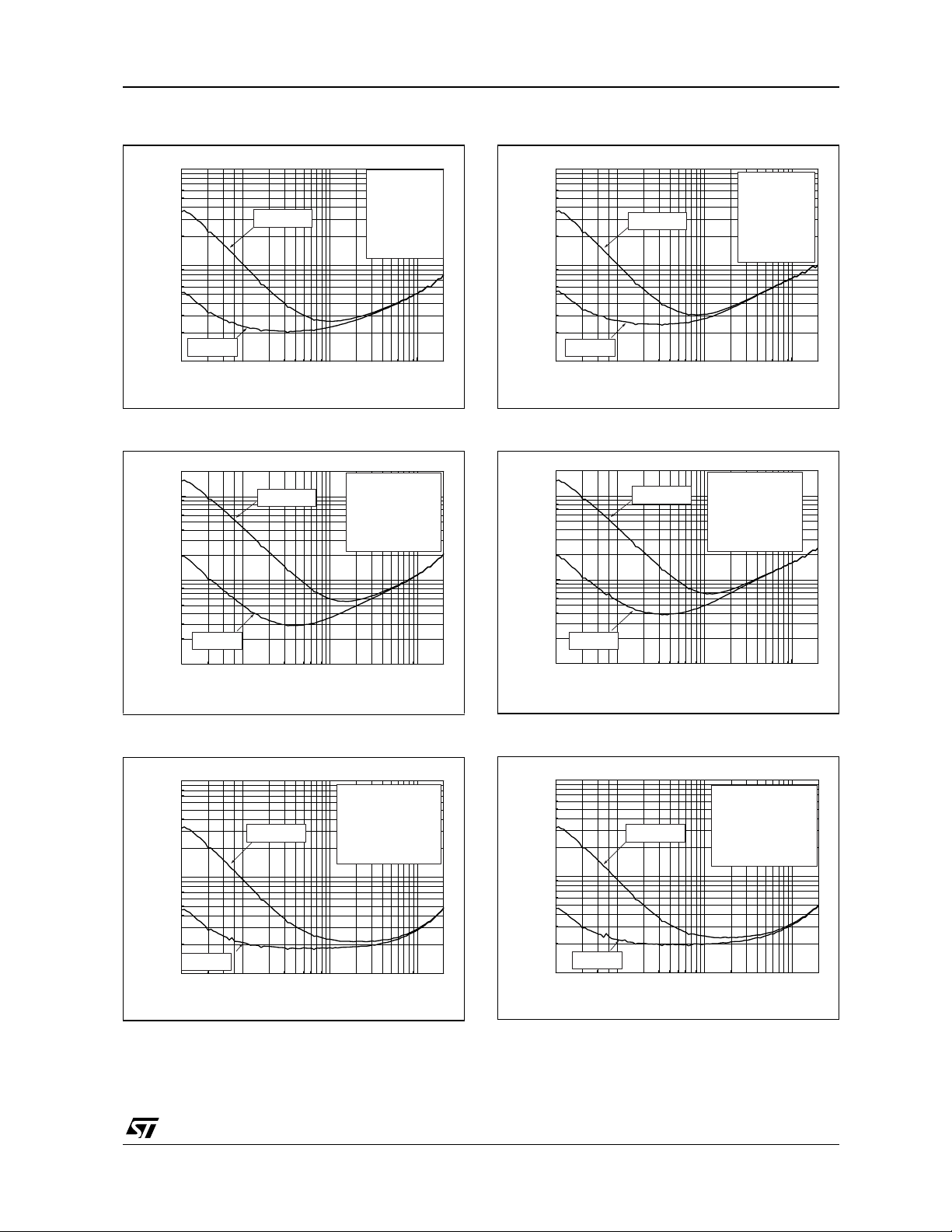
0.3 1 10 100 1000 10000
-40
-20
0
20
40
60
80
-240
-220
-200
-180
-160
-140
-120
-100
-80
-60
-40
-20
0
Gain (dB)
Frequency (kHz)
Vcc = 3.3V
ZL = 8Ω + 560pF
Tamb = 25°C
Gain
Phase
Phase (Deg)
0.3 1 10 100 1000 10000
-40
-20
0
20
40
60
80
-240
-220
-200
-180
-160
-140
-120
-100
-80
-60
-40
-20
0
Gain (dB)
Frequency (kHz)
Vcc = 2.6V
ZL = 8Ω + 560pF
Tamb = 25°C
Gain
Phase
Phase (Deg)
Fig. 1 : Open Loop Frequency Response
0
60
40
Phase
20
Gain (dB)
0
-20
-40
0.3 1 10 100 1000 10000
Gain
Frequency (kHz)
Vcc = 5V
RL = 8
Tamb = 25°C
Ω
-20
-40
-60
-80
-100
-120
-140
-160
-180
-200
-220
Fig. 3 : Open Loop Frequency Response
80
60
40
20
Gain (dB)
0
-20
-40
0.3 1 10 100 1000 10000
Gain
Phase
Frequency (kHz)
Vcc = 3.3V
RL = 8
Ω
Tamb = 25°C
0
-20
-40
-60
-80
-100
-120
-140
-160
-180
-200
-220
-240
Phase (Deg)
Phase (Deg)
Fig. 2 : Open Loop Frequency Response
0
60
40
Gain
Vcc = 5V
ZL = 8Ω + 560pF
Tamb = 25°C
Phase
20
-20
-40
-60
-80
-100
-120
Gain (dB)
0
-140
-160
-20
-180
-200
-40
0.3 1 10 100 1000 10000
Frequency (kHz)
-220
Fig. 4 : Open Loop Frequency Response
Phase (Deg)
Fig. 5 : Open Loop Frequency Response
80
60
40
Phase
20
Gain (dB)
0
-20
-40
0.3 1 10 100 1000 10000
6/29
Gain
Frequency (kHz)
Vcc = 2.6V
RL = 8
Tamb = 25°C
Fig. 6 : Open Loop Frequency Response
0
-20
-40
Ω
-60
-80
-100
-120
-140
-160
Phase (Deg)
-180
-200
-220
-240
TS4872
Fig. 7 : Open Loop Frequency Response
100
80
60
Gain
40
20
Gain (dB)
0
Vcc = 5V
CL = 560pF
-20
Tamb = 25°C
-40
0.3 1 10 100 1000 10000
Phase
Frequency (kHz)
-80
-100
-120
-140
-160
-180
-200
-220
Fig. 9 : Open Loop Frequency Response
100
80
60
Gain
40
20
Gain (dB)
0
Vcc = 2.6V
-20
CL = 560pF
Tamb = 25°C
-40
0.3 1 10 100 1000 10000
Phase
Frequency (kHz)
-80
-100
-120
-140
-160
-180
-200
-220
-240
Phase (Deg)
Phase (Deg)
Fig. 8 : Open Loop Frequency Response
100
80
60
Gain
40
20
Gain (dB)
0
Vcc = 3.3V
CL = 560pF
-20
Tamb = 25°C
-40
0.3 1 10 100 1000 10000
Phase
Frequency (kHz)
-80
-100
-120
-140
-160
-180
-200
-220
-240
Phase (Deg)
7/29
TS4872
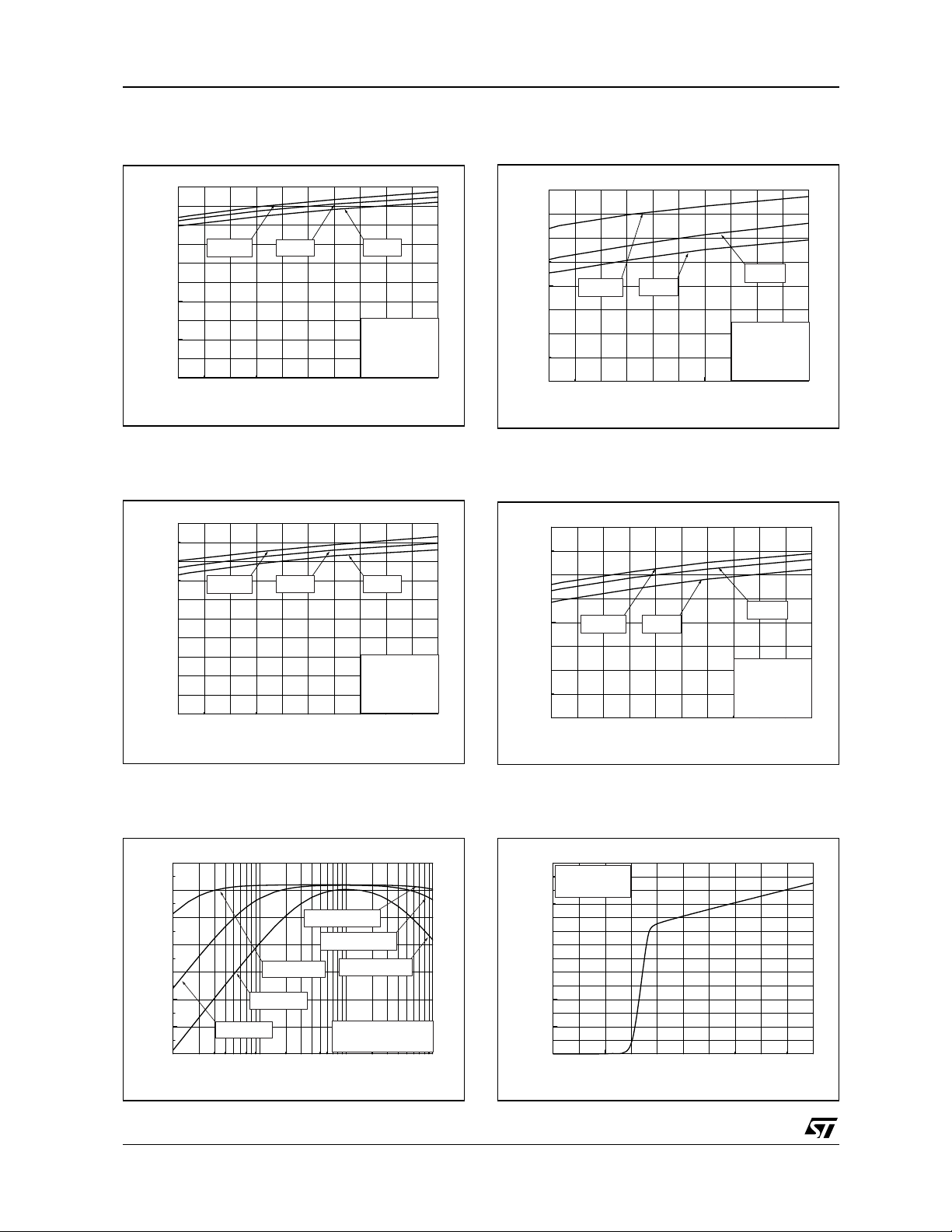
10 100 1000 10000 100000
-60
-50
-40
-30
-20
-10
Cin=22nF
Cin=100nF
Cin=220nF
Cin=330nF
Cin=1µF
Vcc = 5 & 2.6V
Rfeed = 22k, Rin = 22k
Cb = 1µF
Rg = 100Ω, RL = 8
Ω
Tamb = 25°C
PSRR (dB)
Frequency (Hz)
Fig. 10 : Power Supply Rejection Ratio (PSRR)
vs Power Supply
-30
Rfeed = 22k
Cb = 1µF & 0.1µF
-40
Input = floating
RL = 8
Tamb = 25°C
-50
PSRR (dB)
-60
Vcc=5V
Ripple=200mVrms
-70
-80
10 100 1000 10000 100000
Ω
Ω
Vcc=3.3V
Ripple=100mVrms
Vcc=2.6V
Ripple=200mVrms
Frequency (Hz)
Fig. 12 : Power Supply Rejection Ratio (PSRR)
vs Bypass Capacitor
-10
-20
-30
-40
-50
PSRR (dB)
-60
Cb=1µF
Cb=10µF
Vcc = 5 & 2.6V
Rfeed = 22k
Rin = 22k, Cin = 1µF
Rg = 100Ω, RL = 8
Tamb = 25°C
Cb=47µF
Ω
Fig. 11 : Power Supply Rejectio n Ratio (PSRR)
vs Feedback Capacitor
-10
Vcc = 5V
-20
Cb = 1µF & 0.1µF
Rfeed = 22k
-30
Rfeed = 22k
Vripple = 200mVms
Input = floating
-40
RL = 8
Tamb = 25°C
-50
PSRR (dB)
-60
-70
-80
10 100 1000 10000 100000
Ω
Ω
Ω
Frequency (Hz)
Cfeed=0
Cfeed=150pF
Cfeed=330pF
Cfeed=680pF
Fig. 13 : Power Supply Rejectio n Ratio (PSRR)
vs Input Capacitor
-70
Cb=100µF
-80
10 100 1000 10000 100000
Frequency (Hz)
Fig. 14 : Power Supply Rejection Ratio (PSRR)
vs Feedback Resistor
-10
Vcc = 5V
-20
Cb = 1µF & 0.1µF
Vripple = 200mVrms
-30
Input = floating
RL = 8
-40
-50
PSRR (dB)
8/29
-60
-70
-80
Ω
Tamb = 25°C
10 100 1000 10000 100000
Rfeed=22k
Frequency (Hz)
Rfeed=110k
Rfeed=47k
Ω
Ω
Ω
Rfeed=10k
Ω

TS4872
Fig. 15 : Pout @ THD + N = 1% vs Supply
Voltage vs RL
1.4
8
Gv = 2 & 10
1.2
Cb = 1µF
F = 1kHz
1.0
BW < 125kHz
Tamb = 25°C
0.8
0.6
0.4
0.2
Output power @ 1% THD + N (W)
0.0
2.5 3.0 3.5 4.0 4.5 5.0
4
Vcc (V)
Ω
Ω
6
Ω
16
Ω
32
Ω
Fig. 17 : Power Dissipation vs Pout
1.4
Vcc=5V
F=1kHz
1.2
THD+N<1%
1.0
0.8
0.6
Power Dissipation (W)
0.4
0.2
0.0
0.0 0.2 0.4 0.6 0.8 1.0 1.2 1.4
RL=16
Ω
Output Power (W)
RL=4
RL=8
Ω
Fig. 16 : Pout @ THD + N = 10% vs Supply
Voltage vs RL
2.0
Gv = 2 & 10
1.8
Cb = 1µF
F = 1kHz
1.6
BW < 125kHz
1.4
Tamb = 25°C
1.2
1.0
0.8
0.6
0.4
Output power @ 10% THD + N (W)
0.2
0.0
2.5 3.0 3.5 4.0 4.5 5.0
4Ω
Vcc (V)
8Ω
6Ω
16Ω
32Ω
Fig. 18 : Power Dissipation vs Pout
0.6
Vcc=3.3V
F=1kHz
0.5
Ω
THD+N<1%
0.4
0.3
0.2
Power Dissipation (W)
0.1
RL=16
0.0
0.0 0.2 0.4 0.6 0.8
Ω
Output Power (W)
RL=8
RL=4
Ω
Ω
Fig. 19 : Power Dissipation vs Pout
0.40
Vcc=2.6V
0.35
F=1kHz
THD+N<1%
0.30
0.25
0.20
0.15
Power Dissipation (W)
0.10
0.05
0.00
0.0 0.1 0.2 0.3 0.4
RL=16
RL=8
Ω
Output Power (W)
RL=4
Ω
Fig. 20 : Power Derating Curves
1.4
1.2
Ω
1.0
0.8
0.6
0.4
0.2
Flip-Chip Package Power Dissipation (W)
0.0
No Heat sink
0 25 50 75 100 125 150
Ambiant Temperature ( C)
Heat sink surface = 125mm
(See demoboard)
2
9/29

TS4872
1E-3 0.01 0.1 1
0.01
0.1
1
10
Rl = 4Ω, Vcc = 5V
Gv = 10
Cb = Cin = 1µF
BW < 125kHz, Tamb = 25°C
20kHz
20Hz
1kHz
THD + N (%)
Output Power (W)
1E-3 0.01 0.1
0.01
0.1
1
10
Rl = 4Ω, Vcc = 2.6V
Gv = 10
Cb = Cin = 1µF
BW < 125kHz
Tamb = 25°C
20kHz
20Hz
1kHz
THD + N (%)
Output Power (W)
Fig. 21 : THD + N vs Output Power
10
Rl = 4
Ω
Vcc = 5V
Gv = 2
Cb = Cin = 1µF
1
BW < 125kHz
Tamb = 25°C
THD + N (%)
0.1
0.01
1E-3 0.01 0.1 1
20kHz
20Hz
Output Power (W)
1kHz
Fig. 23 : THD + N vs Output Power
10
Rl = 4Ω, Vcc = 3.3V
Gv = 2
Cb = Cin = 1µF
BW < 125kHz
1
Tamb = 25°C
20kHz
THD + N (%)
0.1
Fig. 22 : THD + N vs Output Power
Fig. 24 : THD + N vs Output Power
10
Rl = 4Ω, Vcc = 3.3V
Gv = 10
Cb = Cin = 1µF
1
THD + N (%)
0.1
BW < 125kHz
Tamb = 25°C
20kHz
20Hz
Fig. 25 : THD + N vs Output Power
20Hz
0.01
1E-3 0.01 0.1 1
10
Rl = 4Ω, Vcc = 2.6V
Gv = 2
Cb = Cin = 1µF
BW < 125kHz
1
Tamb = 25°C
THD + N (%)
0.1
0.01
1E-3 0.01 0.1
Output Power (W)
20kHz
20Hz
1kHz
Output Power (W)
1kHz
1kHz
0.01
1E-3 0.01 0.1 1
Output Power (W)
Fig. 26 : THD + N vs Output Power
10/29
TS4872
1E-3 0.01 0.1 1
0.01
0.1
1
10
Rl = 8
Ω
Vcc = 5V
Gv = 10
Cb = Cin = 1µF
BW < 125kHz
Tamb = 25°C
20kHz
20Hz
1kHz
THD + N (%)
Output Power (W)
1E-3 0.01 0.1
0.01
0.1
1
10
Rl = 8Ω, Vcc = 2.6V
Gv = 10
Cb = Cin = 1µF
BW < 125kHz
Tamb = 25°C
20kHz
20Hz
1kHz
THD + N (%)
Output Power (W)
Fig. 27 : THD + N vs Output Power
10
Rl = 8
Ω
Vcc = 5V
Gv = 2
Cb = Cin = 1µF
1
BW < 125kHz
Tamb = 25°C
THD + N (%)
0.1
0.01
1E-3 0.01 0.1 1
20Hz
20kHz
1kHz
Output Power (W)
Fig. 29 : THD + N vs Output Power
10
Rl = 8Ω, Vcc = 3.3V
Gv = 2
Cb = Cin = 1µF
BW < 125kHz
1
Tamb = 25°C
THD + N (%)
0.1
20Hz
20kHz
Fig. 28 : THD + N vs Output Power
Fig. 30 : THD + N vs Output Power
10
Rl = 8Ω, Vcc = 3.3V
Gv = 10
Cb = Cin = 1µF
BW < 125kHz
1
Tamb = 25°C
20Hz
THD + N (%)
0.1
20kHz
0.01
1E-3 0.01 0.1 1
1kHz
Output Power (W)
Fig. 31 : THD + N vs Output Power
10
Rl = 8Ω, Vcc = 2.6V
Gv = 2
Cb = Cin = 1µF
BW < 125kHz
1
Tamb = 25°C
THD + N (%)
0.1
0.01
1E-3 0.01 0.1
1kHz
20Hz
Output Power (W)
20kHz
1kHz
0.01
1E-3 0.01 0.1 1
Output Power (W)
Fig. 32 : THD + N vs Output Power
11/29

TS4872
1E-3 0.01 0.1 1
0.01
0.1
1
10
Rl = 8Ω, Vcc = 5V, Gv = 10
Cb = 0.1µF, Cin = 1µF
BW < 125kHz, Tamb = 25°C
20kHz
20Hz
1kHz
THD + N (%)
Output Power (W)
1E-3 0.01 0.1
0.01
0.1
1
10
Rl = 8Ω, Vcc = 2.6V, Gv = 10
Cb = 0.1µF, Cin = 1µF
BW < 125kHz, Tamb = 25°C
20kHz
20Hz
1kHz
THD + N (%)
Output Power (W)
Fig. 33 : THD + N vs Output Power
10
Rl = 8
Ω
Vcc = 5V
Gv = 2
Cb = 0.1µF, Cin = 1µF
1
BW < 125kHz
Tamb = 25°C
THD + N (%)
0.1
0.01
1E-3 0.01 0.1 1
20kHz
Output Power (W)
20Hz
1kHz
Fig. 35 : THD + N vs Output Power
10
Rl = 8Ω, Vcc = 3.3V
Gv = 2
Cb = 0.1µF, Cin = 1µF
BW < 125kHz
1
Tamb = 25°C
THD + N (%)
0.1
20Hz
20kHz
Fig. 34 : THD + N vs Output Power
Fig. 36 : THD + N vs Output Power
10
Rl = 8Ω, Vcc = 3.3V, Gv = 10
Cb = 0.1µF, Cin = 1µF
BW < 125kHz, Tamb = 25°C
1
20Hz
20kHz
THD + N (%)
0.1
0.01
1E-3 0.01 0.1 1
1kHz
Output Power (W)
Fig. 37 : THD + N vs Output Power
10
Rl = 8Ω, Vcc = 2.6V
Gv = 2
Cb = 0.1µF, Cin = 1µF
BW < 125kHz
1
Tamb = 25°C
THD + N (%)
0.1
0.01
1E-3 0.01 0.1
1kHz
12/29
20Hz
Output Power (W)
20kHz
1kHz
0.01
1E-3 0.01 0.1 1
Output Power (W)
Fig. 38 : THD + N vs Output Power

TS4872
1E-3 0.01 0.1 1
0.01
0.1
1
10
Rl = 16Ω, Vcc = 5V
Gv = 10
Cb = Cin = 1µF
BW < 125kHz
Tamb = 25°C
20kHz
20Hz
1kHz
THD + N (%)
Output Power (W)
Fig. 39 : THD + N vs Output Power
10
Rl = 16Ω, Vcc = 5V
Gv = 2
Cb = Cin = 1µF
1
BW < 125kHz
Tamb = 25°C
0.1
THD + N (%)
0.01
1kHz
1E-3 0.01 0.1 1
20Hz
Output Power (W)
20kHz
Fig. 41 : THD + N vs Output Power
10
Rl = 16Ω, Vcc = 3.3V
Gv = 2
Cb = Cin = 1µF
1
BW < 125kHz
Tamb = 25°C
0.1
THD + N (%)
1kHz
0.01
1E-3 0.01 0.1
20Hz
20kHz
Output Power (W)
Fig. 40 : THD + N vs Output Power
Fig. 42 : THD + N vs Output Power
10
Rl = 16
Ω
Vcc = 3.3V
Gv = 10
Cb = Cin = 1µF
1
BW < 125kHz
Tamb = 25°C
20Hz
THD + N (%)
0.1
20kHz
1kHz
0.01
1E-3 0.01 0.1
Output Power (W)
Fig. 43 : THD + N vs Output Power
10
Rl = 16
Ω
Vcc = 2.6V
Gv = 2
Cb = Cin = 1µF
1
BW < 125kHz
Tamb = 25°C
0.1
THD + N (%)
0.01
1E-3 0.01 0.1
20Hz
1kHz
Output Power (W)
20kHz
Fig. 44 : THD + N vs Output Power
10
Rl = 16
Ω
Vcc = 2.6V
Gv = 10
Cb = Cin = 1µF
1
BW < 125kHz
Tamb = 25°C
THD + N (%)
0.1
20kHz
0.01
1E-3 0.01 0.1
1kHz
20Hz
Output Power (W)
13/29

TS4872
20 100 1000 10000
0.01
0.1
1
RL = 4Ω, Vcc = 5V
Gv = 10
Cb = 1µF
BW < 125kHz
Tamb = 25°C
Pout = 600mW
Pout = 1.2W
THD + N (%)
Frequency (Hz)
20 100 1000 10000
0.01
0.1
1
RL = 4Ω, Vcc = 3.3V
Gv = 10
Cb = 1µF
BW < 125kHz
Tamb = 25°C
Pout = 270mW
Pout = 540mW
THD + N (%)
Frequency (Hz)
20 100 1000 10000
0.01
0.1
1
RL = 4Ω, Vcc = 2.6V
Gv = 10
Cb = 1µF
BW < 125kHz
Tamb = 25°C
Pout = 240 & 120mW
THD + N (%)
Frequency (Hz)
Fig. 45 : THD + N vs Frequency
RL = 4Ω, Vcc = 5V
1
Gv = 2
Cb = 1µF
BW < 125kHz
Tamb = 25°C
0.1
THD + N (%)
0.01
20 100 1000 10000
Frequency (Hz)
Pout = 1.2W
Fig. 47 : THD + N vs Frequency
RL = 4Ω, Vcc = 3.3V
1
Gv = 2
Cb = 1µF
BW < 125kHz
Tamb = 25°C
0.1
THD + N (%)
Pout = 540mW
Fig. 46 : THD + N vs Frequency
Pout = 600mW
Fig. 48 : THD + N vs Frequency
0.01
20 100 1000 10000
Fig. 49 : THD + N vs Frequency
RL = 4Ω, Vcc = 2.6V
1
Gv = 2
Cb = 1µF
BW < 125kHz
Tamb = 25°C
Pout = 240 & 120mW
0.1
THD + N (%)
0.01
20 100 1000 10000
Pout = 270mW
Frequency (Hz)
Fig. 50 : THD + N vs Frequency
Frequency (Hz)
14/29
TS4872
20 100 1000 10000
0.01
0.1
1
Cb = 1µF
Cb = 0.1µF
RL = 8
Ω
Vcc = 5V
Gv = 2
Pout = 450mW
BW < 125kHz
Tamb = 25°C
THD + N (%)
Frequency (Hz)
20 100 1000 10000
0.01
0.1
1
Cb = 1µF
Cb = 0.1µF
RL = 8Ω, Vcc = 5V
Gv = 10
Pout = 450mW
BW < 125kHz
Tamb = 25°C
THD + N (%)
Frequency (Hz)
20 100 1000 10000
0.01
0.1
1
Cb = 1µF
Cb = 0.1µF
RL = 8Ω, Vcc = 3.3V
Gv = 2
Pout = 200mW
BW < 125kHz
Tamb = 25°C
THD + N (%)
Frequency (Hz)
Fig. 51 : THD + N vs Frequency
1
Cb = 0.1µF
0.1
THD + N (%)
Cb = 1µF
0.01
20 100 1000 10000
Frequency (Hz)
Fig. 53 : THD + N vs Frequency
1
Cb = 0.1µF
RL = 8Ω, Vcc = 5V
Gv = 10
Pout = 900mW
BW < 125kHz
Tamb = 25°C
RL = 8
Ω
Vcc = 5V
Gv = 2
Pout = 900mW
BW < 125kHz
Tamb = 25°C
Fig. 52 : THD + N vs Frequency
Fig. 54 : THD + N vs Frequency
0.1
THD + N (%)
Cb = 1µF
0.01
20 100 1000 10000
Fig. 55 : THD + N vs Frequency
1
0.1
THD + N (%)
Cb = 1µF
0.01
20 100 1000 10000
Frequency (Hz)
Cb = 0.1µF
Frequency (Hz)
Fig. 56 : THD + N vs Frequency
RL = 8Ω, Vcc = 3.3V
Gv = 2
Pout = 400mW
BW < 125kHz
Tamb = 25°C
15/29

TS4872
20 100 1000 10000
0.01
0.1
1
Cb = 1µF
Cb = 0.1µF
RL = 8Ω, Vcc = 3.3V
Gv = 10
Pout = 200mW
BW < 125kHz
Tamb = 25°C
THD + N (%)
Frequency (Hz)
20 100 1000 10000
0.01
0.1
1
Cb = 1µF
Cb = 0.1µF
RL = 8Ω, Vcc = 2.6V
Gv = 10
Pout = 110mW
BW < 125kHz
Tamb = 25°C
THD + N (%)
Frequency (Hz)
20 100 1000 10000
0.01
0.1
1
Cb = 0.1µF
Cb = 1µF
RL = 8Ω, Vcc = 2.6V
Gv = 10
Pout = 110mW
BW < 125kHz
Tamb = 25°C
THD + N (%)
Frequency (Hz)
Fig. 57 : THD + N vs Frequency
1
0.1
THD + N (%)
Cb = 1µF
0.01
20 100 1000 10000
Cb = 0.1µF
Frequency (Hz)
RL = 8Ω, Vcc = 3.3V
Gv = 10
Pout = 400mW
BW < 125kHz
Tamb = 25°C
Fig. 59 : THD + N vs Frequency
1
RL = 8Ω, Vcc = 2.6V
Gv = 2
Pout = 220mW
Cb = 0.1µF
0.1
THD + N (%)
BW < 125kHz
Tamb = 25°C
Fig. 58 : THD + N vs Frequency
Fig. 60 : THD + N vs Frequency
Cb = 1µF
0.01
20 100 1000 10000
Fig. 61 : THD + N vs Frequency
1
0.1
THD + N (%)
Cb = 1µF
0.01
20 100 1000 10000
16/29
Frequency (Hz)
Cb = 0.1µF
Frequency (Hz)
Fig. 62 : THD + N vs Frequency
RL = 8Ω, Vcc = 2.6V
Gv = 10
Pout = 220mW
BW < 125kHz
Tamb = 25°C

TS4872
20 100 1000 10000
0.01
0.1
RL = 16Ω, Vcc = 5V
Gv = 10, Cb = 1µF
BW < 125kHz
Tamb = 25°C
Pout = 310mW
Pout = 620mW
THD + N (%)
Frequency (Hz)
20 100 1000 10000
0.01
0.1
1
RL = 16Ω, Vcc = 3.3V
Gv = 10, Cb = 1µF
BW < 125kHz
Tamb = 25°C
Pout = 135mW
Pout = 270mW
THD + N (%)
Frequency (Hz)
20 100 1000 10000
0.01
0.1
1
RL = 16Ω, Vcc = 2.6V
Gv = 10, Cb = 1µF
BW < 125kHz
Tamb = 25°C
Pout = 80mW
Pout = 160mW
THD + N (%)
Frequency (Hz)
Fig. 63 : THD + N vs Frequency
0.1
Pout = 310mW
0.01
THD + N (%)
1E-3
Pout = 620mW
20 100 1000 10000
Frequency (Hz)
RL = 16Ω, Vcc = 5V
Gv = 2, Cb = 1µF
BW < 125kHz
Tamb = 25°C
Fig. 65 : THD + N vs Frequency
0.1
Pout = 135mW
0.01
THD + N (%)
Pout = 270mW
1E-3
20 100 1000 10000
Frequency (Hz)
RL = 16Ω, Vcc = 3.3V
Gv = 2, Cb = 1µF
BW < 125kHz
Tamb = 25°C
Fig. 64 : THD + N vs Frequency
Fig. 66 : THD + N vs Frequency
Fig. 67 : THD + N vs Frequency
0.1
0.01
THD + N (%)
1E-3
Pout = 160mW
20 100 1000 10000
Fig. 68 : THD + N vs Frequency
Pout = 80mW
RL = 16Ω, Vcc = 2.6V
Gv = 2, Cb = 1µF
BW < 125kHz
Tamb = 25°C
Frequency (Hz)
17/29
TS4872
2.5 3.0 3.5 4 .0 4.5 5.0
50
60
70
80
90
RL=16
Ω
RL=4
Ω
RL=8
Ω
Gv = 10
Cb = Cin = 1µF
THD+N < 0.7%
Tamb = 25°C
SNR (dB)
Vcc (V)
2.5 3.0 3.5 4 .0 4.5 5.0
60
70
80
90
100
RL=16Ω
RL=4Ω
RL=8Ω
Gv = 10
Cb = Cin = 1µF
THD+N < 0.7%
Tamb = 25°C
SNR (dB)
Vcc (V)
012345
0
1
2
3
4
5
6
7
Vstandby = 0V
Tamb = 25°C
Icc (mA)
Vcc (V)
Fig. 69 : Signal to Noise Ratio vs Power Supply
with Unweighted Filter (20Hz to 20kHz)
100
90
RL=4
RL=8
RL=16
80
70
SNR (dB)
60
50
2.5 3.0 3.5 4.0 4.5 5.0
Ω
Ω
Vcc (V)
Ω
Gv = 2
Cb = Cin = 1µF
THD+N < 0.4%
Tamb = 25°C
Fig. 71 : Signal to Noise Ratio vs Power Supply
with Weig h t e d Filt e r t y p e A
110
100
RL=4
RL=8
RL=16
90
Ω
Ω
Ω
Fig. 70 : Signa l to Nois e Ratio Vs Power Supply
with Unweighted Filter (20Hz to 20kHz)
Fig. 72 : Signal to Noise Ratio vs Power Supply
with Weighted Filter Type A
80
SNR (dB)
70
60
2.5 3.0 3.5 4.0 4.5 5.0
Vcc (V)
Fig. 73 : Frequency Response Gain vs Cin, &
Cfeed
10
5
0
-5
-10
Gain (dB)
-15
-20
-25
10 100 1000 10000
Cin = 82nF
18/29
Cin = 470nF
Cin = 22nF
Frequency (Hz)
Gv = 2
Cb = Cin = 1µF
THD+N < 0.4%
Tamb = 25°C
Fig. 74 : Current Consum ption vs Power
Supply Voltage
Cfeed = 330pF
Cfeed = 680pF
Cfeed = 2.2nF
Rin = Rfeed = 22kΩ
Tamb = 25°C

TS4872
2.5 3.0 3.5 4.0 4.5 5.0
0.0
0.1
0.2
0.3
0.4
0.5
0.6
0.7
0.8
0.9
1.0
Tamb = 25°C
RL = 16
Ω
RL = 8
Ω
RL = 4
Ω
Vout1 & Vout2
Clipping Voltage Low side (V)
Power supply Voltage (V)
Fig. 75 : C urrent Consumption v s St andby
Voltage @ Vcc = 5V
7
6
5
4
3
Icc (mA)
2
1
0
0.0 0.5 1.0 1.5 2.0 2.5 3.0 3.5 4.0 4.5 5.0
Vstandby (V)
Vcc = 5V
Tamb = 25°C
Fig. 77 : C urrent Consumption v s St andby
Voltage @ Vcc = 2.6V
6
5
Vcc = 2.6V
Tamb = 25°C
Fig. 76 : C urrent Consumption v s St andby
Voltage @ Vcc = 3.3V
6
5
4
3
Icc (mA)
2
1
0
0.0 0.5 1.0 1.5 2.0 2.5 3.0
Vstandby (V)
Vcc = 3.3V
Tamb = 25°C
Fig. 78 : Clipping Voltage vs Power Supply
Voltage and Load Resistor
4
3
Icc (mA)
2
1
0
0.0 0.5 1.0 1.5 2.0 2.5
Fig. 79 : Clipping Voltage vs Power Supply
Voltage and Load Resistor
1.0
0.9
Tamb = 25°C
0.8
0.7
0.6
0.5
0.4
Vout1 & Vout2
0.3
0.2
Clipping Voltage High side (V)
0.1
0.0
2.5 3.0 3.5 4.0 4.5 5.0
Vstandby (V)
Power supply Voltage (V)
RL = 8
RL = 4
Ω
RL = 16
Ω
Ω
19/29

TS4872
APPLICA TI ON INFORMATION
Fig. 80 : Demoboard Schematic
Vcc
S1
Vcc
S2
GND
C1
R2
C2
R1
Neg. input
J1
Neg. input
J2
Pos input
J3
Pos input
J4
Vcc
100k
R3
S5
PositiveInput mode
R7
C3
R4
C4 R5
S8
Standby
C5
+
C12
C11
1u
1u
+
Fig. 81 : Flip Chip Demoboard Components
Side
Vcc
C7
+
C6
100µ
6
1
Vin-
Vin+
7
R6
Bypass
3
Standby
5
C8
100n
Vcc
-
+
Bias
GND
2
Av=-1
+
100n
Vout1
Vout2
TS4872
U1
8
4
C9
+
470µ
C10
+
470µ
S6
OUT1
S3
GND
S4
GND
S7
Fig. 82 : Flip Chip Demoboard Top Layer
20/29

TS4872
)W(
R
)Vout2(
Pout
L
2
RMS
=
Fig. 83 : Flip C hip Demoboar d Bottom Layer
■BTL Configuration Principle
The TS4872 is a monolithic power amplifier with a
BTL output type. BTL (Bridge Tied Load) means
that each end of the load is connected to two
single ended output amplifiers. Thus, we have :
Single ended output 1 = Vout1 = Vout (V)
Single ended output 2 = Vout2 = -Vout (V)
And Vout1 - Vout2 = 2Vout (V)
The output power is :
The differential output voltage is
Vout2
V o ut 1 = 2Vin –
Rfeed
------------------- - (V)
Rin
The differential gain named gain (Gv) for more
convenient usage is :
Vout2 Vout1–
Gv =
--------------------------------------- = 2
Vin
Rfeed
------------------- Rin
Remark : Vout2 is in phase with Vin and Vout1 is
180 phased with Vin. It means that the positive
terminal of the l oudspeaker should be connected
to Vout2 and the negative to Vout1.
■Low and high frequency response
In low frequency region, the effect of Cin starts.
Cin with Rin forms a high pass filter with a -3dB cut
off frequency
FCL =
1
------------------------------- - Hz()
2π Rin Cin
In high frequency region, you can limit the
bandwidth by adding a capacitor (Cfeed) in parallel
on Rfeed. Its form a low pass filter with a -3dB cut
off frequency
CH =
F
---------------------------------------------- - Hz()
2π Rf eed Cfeed
1
■Power dissipation and efficiency
Hypothesis :
• Voltage and current in the load are sinusoidal
(Vout and Iout)
• Supply voltage is a pure DC source (Vcc)
For the same power supply voltage, the output
power in BTL configuration is four times higher
Regarding the load we have :
than the output power in single ended
configuration.
OUT = V
V
PEAK
sinωt (V)
■Gain In Typical Application Schematic (cf.
page 1)
In flat region (no effect of Cin), the output voltage
of the first stage is :
Vout1 = Vin –
Rfeed
------------------- - (V)
Rin
For the second stage : Vout2 = -Vout1 (V)
and
and
OUT =
I
P
OUT =
OUT
V
---------------- - (A)
L
R
PEAK
2R
2
L
V
---------------------- (W )
21/29

TS4872
)W(
R
Vcc2
maxPdiss
L
2
2
π
=
Then, the average current delivered by the supply
voltage is:
V
I
CC
AVG
= 2
PEAK
-------------------- (A)
πR
L
Then, the po wer dissip ated by the amplifier is
Pdiss = Psupply - Pout (W)
22Vcc
diss =
P
---------------------- P OUT POUT (W)–
L
πR
and the maximum value is obtained when:
∂Pdiss
--------------------- - = 0
∂P
OUT
and its value is:
Remark : This maximum valu e is only depending
on power supply voltage and load values.
The efficiency is the ratio between the output
power and the power supply
η =
OUT
P
----------------------- - =
Psupply
πV
PEAK
----------------------4VCC
The maximum theoret ical value is reached when
Vpeak = V c c, so
π
----- = 78. 5%
4
■Decoupl i ng of the ci rc u it
Two capacitors are needed to bypass properly the
TS4872. A power supply bypass capacitor Cs and
a bias voltage bypass capacitor Cb.
Cs has especially an influence on the THD+N in
high frequency (above 7kHz) and indirectly on the
power supply disturbances.
With 100µF, you can expect similar THD+N
performances like shown in the datasheet.
If Cs is lower than 100µF, in high frequency
increases, THD+N and disturbances on the power
supply rail are less filtered.
To the contrary, if Cs is higher than 100µF, those
disturbances on the power supply rail are more
filtered.
Cb has an influence on THD+N in lower frequency,
but its function is critical on the final result of PSRR
with input grounded in lower frequency.
If Cb is lower than 1µF, T HD+N increase in lower
frequency (see THD+N vs frequency curves) and
the PSRR worsens up
If Cb is higher than 1µF, the benefit on THD+N in
lower frequency is small but the ben efit on PSRR
is substantial (see PSRR vs. Cb curve : fig.12)
Note that Cin has a non-negligible effect on PSRR
in lower frequency. Lower is its value, higher is the
PSRR (see fig. 13).
■Pop a n d C lic k pe rformance
Pop and Click performance is intimately linked with
the size of the input capacitor Cin and the bias
voltage bypass capacitor Cb.
Size of Cin is due to th e lower cut off frequency
and PSRR value request and size of Cb is due to
THD+N and PSRR request always in lower
frequency.
Moreover, Cb determines the speed at which the
amplifier turns ON. The slow er the speed is , the
softer turns ON noise.
The charge time of Cb is directly proportional to
the internal generator resistance 50kΩ.
Then, the charging time constant for Cb is
τb = 50kΩxCb (s)
As Cb is directly connected to the non-inverting
input (pin 3 & 7) and if we want to minimize, in
amplitude and duration, the output spike on Vout1
(pin 8), Cin must be charged faster than Cb. T he
charge time constant of Cin is
τin = (Rin+Rfeed)xCin (s)
Thus we have the relation
τin << τb (s)
The respect of this relation permits to minimize the
pop and click noise.
Remark : Minimize Cin and Cb has a benefit on
pop and click phenomena but also on cost and
size of the application.
22/29

TS4872
Example
: your target for the -3dB cut off
frequency is 100 Hz. With Rin=Rfeed=22 kΩ,
Cin=72nF (in fact 82nF or 100nF).
With Cb=1µF, if you choose the one of the latest
two values of Cin, the pop and click phenomena at
power supply ON or standby function ON/OFF will
be very sma ll
50 kΩx1µF >> 44kΩx100nF (50ms >> 4.4ms).
Increase Cin value increases the pop and click
phenomena to an unpleasant sound at power
supply ON and standby function ON/OFF .
Why Cs is not important in pop and click
consideration ?
Hypothesis :
• Cs = 100µF
• Supply voltage = 5V
• Supply voltage internal resistor = 0.1Ω
• Supply current of the amplifier Icc = 6mA
At power ON of the supply, the supply capacitor is
charged through the internal power supply
resistor. So, to reach 5V you need about five to ten
times the charging time constant of Cs (τs =
0.1xCs (s)).
Then, this time equal 50µs to 100µs << τb in the
majority of application.
First of all, we must cal culate t he m inimum p ower
supply voltage to obtain 0.5W into 8Ω. With curves
in fig. 15, we can read 3.5V.
Thus, the power supply voltage value min. will be
3.5V.
Following the maximum power dissipation
equation
2
Vcc2
=
maxPdiss
2
π
R
)W(
L
with 3.5V we have Pdissmax=0.31W.
Referring to power derating curves (fig. 20), with
0.31W the maxim um ambien t temperature will be
100°C. This last value could be higher if you follow
the example layout shown on the demoboard
(better dissipation).
The gain of the amplifier in flat region will be
GV =
OUTPP
V
--------------------- =
VINPP
L POUT
22R
----------------------------------- - = 5.65
VINPP
We have Rin > 10kΩ. Let's take Rin = 10kΩ, then
Rfeed = 28.25kΩ. We could use for Rfeed = 30kΩ
in normalized value and th e gain will be Gv = 6.
At power OFF of the supply, Cs is discharged by a
constant current Icc. The di scharge time from 5V
to 0V of Cs is
t
DischCs =
5Cs
------------- - = 83 ms
Icc
Now, we must consider the discharge time of Cb.
At power OFF or standby ON, Cb is discharged by
a 100kΩ resistor. So the discharge time i s about
τb
≈ 3xCbx100kΩ (s).
Disch
In the majority of application, Cb=1µF, then
τb
≈300ms >> t
Disch
dischCs
.
■Power amplifier design examples
Given :
• Load impedance : 8Ω
• Output power @ 1% THD+N : 0.5W
• Input impedance : 10kΩ min.
• Input voltage peak to peak : 1Vpp
• Bandwidth frequency : 20Hz to 20kHz (0, -3dB)
• Ambient temperature max = 50°C
In lower frequency we want 20 Hz (-3dB cut off
frequency). Then
C IN =
1
------------------------------ = 795nF
2π
RinFCL
So, we could use for Cin a 1µF capacitor value that
gives 16Hz.
In Higher frequency we want 20k Hz (-3dB cut off
frequency). The Gain Bandwidth Product of the
TS4872 is 2MHz typical and doesn't change when
the amplifier delivers power into the load.
The first amplifier has a gain of
Rfeed
----------------- = 3
Rin
and the theoretical value of the -3dB cut-off higher
frequency is 2MHz/3 = 660kHz.
We can keep this value or limit the bandwidth by
adding a capacitor Cfeed, in parallel on Rfeed.
23/29

TS4872
Then
CFEED =
1
-------------------------------------- - = 265pF
2π R
FEEDFCH
So, we could use for Cfeed a 220pF capacitor
value that gives 24kHz.
Now, we can calculate the value of Cb with the
formula τb = 50kΩxCb >> τin = (Rin+Rfee d)xCin
which permits to redu ce t he po p and click effects.
Then Cb >> 0.8µF.
We can choose for Cb a normalized value of 2.2µF
that gives good results in THD+N and PSRR.
In the following tables, you could find three another
examples with values required for the demoboard.
Remark : components with (*) marking are
optional.
Application n°1 : 20Hz to 20kHz bandwidth and
6dB gain BTL power amplifier.
Components :
Designator Part Type
R1 22k / 0.125W
Application n°2 : 20Hz to 20kHz bandwidth and
20dB gai n BTL power am pl i fie r.
Components :
Designator Part Type
R1 110k / 0.125W
R4 22k / 0.125W
R6 Short Cicuit
R7 330k / 0.125W
C5 470nF
C6
C7 100nF
C9 Short Circuit
C10 Short Circuit
C12
S1, S2, S6, S7
S8
J1 SMB Plug
U1 TS4872IJ
100
µF
1
µF
2mm insulated Plug
10.16mm pitch
2 pts connector 2.54mm
pitch
R4 22k / 0.125W
R6 Short Cicuit
R7 330k / 0.125W
C5 470nF
C6
C7 100nF
C9 Short Circuit
C10 Short Circuit
C12
S1, S2, S6, S7
S8
J1 SMB plug
U1 TS4872IJ
24/29
100
µF
1
µF
2mm insulated Plug
10.16mm pitch
2 pts connector 2.54mm
pitch
Application n°3 : 50Hz to 10kHz bandwidth and
10dB gai n BTL power am pl i fie r.
Components :
Designator Part Type
R1 33k / 0.125W
R2 Short Circuit
R4 22k / 0.125W
R6 Short Cicuit
R7 330k / 0.125W
C2 470pF
C5 150nF
C6 100µF
C7 100nF
C9 Short Circuit

TS4872
Designator Part Type
C10 Short Circuit
C12 1µF
S1, S2, S6, S7
S8
J1 SMB Plug
U1 TS4872IJ
2mm insulated Plug
10.16mm pitch
2 pts connector 2.54mm
pitch
Application n°4 : Differential inputs BTL power
amplifier.
In this configuration, we need to place these
components : R1, R4, R5, R6, R7, C4, C5, C12.
We have also : R4 = R5, R1 = R6, C4 = C5.
The gain of the amplifier is :
G VDIFF = 2
R1
------- - (Pos. Input - Neg.Input)
R4
For a 20Hz to 20kHz bandwidth and 6dB gain BTL
power amplifier you could follow the bill of material
below .
Designator Part Type
C6 100µF
C7 100nF
C9 Short Circuit
C10 Short Circuit
C12 1µF
S1, S2, S6, S7
S8
J1, J3 SMB Plug
U1 TS4872IJ
2mm insulated Plug
10.16mm pitch
2 pts connector 2.54mm
pitch
■Note on how to use the PSRR curves
(page 8)
We have finished a design and we have ch osen
the components :
■ Rin=Rfeed=22kΩ
■ Cin=100nF
■ Cb=1µF
Components :
Designator Part Type
R1 22k / 0.125W
R4 22k / 0.125W
R5 22k / 0.125W
R6 22k / 0.125W
R7 330k / 0.125W
C4 470nF
C5 470nF
Now, on fig. 13, we can see the PSRR (input
grounded) vs frequency curves. At 217Hz we have
a PSRR value of -36dB.
In reality we want a value about -70dB. So, we
need a gain of 34dB !
Now, on fig. 12 we can see the effect of Cb on the
PSRR (input grounded) vs. frequency. With
Cb=100µF, we can reach the -70dB value.
The process to obtain the final curve (Cb=100µF,
Cin=100nF, Rin=Rfeed=22kΩ) is a simple transfer
point by point on each frequency of the curve on
fig. 13 to the curve on fig. 12.
The measurement results is shown on figu re 84.
25/29
TS4872
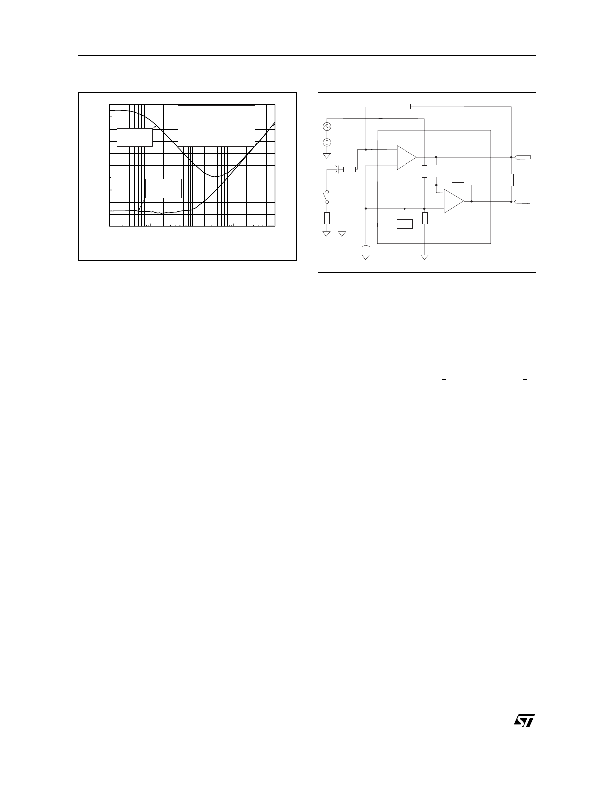
Fig. 84 : PSRR changes with Cb
-30
Cin=100nF
-40
Cb=1µF
-50
PSRR (dB)
-60
-70
10 100 1000 10000 100000
Cin=100nF
Cb=100µF
Vcc = 5 & 2.6V
Rfeed = 22k, Rin = 22k
Rg = 100Ω, RL = 8Ω
Tamb = 25°C
Frequency (Hz)
■Note on PSRR measurement
What is the PSRR ?
The PSRR is the Power Suppl y Rejection Ratio.
It’s a kind of SVR in a determined frequency
range. The PSRR of a device, is the ratio between
a power supply disturbance and the result on the
output.
Fig. 85 : PSRR measurement schematic
Rfeed
Vripple
Vcc
Rin
Cin
Rg
100 Ohms
1
Vin-
Vin+
7
Bypass
3
Standby
5
Cb
6
Vcc
-
+
Av=-1
+
Bias
GND
2
Vout1
Vout2
TS4872
8
4
■Principle of oper ation
• We fixed the DC voltage supply (Vcc)
• We fixed the AC sinusoidal ripple voltage
(Vripple)
• No bypass capacitor Cs is used
The PSRR value for each frequency is :
Vs-
RL
Vs+
We can say that the PSRR is the ability of a device
to minimize the impact of power supply
disturbances to the output.
How we measure the PSRR ?
For PSRR measurement schematic see figure 85
PSRR dB() = 20 x Log10
Rms V
---------------------------------------- ----Rms Vs
ripple()
- Vs
()
+
-
Remark : The measure of the Rms voltage is not a
Rms selective measure but a full range (2 Hz to
125 kHz) Rms measure. It means that we
measure the effective Rms signal + the noise.
26/29
TS4872
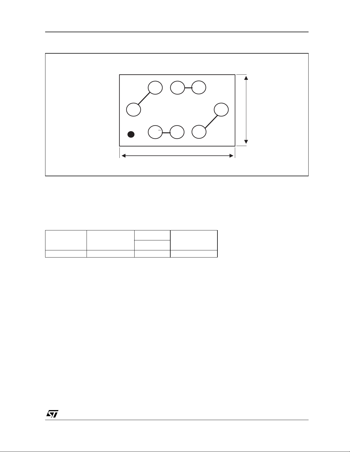
TOP VIEW OF THE DAISY CHAIN MECHANICAL DATA ( all drawings dimensions are in millimeters )
Vout1
8
76
+
Vin
Vin
Vcc
GND
12
3.02
5
STDBY
BYPASS
3
Vout2
1.52
4
REMARKS
Daisy chain sample is featuring pins connection two by two. The schematic above is illustrating the way
connecting pins each other. This sample is used for testing continuity on board. PCB needs to be designed
on the opposite way, where pin connections are not done on daisy chain samples. By that way, just
connecting an Ohmeter between pin 8 and pin 1, the soldering process continuity can be tested.
ORDER CODE
Part Number
TSDC4872IJT -40, +85°C
Temperature
Range
Package
J
•
Marking
DC01
27/29

TS4872
TAPE & REEL SPECIFICATION ( top view )
User direction of feed
76
8
12
76
8
12
5
XXX4872
4
3
5
XXX4872
4
3
28/29
PIN OUT (top view) MARKING (top view)
TS4872
8
Vout1
76
+
Vin
Vin
12
Vcc
GND
5
STDBY
BYPASS
3
■ Balls are underneath
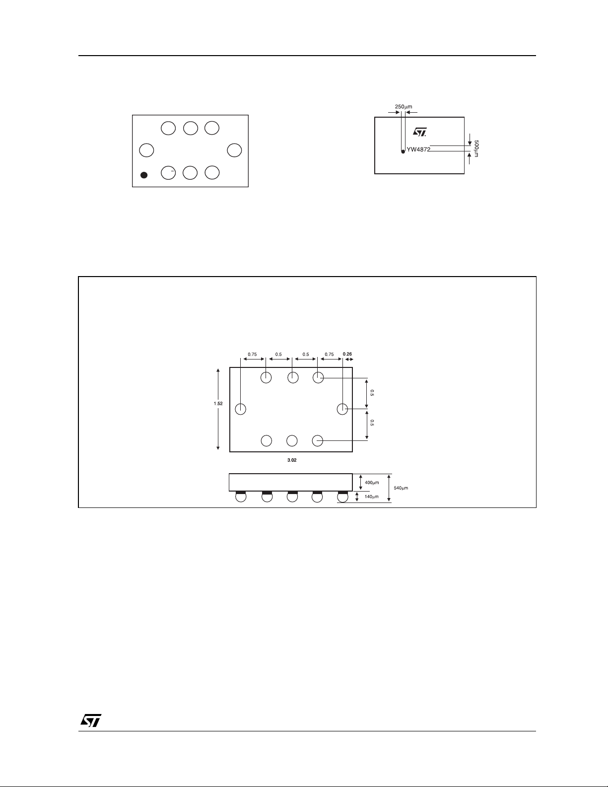
PACKAGE MECHANICAL DATA
FLIP CHIP - 8 BUMPS
■ Die size : (3.02mm±10%) x (1.52mm ±10%)
■ Die height (including bumps) : 540µm ±50µm
■ Bump height : 140µm ±15µm (i.e. bump diameter of 185µm ±15µm)
■ Silicon thickness : 400µm±25µm
■ Pitch: 500µm ±10µm and 750µm±1 0µm
Vout2
4
■ Y : Year
■ W : We ek wit h tw o d i gits
■ Example : 1254872
Information furnished is bel ieved to be accurate and reliable. However, STMicroe lectronics assumes no responsibility for the
consequences of use of such information nor for any infringement of patents or other rights of third parties which may result from
its use. No li cense is granted by i mp lication or otherwise under any patent or patent rights of STMicroelec tron ic s. S pec ificat ions
mentioned in this publication ar e subject to change without notice. This publication supersedes and replaces all information
previously supplied. S TMicroelectronics products are not authorized for use as critica l components in life suppo rt devices or
systems without express written approval of STMicroelectronics.
Australi a - Brazil - Canada - Chin a - F i nl and - France - Germany - Hong Kong - India - Israel - Italy - Japa n - Malaysia
Malta - Mor occo - Singapore - Spain - Sweden - S wi t zerland - U ni ted Kingdom - United Sta tes
© The ST logo is a registered trademark of STMicroelectronics
© 2001 STM icroelectronics - P r i n ted in Italy - All Rights Reserved
STMicr o el ectronics GROUP OF COMPA NI ES
© http://www.st.com
29/29
 Loading...