

TS4855
LOUDSPEAKER & HEADSET DRIVER
WITH VOLUME CONTROL
■ OPERA T ING FROM V
= 3.0 V to 5.0 V
CC
■ SPEAKER: Mono, THD+N @ 1 kHz is 1%
Max @ 1 W into 8
Ω BTL
■ HEADSET: Stereo, THD+N @ 1 kHz is 0.5%
Max. @ 85 mW into 32
Ω BTL
■ VOLUME CONTROL: 32-step digital
volume control
■ OUTPUT MODE: Eight different selections
■ Ultra low pop-and-click
■ Low Shutdown Current (0.1µA, typ.)
■ Thermal Shutdown Prot ec ti on
■ FLIP-CHIP Package 18 X 300 µm Bumps
DESCRIPTION
The TS4855 is a complete low power audio
amplifier solution targeted at mobile phones. It
integrates, into an extremely compact flip-chip
package, an audio amplifier, a speaker driver, and
a headset driver.
The Audio Power Amplifier can deliver 1.1 W
(typ.) of continuous RMS output power into an 8
speaker with a 1% THD+N value . To the headset
driver, the amplifier can deliver 85 mW (typ.) per
channel of continuous average power into stereo
32
Ω bridged-tied load with 0.5% THD+N @ 5 V.
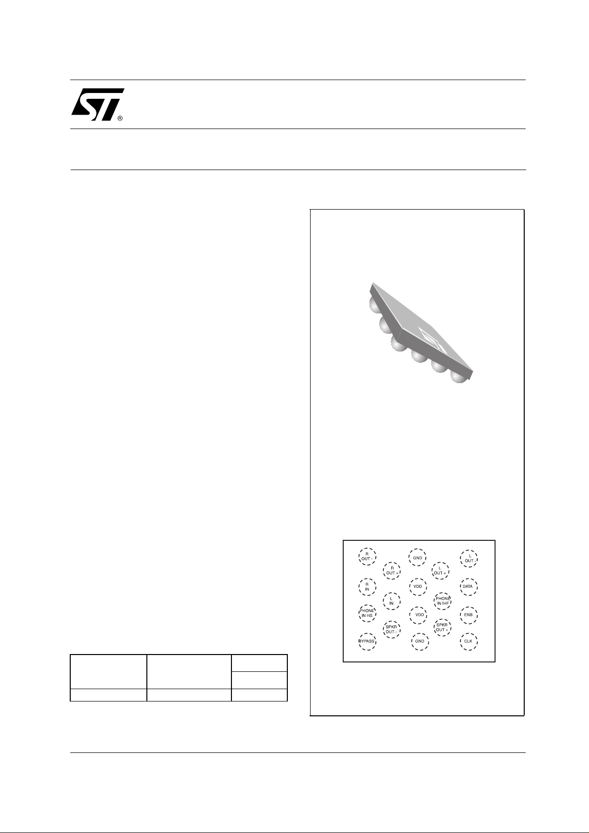
PIN CONNECTIONS (top view)
TS4855IJT - Flip Chip
Ω
Pin Out (top view)
This device features a 32-step digital volume
control and 8 different output selections. The
digital volume and output modes are controlled
through a three-digit SPI interface bus.
APPLICATIONS
• Mobile Phones
ORDER CODE
Part Number
TS4855IJT -40, +85°C
J = Flip Chip Package - only available in Tape & Reel (JT))
April 2003
Temperature
Range
Package
J
•
1/27
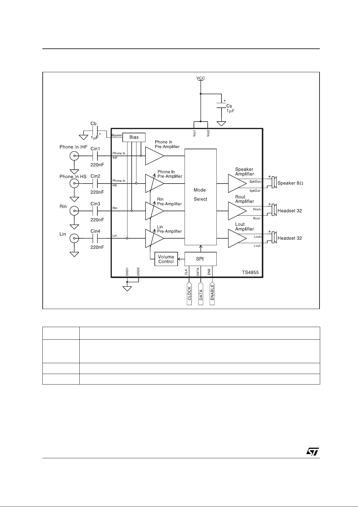
TS4855 Application Information for a Typical A pp lication
1 APPLICATION INFORMATION FOR A TYPICAL APPLICATION
External component descriptions
Component Functional Description
This is the input coupling capacitor. It blocks the DC voltage at, and couples the input signal to the
amplifier’s input terminals. Cin also creates a highpass filter with the internal input impedance Zin at
Fc = 1 / (2
This is the Supply Bypass capacitor. It provides power supply filtering.
This is the Bypass pin capacitor. It provides half-supply filtering.
π x Zin x Cin).
2/27
C
in
C
s
C
B
SPI Bus Interface TS4855
2 SPI BUS INTER FACE
2.1 Pin Descriptions
Pin Functional Description
DATA This is the serial data input pin
CLK This is the clock input pin
ENB This is the SPI enable pin active at high level
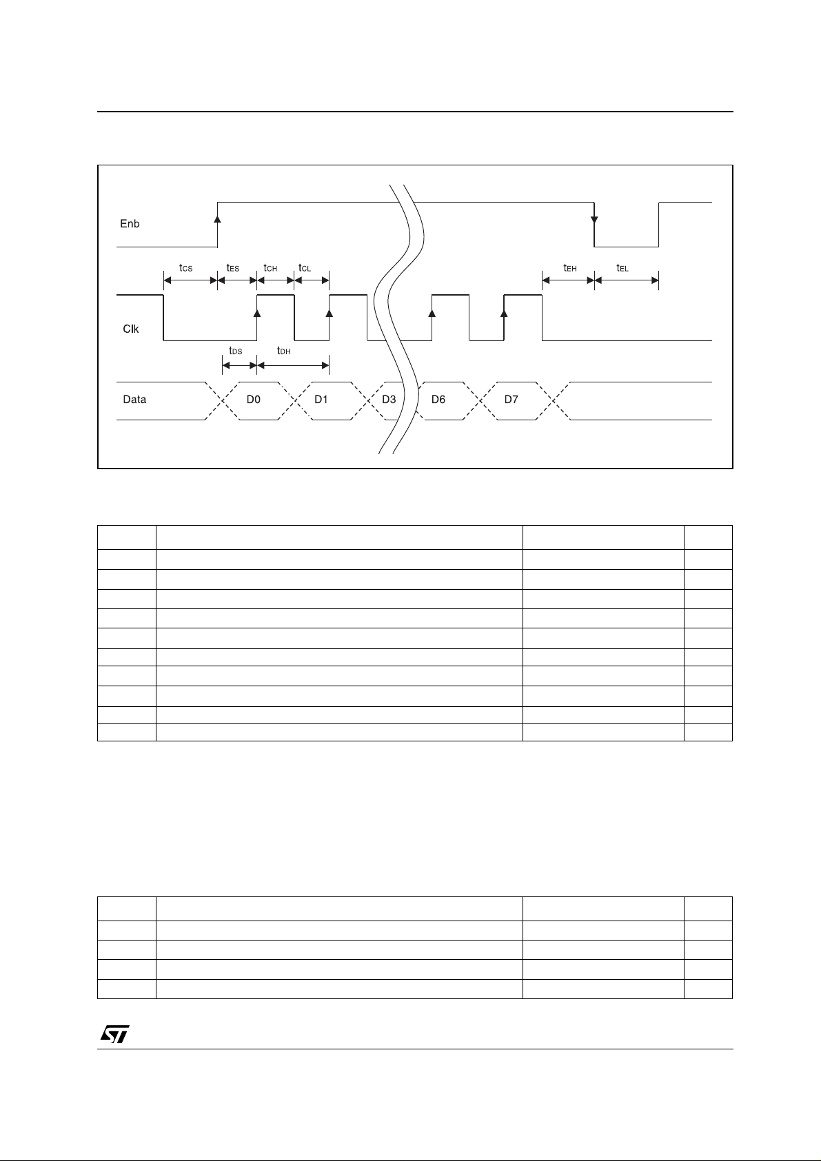
2.2 SPI Operation Description
The serial data bits are organized into a field
containing 8 bits of data as shown in
DATA 0 to DATA 2 bits determine the output
mode of the TS4855 as shown in
DATA 3 to DATA 7 bits determine the gain level
setting as illustrated by
Table 3
transfer, the data bits are written to the DATA pin
with the least significant bit (LSB) first. All serial
data are sampled at the rising edge of the CLK
signal. Once all the dat a bi ts h ave been sampled,
ENB transitions from logic-high to logic low to
complete the SPI sequence. All 8 bits must be
received before any data latch can occur. Any
excess CLK and DATA tran sitio ns w ill b e igno red
after the height rising clock edge has occurred.
For any data sequence longer than 8 bits, only the
Table 1
Table 2
. The
. The
. For each SPI
first 8 bits will get loaded into the shift register and
the rest of the bits will be disregarded.
Table 1 : Bit Allocation
DATA MODE S
LSB DATA 0 Mode 1
DATA 1 Mode 2
DATA 2 Mode 3
DATA 3 gain 1
DATA 4 gain 2
DATA 5 gain 3
DATA 6 gain 4
MSB DATA 7 gain 5
Table 2: Output Mode Selection
Output
Mode #
0 0 0 0 SD SD SD
10 0 1
2 0 1 0 MUTE
30 1 1
4 1 0 0 MUTE
51 0 1
6 1 1 0 MUTE
71 1 1
DATA 2 DATA 1 DATA 0
SPKR
+12dBxP
+12dBxP
+12dBxP
+12dBxP
out
IHF
IHF
IHF
IHF
R
out
SD SD
G1xP
HS
G1xP
HS
G2xR
in
G2xR
in
G2xR
G2xR
HS
+
in
in
G1xP
G1xPHS+
L
out
G1xP
HS
G1xP
HS
G2xL
in
G2xL
in
G1xPHS+
G2xL
in
G1xPHS+
G2xL
in
(SD = Shut Down Mode,
PHS = Non Filtered Phone In HS, P
= External High Pass Filtered Phone In IHF)
IHF
3/27

TS4855 SPI Bus Interface
Table 3: Gain Control Settings
G2: Gain (dB) G1: Gain (dB) DATA 7 DATA 6 DATA 5 DATA 4 DATA 3
-34.5 -40.5 0 0 0 0 0
-33.0 -39.0 0 0 0 0 1
-31.5 -37.5 0 0 0 1 0
-30.0 -36.0 0 0 0 1 1
-28.5 -34.5 0 0 1 0 0
-27.0 -33.0 0 0 1 0 1
-25.5 -31.5 0 0 1 1 0
-24.0 -30.0 0 0 1 1 1
-22.5 -28.5 0 1 0 0 0
-21.0 -27.0 0 1 0 0 1
-19.5 -25.5 0 1 0 1 0
-18.0 -24.0 0 1 0 1 1
-16.5 -22.5 0 1 1 0 0
-15.0 -21.0 0 1 1 0 1
-13.5 -19.5 0 1 1 1 0
-12.0 -18.0 0 1 1 1 1
-10.5 -16.5 1 0 0 0 0
-9.0 -15.0 1 0 0 0 1
-7.5 -13.5 1 0 0 1 0
-6.0 -12.0 1 0 0 1 1
-4.5 -10.5 1 0 1 0 0
-3.0 -9.0 1 0 1 0 1
-1.5 -7.5 1 0 1 1 0
0.0 -6.0 1 0 1 1 1
1.5 -4.5 1 1 0 0 0
3.0 -3.0 1 1 0 0 1
4.5 -1.5 1 1 0 1 0
6.0 0.0 1 1 0 1 1
7.5 1.5 1 1 1 0 0
9.0 3.0 1 1 1 0 1
10.5 4.5 1 1 1 1 0
12.0 6.0 1 1 1 1 1
4/27
Absolute Maximum Ratings TS4855
2.3 SPI Timing Diagram
3 ABSOLUTE MAXIMUM RATINGS
Symbol Parameter Value Unit
V
CC Supply voltage
T
T
R
Operating Free Air Temperature Range -40 to + 85 °C
oper
Storage Temperature -65 to +150 °C
stg
T
Maximum Junction Temperature 150 °C
j
Flip Chip Thermal Resistance Junction to Ambient
thja
1
2
6V
166 °C/W
Pd Power Dissipation Internally Limited
ESD
ESD
Human Body Model
Machine Model
4
3
2kV
100 V
Latch-up Immunity 200 mA
Lead Temperature (solde ring, 10sec ) 250 °C
1) All voltage values are measured with respect to the ground pin.
2) Device is protected in case of over temperature by a thermal shutdown active @ 150°C typ.
3) Human body model, 100pF discharged through a 1.5kΩ resistor into pin of device.
4) This is a minimum Value. Machine model ESD, a 200pF cap is charged to the specified voltage, then discharged directly into the IC with no external
series resistor (internal resistor < 5Ω), into pin to pin of device.
5.) All PSRR data limits are guaranteed by evaluation tests.
4 OPERATING CONDITIONS
Symbol Parameter Value Unit
V
V
V
Rin/VLin
T
Supply Voltage 3 to 5 V
CC
to VCC
Maximum Phone In Input Voltage
phin
Maximum Rin & Lin Input Voltage
Thermal Shutdown Temperature 150 °C
SD
G
ND
to V
G
ND
CC
V
V
5/27
TS4855 Electrical Characteristics
5 ELECTRICAL CHARACTERISTICS
Table 4: Electrical characteristics at VCC = +5 .0 V, GND = 0 V, Tamb = 25°C
(unless otherwise specified)
Symbol Parameter Min. Typ. Max. Unit
I
CC
I
STANDBY
Supply Current, all gain @ max settings
Output Mode 1, Vin = 0 V, no load
Output Mode 1, Vin = 0 V, loaded (8Ω)
Output Mode 2,3,4,5,6,7 Vin = 0 V, no loads
Output mode 2,3,4,5,6,7 Vin = 0 V, loaded (8Ω, 32Ω)
Standby Current
4.0
5.5
8.0
10
11
12
mA
8
9
µA
Output Mode 0 0.1 2
Voo Output Offset Voltage (differential)
Output Mode 1 to 7, Vin = 0 V, no load, Speaker Out
Output Mode 2 to 7 Vin = 0 V, no loads, Headset Out
5
5
20
40
mV
Vil “Logic low” input Voltage 0 0.4 V
Vih “Logic high” input Voltage 1.4 5 V
Po Output Pow e r
SPKR
R
out
, RL = 8Ω, THD+N = 1%, f = 1 kHz
out
& L
, RL = 32Ω, THD+N = 0.5%, f = 1 kHz
out
800701100
100
mW
THD + N Total Harmonic Distortion + Noise
R
& L
out
SPKR
R
out
SPKR
, Po = 70 mW, f = 1 kHz, RL = 32Ω
out
, Po = 800 mW, f = 1 kHz, RL = 8Ω
out
& L
, Po=50mW, 20Hz<f< 20kHz, RL=32Ω
out
, Po=400mW, 20Hz<f<20kHz, RL=8Ω
out
SNR S ignal To Noise Ratio
0.5
1
0.5
0.5
80 dB
A-Weighted, f = 1 k Hz
5)
PSRR
Power Supply Rejection Ratio
SPKR
;V ri ppl e= 200 mV Vpp, F= 217 Hz, In pu t Terminated 50Ω
out
Gain (BTL) = 12 dB, Output mode 1,3,5,7
R
& L
out
;Vripple = 200 mV Vpp, F = 217 Hz, Input T erminated 50Ω
out
Maximum gain setting, Output mode 2,3
& L
R
out
;Vripple = 200 mV Vpp, F = 217 Hz, Input T erminated 50Ω
out
Maximum gain setting, Output mode 4,5
R
& L
out
;Vripple = 200 mV Vpp, F = 217 Hz, Input T erminated 50Ω
out
Maximum gain setting, Output mode 6,7
58
52
50
46
61
55
53
49
dB
%
G2 Digital Gain Range (Rin & Lin) to R
out
G1 Digital Gain Range (Phone In HS) to R
Digital Gain Stepsize 1.5 dB
Stepsize Error ± 0.6 dB
6/27
, L
out
out
, L
out
-34. 5 12 dB
-40.5 6 dB

Electrical Characteristics TS4855
Table 4: Electrical characteristics at VCC = +5 .0 V, GND = 0 V, Tamb = 25°C
(unless otherwise specified)
Symbol Parameter Min. Typ. Max. Unit
Phone In Volume
BTL maximum GAIN from Phone In HS to R
BTL minimum GAIN from Phone In HS to R
Phone In Volume
BTL maximum gain from Rin, Lin to R
BTL minimum gain from Rin, Lin to R
out
out
, L
, L
out
Phone In Volume
BTL gain from Phone In IHF to SPKR
out
out
out
out
, L
, L
out
out
5.4
-41. 16-40.5
11.4
-35. 112-34.5
6.6
-39.9
12.6
-33.9
11.4 12 12.6 dB
dB
dB
Zin Phone In IHF Input Impedance 16 20 24 kΩ
Zin Phone In HS, Rin & Lin Input Impedance, All Gain setting 42.5 50 57.5 kΩ
tes Enable Step up Time - ENB 20 ns
teh Enable Hold Time - ENB 20 ns
tel Enable Low Time - ENB 30 ns
tds Data Setup Time- DATA 20 ns
tdh Data Hold T ime - DATA 20 ns
tcs Clock Setup time - CLK 20 ns
tch Clock Logic High Time - CLK 50 ns
tcl Clock Logic Low Time - CLK 50 ns
fclk Clock Frequency - CLK DC 10 MHz
T able 5: Electrical characteristics at VCC = +3.0 V, GND = 0 V, Tamb = 25°C
(unless otherwise specified)
Symbol Parameter Min. Typ. Max. Unit
I
CC
I
STANDBY
Supply Current, all gain @ max settings
Output Mode 1, Vin = 0 V, no load
Output Mode 1, Vin = 0 V, loaded (8Ω)
Output Mode 2,3,4,5,6,7 Vin = 0 V, no loads
Output mode 2,3,4,5,6,7 Vin = 0 V , loaded (8Ω, 32Ω)
Standby Current
3.5
4.5
7.5
9
10
11
Output Mode 0 0.1 2
Voo Output Offset Voltage (differential)
Output Mode 1 to 7, Vin = 0 V, no load, Speaker Out
Output Mode 2 to 7 Vin = 0 V, no loads, Headset Out
5
5
20
40
Vil “Logic low” input Vol tage 0 0.4 V
Vih “Logic high” input Voltage 1.4 3 V
mA
7
8
µA
mV
7/27
TS4855 Electrical Characteristics
T able 5: Electrical characteristics at VCC = +3.0 V, GND = 0 V, Tamb = 25°C
(unless otherwise specified)
Symbol Parameter Min. Typ. Max. Unit
Po Output Power
SPKR
R
out
, RL = 8Ω, TH D = 1 %, f = 1 kHz
out
& L
, RL = 32Ω, THD = 0.5%, f = 1 kHz
out
THD + N Total Harmonic Distortion + Noise
R
& L
out
SPKR
R
out
SPKR
, Po=20mW, f=1kHz, RL=32Ω
out
, Po = 300 mW, f = 1 kHz, RL = 8Ω
out
& L
, Po=15mW, 20Hz<f<20kHz, RL = 32Ω
out
, Po = 25 0 mW, 20 Hz < f < 20 kHz, RL = 8Ω
out
SNR Signal To Noise Ratio
A-Weighted, f = 1 kHz
5)
PSRR
Power Supply Rejection Ratio
SPKR
,Vripple= 200 mV Vpp, F = 217 Hz, Input Terminated 50Ω
out
Gain (BTL) = 12 dB, Output Mode 1,3,5,7
R
& L
out
Vri ppl e=200 mV Vpp, F= 217 Hz, Input Termi nat ed 50Ω
out
Maximum gain setting, Output Mode 2,3
R
& L
out
Vri ppl e=200 mV Vpp, F= 217 Hz, Input Termi nat ed 50Ω
out
Maximum gain setting, Out put Mode 4,5
R
& L
out
Vri ppl e=200 mV Vpp, F= 217 Hz, Input Termi nat ed 50Ω
out
Maximum gain setting, Out put Mode 6,7
G2 Digital Gain Range - Rin & Lin to R
out ,Lout
G1 Digital Gain Range - Phone In HS to R
Digital Gain stepsize 1.5 dB
30020340
25
0.5
1
0.5
0.5
80 dB
58
52
49
45
61
55
52
48
-34.5 12 dB
out ,Lout
-40.5 6 dB
mW
%
dB
Stepsize Error ± 0.6 d B
Phone In Volume
BTL maximum GAIN from Phone In HS to R
BTL minimum GAIN from Phone In HS to R
out
out
, L
, L
out
out
5.4
-41.16-40.5
6.6
-39.9
Phone In Volume
BTL maximum gain from Rin, Lin to R
BTL minimum gain from Rin, Lin to R
out
out
, L
, L
out
out
11.4
-35.112-34.5
12.6
-33.9
Phone In Volume
BTL gain from Phone In IHF to SPKR
out
11.4 12 12 .6
Zin Phone In IHF Input Impedanc e, all gains setting 16 20 24 kΩ
Zin Phone In HS, Rin & Lin Input Impedance, all gains setting 42.5 50 57.5 kΩ
tes Enable Step up Time - ENB 20 ns
teh Enable Hold Time - ENB 20 ns
tel Enable Low Time - ENB 30 ns
8/27
dB
dB
dB

Electrical Characteristics TS4855
T able 5: Electrical characteristics at VCC = +3.0 V, GND = 0 V, Tamb = 25°C
(unless otherwise specified)
Symbol Parameter Min. Typ. Max. Unit
tds Data Setup Time- DAT A 20 ns
tdh Data Hold Time - DA TA 20 ns
tcs Clock Setup time - CLK 20 ns
tch Clock Logic High Time - CLK 50 ns
tcl Clock Logic Low Time - CLK 50 ns
fclk Clock Frequency - CLK DC 10 MHz
Index of Graphics
Description Figure Page
THD + N vs. Output Power
THD + N vs. Frequency
Output Power vs. Power Su ppl y Voltage
Output Power vs. Load Resistor
PSRR vs. Frequency
Mute Attenuation vs. Frequency
Frequency Response
-3 dB Lower Cut Off Frequency vs. Input Capacitor
-3 dB Lower Cut Off Frequency vs. Gain Setting
Power Derating Curves
Signal to Noise Ratio vs. Power Supply Voltage
Current Consumption vs. Power Supply Voltage
Power Dissipation vs. Output Power
Note:
In the grap hs that follow, the abbreviation s Spkout = Speake r Output, and HDout = Headphone Output are
used.
Figures 1
Figures 12
Figures 19
Figures 23
Figures 27
Figures 36
Figures 39
Figures 43
Figures 52
to
11 page 10
to
18 page 11
to
22 page 13
to
26 page 13
to
34 page 14
Figure 35 page 15
to
38 page 15
to
40 page 16
Figure 39 page 16
Figure 42 page 16
to
50 page 17
Figure 51 page 18
to
55 page 18
to
to
to
to
to
to
to
page 11
page 12
page 14
page 15
page 16
page 18
page 19
9/27

TS4855 Electrical Characteristics
Figure 1: S pkout THD+ N v s. ou tput po we r
(Output modes 1, 3, 5, 7)
10
RL = 4
Ω
BW < 125kHz
Tamb = 25°C
1
THD + N (%)
0.1
1E-3 0.01 0.1 1
Vcc=3V
F=20kHz
Vcc=5V
F=20kHz
Vcc=3V
F=1kHz
Output Power (W)
Vcc=5V
F=1kHz
Figure 2: S pkout THD+ N v s. ou tput po we r
(Output modes 1, 3, 5, 7)
10
RL = 8
1
THD + N (%)
0.1
Ω
BW < 125kHz
Tamb = 25°C
Vcc=3V
F=20kHz
Vcc=5V
F=20kHz
Figure 4: HD out THD+ N vs . ou tput po we r
(Output modes 2, 3 G=+6dB)
10
RL = 16
Ω
BW < 125kHz
Tamb = 25°C
Vcc=5V
1
THD + N (%)
0.1
1E-3 0.01 0.1
Vcc=3V
F=20kHz
F=20kHz
Vcc=3V
F=1kHz
Output Power (W)
Vcc=5V
F=1kHz
Figure 5: HD out THD+ N vs . ou tput po we r
(Output modes 2, 3 G=+3dB)
10
RL = 16
Ω
BW < 125kHz
Tamb = 25°C
Vcc=5V
1
THD + N (%)
Vcc=3V
F=20kHz
F=20kHz
Vcc=3V
0.01
1E-3 0.01 0.1 1
F=1kHz
Output Power (W)
Vcc=5V
F=1kHz
Figure 3: S pkout THD+ N v s. ou tput po we r
(Output modes 1, 3, 5, 7)
10
RL = 16
Ω
BW < 125kHz
Tamb = 25°C
1
THD + N (%)
0.1
0.01
1E-3 0.01 0.1 1
Vcc=3V
F=20kHz
Output Power (W)
Vcc=5V
F=20kHz
Vcc=3V
F=1kHz
Vcc=5V
F=1kHz
0.1
1E-3 0.01 0.1
Output Power (W)
Vcc=3V
F=1kHz
Vcc=5V
F=1kHz
Figure 6: HD out THD+ N vs . ou tput po we r
(Output modes 2, 3 G=+6dB)
10
RL = 32
Ω
BW < 125kHz
Tamb = 25°C
Vcc=3V
1
THD + N (%)
0.1
1E-3 0.01 0.1
F=20kHz
Vcc=5V
F=20kHz
Vcc=3V
F=1kHz
Output Power (W)
Vcc=5V
F=1kHz
10/27

Electrical Characteristics TS4855
1E-3 0.01 0.1
0.1
1
10
Vcc=3V
F=20kHz
Vcc=5V
F=20kHz
Vcc=3V
F=1kHz
Vcc=5V
F=1kHz
RL = 32
Ω
BW < 125kHz
Tamb = 25°C
THD + N (%)
Output Power (W)
1E-3 0.01 0.1
0.1
1
10
Vcc=3V
F=20kHz
Vcc=5V
F=20kHz
Vcc=3V
F=1kHz
Vcc=5V
F=1kHz
RL = 32
Ω
BW < 125kHz
Tamb = 25°C
THD + N (%)
Output Power (W)
100 1000 10000
0.1
1
10
Vcc=3V
P=450mW
Vcc=5V
P=1W
RL = 4
Ω
BW < 125kHz
Tamb = 25°C
THD + N (%)
Frequency (Hz)
Figure 7: HD out THD+ N vs . ou tput po we r
(Output modes 2, 3 G=+3dB)
10
RL = 32
Ω
BW < 125kHz
Tamb = 25°C
Vcc=5V
1
THD + N (%)
0.1
1E-3 0.01 0.1
Vcc=3V
F=20kHz
F=20kHz
Vcc=3V
F=1kHz
Output Power (W)
Vcc=5V
F=1kHz
Figure 8: HD out THD+ N vs . ou tput po we r
(Output modes 4, 5 G=+12dB)
10
RL = 16
Ω
BW < 125kHz
Tamb = 25°C
1
Vcc=3V
F=20kHz
Vcc=5V
F=20kHz
Figure 10: HDout THD+N vs . output power
(Output modes 4, 5 G=+12dB)
Figure 11 : HDout THD+N vs. out put power
(Output modes 4, 5 G=+6dB)
THD + N (%)
0.1
Vcc=3V
F=1kHz
0.01
1E-3 0.01 0.1
Output Power (W)
Figure 9: HD out THD+ N vs . ou tput po we r
(Output modes 4, 5 G=+6dB)
10
RL = 16
Ω
BW < 125kHz
Tamb = 25°C
1
THD + N (%)
0.1
0.01
1E-3 0.01 0.1
Vcc=3V
F=20kHz
Vcc=5V
F=20kHz
Vcc=3V
F=1kHz
Output Power (W)
Vcc=5V
F=1kHz
Figure 12: HD out THD+ N vs. f requency
(Output modes 1, 3, 5, 7)
Vcc=5V
F=1kHz
11/27

TS4855 Electrical Characteristics
100 1000 10000
0.1
1
10
Vcc=3V, P=25mW
Vcc=5V, P=75mW
RL = 32
Ω
G=+6dB
BW < 125kHz
Tamb = 25°C
THD + N (%)
Frequency (Hz)
100 1000 10000
0.1
1
10
Vcc=3V
P=50mW
Vcc=5V
P=150mW
RL = 16
Ω
G=+12dB
BW < 125kHz
Tamb = 25°C
THD + N (%)
Frequency (Hz)
100 1000 10000
0.1
1
10
Vcc=3V
P=25mW
Vcc=5V
P=75mW
RL = 32
Ω
G=+12dB
BW < 125kHz
Tamb = 25°C
THD + N (%)
Frequency (Hz)
Figure 13: Spkout THD+N vs. frequency
(Output modes 1, 3, 5, 7)
10
RL = 8
Ω
BW < 125kHz
Tamb = 25°C
1
Vcc=5V
THD + N (%)
P=800mW
0.1
100 1000 10000
Vcc=3V
P=250mW
Frequency (Hz)
Figure 14: Spout THD+N vs. frequency
(Output modes 1, 3, 5, 7)
10
RL = 16
Ω
BW < 125kHz
Tamb = 25°C
Figure 16: H Dout THD+N vs. Frequency
(Output modes 2, 3 G=+6dB)
Figure 17: HD out THD+ N vs. f requency
(Output modes 4, 5 G=+12dB)
1
Vcc=5V
P=500mW
THD + N (%)
0.1
0.01
100 1000 10000
Figure 15: HD out THD+ N vs. f requency
(Output modes 2, 3 G=+6dB)
10
RL = 16
Ω
G=+6dB
BW < 125kHz
Tamb = 25°C
1
THD + N (%)
0.1
100 1000 10000
Vcc=3V
P=180mW
Frequency (Hz)
Figure 18: HD out THD+ N vs. f requency
(Output modes 4, 5 G=+12dB)
Vcc=3V, P=50mW
Vcc=5V, P=150mW
Frequency (Hz)
12/27

Electrical Characteristics TS4855
2.5 3.0 3.5 4.0 4.5 5.0 5.5
0
50
100
150
200
250
300
350
400
450
F = 1kHz
BW < 125kHz
Tamb = 25°C
16
Ω
32
Ω
Output power at 10% THD + N (W)
Vcc (V)
4 6 8 10 12 14 16
0.0
0.2
0.4
0.6
0.8
1.0
1.2
1.4
1.6
1.8
2.0
THD+N=10%
Vcc = 5V
F = 1kHz
BW < 125kHz
Tamb = 25°C
THD+N=1%
Output power (W)
Load Resistance (Ohm)
4 6 8 10 12 14 16
0.0
0.1
0.2
0.3
0.4
0.5
0.6
0.7
THD+N=10%
Vcc = 3V
F = 1kHz
BW < 125kHz
Tamb = 25°C
THD+N=1%
Output power (W)
Load Resistance (ohm)
Figure 19: Speaker output pow er vs. power
supply voltage (Output modes 1, 3, 5, 7)
2.0
F = 1kHz
1.8
BW < 125kHz
Tamb = 25°C
1.6
1.4
1.2
1.0
0.8
0.6
0.4
Output power at 1% THD + N (W)
0.2
0.0
2.5 3.0 3.5 4.0 4.5 5.0 5.5
4
Vcc (V)
8
Ω
Ω
16
Ω
Figure 20: Speaker output pow er vs. power
supply voltage (Output modes 1, 3, 5, 7)
2.4
F = 1kHz
2.2
BW < 125kHz
2.0
Tamb = 25°C
1.8
1.6
1.4
1.2
1.0
0.8
0.6
0.4
Output power at 10% THD + N (W)
0.2
0.0
2.5 3.0 3.5 4.0 4.5 5.0 5.5
Vcc (V)
8
Ω
4
Ω
16
Ω
Figure 22: Hea dph one out put power vs . powe r
supply voltage (Output modes 2, 3, 4, 5, 6, 7)
Figure 23: Speaker outpu t powe r vs. load
resistance (Output modes 1, 3, 5, 7)
Figure 21: Hea dph one out put power vs . powe r
supply voltage (Output modes 2, 3, 4, 5, 6, 7)
350
F = 1kHz
BW < 125kHz
300
Tamb = 25°C
250
200
150
100
50
Output power at 1% THD + N (W)
0
2.5 3.0 3.5 4.0 4.5 5.0 5.5
16
Vcc (V)
Figure 24: Speaker outpu t powe r vs. load
resistance (Output modes 1, 3, 5, 7)
Ω
32
Ω
13/27

TS4855 Electrical Characteristics
Figure 25: Headphone output power vs. load
resistance (Output modes 2, 3, 4, 5, 6, 7)
350
300
250
200
150
100
Output power (mW)
50
0
16 20 24 28 32 36 40 44 48
THD+N=1%
Load Resistance (Ohm)
THD+N=10%
Vcc = 5V
F = 1kHz
BW < 125kHz
Tamb = 25°C
Figure 26: Headphone output power vs. load
resistance (Output modes 2, 3, 4, 5, 6, 7)
100
THD+N=10%
80
60
40
Output power (mW)
20
0
16 20 24 28 32 36 40 44 48
THD+N=1%
Vcc = 3V
F = 1kHz
BW < 125kHz
Tamb = 25°C
Load Resistance (Ohm)
Figure 28: S pkout PSR R vs. fre qu e ncy
(Output modes 2, 4, 6 input grounded)
0
Ouput mode 2, 4, 6
-10
RL = 8
Ω
Vripple=0.2Vpp
-20
BW < 125kHz
Tamb = 25°C
-30
-40
PSRR (dB)
-50
Vcc=3V & 5V
-60
-70
-80
100 1000 10000 100000
Frequency (Hz)
Figure 29: HDout PSRR vs. frequency
(Output modes 2, 3 input grounded)
-10
Output mode 2, 3
Vcc=+5V
-20
RL = 32
Ω
Vripple=0.2Vpp
BW < 125kHz
-30
Tamb = 25°C
-40
PSRR (dB)
-50
-60
100 1000 10000 100000
G=0dB
G=+6dB
Frequency (Hz)
G=-6dB
G=-40.5dB
G=+3dB
G=-18dB
Figure 27: S pkout PSR R vs. fr equency
(Output modes 1, 3, 5, 7 input grounded)
14/27
0
-10
-20
-30
-40
PSRR (dB)
-50
-60
-70
100 1000 10000 100000
Vcc=3V & 5V
Frequency (Hz)
Ouput mode 1, 3, 5, 7
RL = 8
Ω
Vripple=0.2Vpp
BW < 125kHz
Tamb = 25°C
Figure 30: HDout PSRR vs. frequency
(Output modes 2, 3 input grounded)
-10
Output mode 2, 3
Vcc=+3V
-20
RL = 32
Ω
Vripple=0.2Vpp
BW < 125kHz
-30
Tamb = 25°C
-40
PSRR (dB)
-50
-60
100 1000 10000 100000
G=0dB
G=+6dB
Frequency (Hz)
G=-6dB
G=-40.5dB
G=+3dB
G=-18dB

Electrical Characteristics TS4855
100 1000 10000
-100
-90
-80
-70
-60
-50
-40
-30
-20
-10
0
Vcc=3V
Vcc=5V
Ouput mode 2, 4, 6
RL = 8
Ω
VinPIHF=1Vrms
BW < 125kHz
Tamb = 25°C
Mute attenuation (dB)
Frequency (Hz)
20 100 1000 10000
0
2
4
6
8
10
12
Vcc=3V
Vcc=5V
Ouput mode 1, 3, 5, 7
RL = 8
Ω
Cin=220nF
VinPIHF=0.2Vrms
BW < 125kHz
Tamb = 25°C
Output level (dB)
Frequency (Hz)
Figure 31: HDout PSRR vs. frequency
(Output modes 4, 5 inputs grounded)
0
Output mode 4, 5
Vcc=+5V
-10
RL = 32
Ω
Vripple=0.2Vpp
-20
BW < 125kHz
Tamb = 25°C
-30
PSRR (dB)
-40
-50
-60
100 1000 10000 100000
G=+9dB
G=+12dB
Frequency (Hz)
G=0dB
G=-34.5dB
G=-12dB
G=+6dB
Figure 32: HDout PSRR vs. frequency
(Output modes 4, 5 inputs grounded)
0
Output mode 4, 5
Vcc=+3V
-10
RL = 32
-20
-30
PSRR (dB)
-40
-50
Ω
Vripple=0.2Vpp
BW < 125kHz
Tamb = 25°C
G=+12dB
G=+9dB
G=0dB
G=-34.5dB
G=+6dB
G=-12dB
Figure 34: HDout PSRR vs. frequency
(Output modes 6, 7 inputs grounded)
0
Output mode 6, 7
Vcc=+3V
-10
RL = 32
Ω
Vripple=0.2Vpp
BW < 125kHz
-20
Tamb = 25°C
-30
PSRR (dB)
-40
-50
G1=+3dB
G2=+9dB
100 1000 10000 100000
G1=-40.5dB
G2=-34.5dB
G1=+6dB
G2=+12dB
Frequency (Hz)
G1=-6dB
G2=0dB
G1=+3dB
G2=+6dB
G1=-18dB
G2=-12dB
Figure 35: Spkout mute attenuation vs.
frequency (Output modes 2, 4, 6)
100 1000 10000 100000
Figure 33: HDout PSRR vs. frequency
(Output modes 6, 7 inputs grounded)
0
Output mode 6, 7
Vcc=+5V
-10
RL = 32
Ω
Vripple=0.2Vpp
BW < 125kHz
-20
Tamb = 25°C
-30
PSRR (dB)
-40
-50
G1=+3dB
G2=+9dB
100 1000 10000 100000
Frequency (Hz)
G1=-40.5dB
G2=-34.5dB
G1=+6dB
G2=+12dB
Frequency (Hz)
Figure 36: S pkout freq uency response
(Output modes 1, 3, 5, 7)
G1=-6dB
G2=0dB
G1=+3dB
G2=+6dB
G1=-18dB
G2=-12dB
15/27

TS4855 Electrical Characteristics
0.1 0.2 0.3 0.4 0.5 0.6 0.7 0.8 0.9 1.0
0
10
20
30
40
Minimum Input
Impedance
Maximum Input
Impedance
Typical Input
Impedance
Phone In HS Input
Rin & Lin Inputs
All gain setting
Tamb=25°C
Lower -3dB Cut Off Frequency (Hz)
Input Capacitor ( F)
-20 0
1
10
100
Cin=1µF Cin=470nF
Cin=220nF
Cin=100nF
Phone In Hs / Rin & Lin Inputs
Tamb=25°C
6-6
-36
-40.5
12
-34.5
Lower -3dB Cut Off Frequency (Hz)
Gain Setting (dB)
Figure 37: HDout frequency response
(Output modes 2, 3 G=+6dB)
6
5
4
3
2
Output level (dB)
1
0
20 100 1000 10000
Vcc=3V
Vcc=5V
Frequency (Hz)
Ouput mode 2, 3
RL = 32
Ω
Cin=220nF
VinPHS=0.2Vrms
G=+6dB
BW < 125kHz
Tamb = 25°C
Figure 38: HDout frequency response
(Output modes 4, 5 G=+12dB)
12
10
Vcc=3V
8
Vcc=5V
Figure 40: HDout -3 dB lower cut-of f freque ncy vs.
input capac itor ( Out put modes 2, 3, 4 , 5 , 6, 7)
Figure 41: HDout -3dB lower cut-off freq. vs.
gain setting (Output modes 2, 3, 4, 5, 6, 7)
6
4
Output level (dB)
2
0
20 100 1000 10000
Frequency (Hz)
Figure 39: Spkout -3dB lower cut off freq. vs.
input capacitor (Output modes 1, 3, 5, 7)
100
80
60
40
20
Lower -3dB Cut Off Frequency (Hz)
16/27
Typical Input
Impedance
Minimum Input
Impedance
0
0.1 0.2 0.3 0.4 0.5 0.6 0.7 0.8 0.9 1.0
Input Capacitor ( F)
Ouput mode 4, 5
RL = 32
Cin=220nF
VinR/L=0.2Vrms
G=+12dB
BW < 125kHz
Tamb = 25°C
Phone In IHF Input
Tamb=25°C
Maximum Input
Impedance
Ω
Figure 42: Pow er derating curves
1.4
1.2
1.0
0.8
0.6
0.4
0.2
Flip-Chip Package Power Dissipation (W)
0.0
No Heat sink
0 25 50 75 100 125 150
Ambiant Temperature ( C)
Heat sink surface = 125mm
2

Electrical Characteristics TS4855
1234567
80
82
84
86
88
90
92
94
96
98
100
Vcc = 3V
Vcc = 5V
RL = 32
Ω
G=+6dB
Weighted filter A (20Hz to 20kHz)
THD + N < 0.7%
Tamb = 25
°
C
SNR (dB)
Output Mode
1234567
80
82
84
86
88
90
92
94
96
98
100
Vcc = 3V
Vcc = 5V
RL = 32
Ω
G=+12dB
Unweighted filter
(20Hz to 20kHz)
THD + N < 0.7%
Tamb = 25
°
C
SNR (dB)
Output Mode
1234567
80
82
84
86
88
90
92
94
96
98
100
Vcc = 3V
Vcc = 5V
RL = 32
Ω
G=+12dB
Weighted filter A
(20Hz to 20kHz)
THD + N < 0.7%
Tamb = 25
°
C
SNR (dB)
Output Mode
Figure 43: Spkout S NR vs . pow er sup ply v ol tag e,
unweighted filter, BW = 20 Hz to 20 kHz
110
108
106
104
102
100
98
SNR (dB)
96
94
92
90
1234567
Vcc = 3V
Vcc = 5V
Ω
RL=8
Unweighted filter (20Hz to 20kHz)
THD + N < 0.7%
Tamb = 25
Output Mode
°
C
Figure 44: Spkout S NR vs . pow er sup ply v ol tag e,
weighted filter A, BW = 20 Hz to 20 kHz
110
108
106
104
Vcc = 3V
Vcc = 5V
Ω
RL=8
Weighted filter A (20Hz to 20kHz)
THD + N < 0.7%
Tamb = 25
°
C
Figure 46: HDout SNR vs. power supply
voltage, weighted filter A, BW=20Hz to 20kHz
Figure 47: H Dout SNR vs . Power supply
voltage, unweighted filter, BW=20Hz to 20kHz
102
SNR (dB)
100
98
96
1234567
Figure 45: HDout SNR vs. power supp ly volt age,
unweighted filter, BW= 20 Hz to 20 kHz
100
98
96
94
92
90
88
SNR (dB)
86
84
82
80
1234567
Output Mode
Vcc = 3V
Vcc = 5V
Ω
RL = 32
G=+6dB
Unweighted filter (20Hz to 20kHz)
THD + N < 0.7%
Tamb = 25
Output Mode
°
C
Figure 48: HDout SNR vs. power supp ly volt age,
weighted filter A, BW = 20 Hz to 20 kHz
17/27

TS4855 Electrical Characteristics
0.0 0.2 0.4 0.6 0.8 1.0 1.2 1.4 1.6
0.0
0.2
0.4
0.6
0.8
1.0
1.2
1.4
RL=16
Ω
RL=8
Ω
Vcc=5V
F=1kHz
THD+N<1%
RL=4
Ω
Power Dissipation (W)
Output Power (W)
0.0 0.1 0.2 0.3 0.4 0.5
0.0
0.1
0.2
0.3
0.4
0.5
RL=4Ω
RL=8Ω
Vcc=3V
F=1kHz
THD+N<1%
RL=16Ω
Power Dissipation (W)
Output Power (W)
0.00 0.05 0.10 0.15 0.20 0.25
0.0
0.1
0.2
0.3
0.4
RL=16Ω
RL=32Ω
Vcc=5V
F=1kHz
THD+N<1%
Power Dissipation (W)
Output Power (W)
Figure 49: HDout SNR vs. power supp ly volt age,
unweighted filter, BW = 20 Hz to 20 kHz)
100
98
Vcc = 3V
Vcc = 5V
96
94
92
90
88
SNR (dB)
86
84
82
80
Ω
RL = 32
G=+6dB and +12dB
Unweighted filter (20Hz to 20kHz)
THD + N < 0.7%
Tamb = 25
°
C
1234567
Output Mode
Figure 50: HDout SNR vs. power supp ly volt age,
weighted filter A, BW = 20 Hz to 20 kHz)
100
98
Vcc = 3V
Vcc = 5V
96
94
92
90
88
SNR (dB)
86
84
82
80
Ω
RL = 32
G=+6dB and +12dB
Weighted filter A (20Hz to 20kHz)
THD + N < 0.7%
Tamb = 25
°
C
1234567
Output Mode
Figure 52: Power dissi pation vs . output
power: speaker output
Figure 53: Power dissi pation vs . output
power: speaker output
Figure 51: Current consumption vs. power
supply voltage
10
Tamb = 25°C
9
8
7
6
5
Icc (mA)
4
3
2
1
0
18/27
Output mode 2 to 7
no loads
Output mode 1
RL=8
Ω
1.5 2.0 2.5 3.0 3.5 4.0 4.5 5.0
Vcc (V)
Output mode 2 to 7
RL=8Ω and 2x32
Output mode 1
no load
Figure 54: Power dissipation vs. output power.
headphone output one channel
Ω

Electrical Characteristics TS4855
Figure 55: Power dissipation vs. output power.
headphone output one channel
120
Vcc=3V
F=1kHz
100
THD+N<1%
80
60
40
Power Dissipation (mW)
20
0
0 10203040506070
RL=32
Output Power (mW)
RL=16
Ω
Ω
19/27

TS4855 Application Information
)W(
R
)Vout2(
Pout
L
2
RMS
=
6 APPLICATION INFORMATION
6.1 BTL Configuration P rinciple
The TS4855 integrates 3 monolithic power
amplifiers having BTL output. BTL (Bridge Tied
Load) means that each end of the load is
connected to two single-ended ou tput amplifiers.
Thus, we have:
Single ended output 1 = Vout1 = Vout (V)
Single ended output 2 = Vout2 = -Vout (V)
and
Vout1 - Vout2 = 2Vout (V)
The output power is:
For the same power supply voltage, the output
power in BTL configuration is 4 times higher th an
the output power in single-ended configuration.
6.2 Power dissipation and efficiency
Hypotheses:
• Voltage and current in the load are sinusoidal
(Vout and Iout).
• S uppl y voltage is a pure DC source (Vcc).
Regarding the load we have:
VOUT = V
PEAK
sinωt (V)
Then, the power dissipated by each amplifier is
Pdiss = Psupply - Pout (W)
V22
=
P
diss
CC
R
π
L
−
OUTOUT
)W(PP
and the maximum value is obtained when:
∂Pdiss
--------------------- - = 0
∂P
OUT
and its value is:
2
Vcc2
Note:
=
maxPdiss
This maximum value is only depending on
power supply voltage and load values.
2
π
R
)W(
L
The efficiency is the ratio between the output
power and the power supply
η =
P
OUT
----------------------- - =
Psupply
πV
PEAK
----------------------4VCC
The maximum theoret ical value is reached when
Vpeak = V c c, so
π
----- = 78.5%
4
The TS4855 has 3 independent power amplifiers
and each amplifier produces heat due to its power
dissipation. Therefore, the maximum die
temperature is the sum of the each amplifier’s
maximum power dissipation. It is calculated as
follows:
and
V
I
OUT =
OUT
---------------- - (A)
L
R
and
P
OUT =
V
---------------------- ( W)
PEAK
2R
2
L
Therefore, the average current delivered by the
supply voltage is:
PEAK
I
CC
AVG
= 2
V
-------------------- (A)
L
πR
P
diss speaker
= Power dissipation due to the
speaker power amplifier.
P
diss head
= Power dissipation due to each
headphone’s power amplifier.
Total P
diss=Pdiss speaker+Pdiss head1+Pdiss head2
In most cases, P
=
diss
= P
Total P
TotalP
diss
diss head1
diss speaker
V22
CC
π
[]
= P
diss head 2
+2P
P
SPEAKEROUT
R
SPEAKERL
+−
(W)
, giving:
diss head
HEADOUTSPEAKEROUT
(W)
P
2
+
R
HEADOUT
HEADL
)W(P2P
The power delivered by the supply voltage is:
Psupply = Vcc Icc
20/27
AVG
(W)

Application Information TS4855
)Hz(
CinZin2
1
F
CL
π
=
The following graph shows an example of the
previous formula, with Vcc set to +5 V,
R
load speaker
set to 8 Ω, and R
load headphone
se to
16 Ω.
Figure 56: Example of total power dissipation
vs. speaker and headphone output power
1.2
1.0
0.8
0.6
0.4
0.2
Total Power Dissipation (W)
0.0
0.0 0.2 0.4 0.6 0.8 1.0 1.2
Vcc=5V
THD+N<1%
Tamb=25°C
Speaker Ouput Power (W)
200
150
100
50
0
Power (mW)
Headphone Output
250
6.3 Low frequency response
Cs has especially an influence on the THD+N in
high frequency (above 7 kHz) and indirectly on
the power supply disturbances.
With 1 µF, you could expect similar THD+N
performances like shown in the datasheet.
If Cs is lower than 1 µF, THD+N increases in high
frequency and disturbances on the power supply
rail are less filtered.
To the contrary, if Cs is higher than 1 µF, those
disturbances on the power supply rail are more
filtered.
Cb has an influence on THD+N in lower
frequency, but its value is critical on the final result
of PSRR with input grounded in lower frequency:
• I f Cb is lower than 1 µF, THD+N increases at
lower frequencies and the PSRR worsens
upwards.
• If Cb is higher than 1 µF, the benefit on
THD+N and PSRR in the lower frequency
range is small.
In low frequency region, the effect of Cin starts.
Cin with Zin forms a high pass filter with a -3 dB
cut off frequency.
Zin is the input impedance of the corresponding
input:
•20kΩ for Phone In IHF input
•50kΩ for the 3 other inputs
Note:
In
For all inputs, the impedance value remains
constant for all gain settings. Th is means that
the lower cu t-off frequ ency does n’t c hang e wit h
Ω
gain setting. Note also that 20 k
typical values and the re are tolerances around
these values (see Electrical Cha racteristics on
page 6).
Figures 39
to 41, you could easily establish the
and 50 kΩ are
Cin value for a -3 dB cut-off frequency required.
6.4 Decoupling of the circuit
Two capacitors are needed to bypass properly the
TS4855, a power supply bypass capacitor Cs and
a bias voltage bypass capacitor Cb.
6.5 Startup time
When the TS4855 is controlled to switch from the
full standby mode (output mode 0) to another
output mode, a delay is necessary to s tabilize t he
DC bias. This delay depends on the Cb value and
can be calculated by the following formulas.
Typical startup time = 0.0175 x Cb (s)
Max. startup time = 0.025 x Cb (s)
(Cb is in µF in these formulas)
These formulas assume that the Cb voltage is
equal to 0 V. If the Cb voltage is not equal to 0V,
the startup time will be always lower.
The startup time is the delay between the
negative edge of Enable input (see
Description
on page 3) and the power ON of the
outpu t am plifiers.
Note:
When the TS4855 is set in full stand by mode,
Cb is discharged through an internal resistor.
The time to reach 0 V of Cb voltage could b e
calculated by the following formula:
Tdischarge = 3 x Cb (s)
Note:
Cb must be in µF in this formula.
SPI Operation
21/27

TS4855 Application Information
6.6 Pop and Click performance
The TS4855 has internal Pop and Click reduc tion
circuitry. The performance of this circuitry is
closely linked with the value of the input capac itor
Cin and the bias voltage bypass capacitor Cb.
The value of Cin is due to the lower cut-off
frequency value requested. The value of Cb is
due to THD+N and PSRR requested always in
lower frequency.
The TS4855 is optimized to have a low pop a nd
click in the typical schematic configuration (see
page 2
Note:
).
The value of Cs is not an important
consideration as regards pop and click.
6.7 Notes on PSRR meas urement
What is the PSRR?
The PSRR is the Power Suppl y Rejection Ratio.
The PSRR of a device, is the ratio between a
power supply disturbance and the result on the
output. We can say that the PSRR is the ability of
a device to m inimize the impact o f power supply
disturbances to the output.
Principles of operation
• The DC voltage supply (Vcc) is fixed.
• T he AC sinusoidal ripple voltage (Vripple) is
fixed.
• N o bypas s capac itor Cs is used.
The PSRR value for each frequency is:
RMS
Log20PSRR
×=
RMS
Note:
The measure of the Rm s volta ge is no t an Rm s
selective measure but a full range (20 Hz to
125 kHz) Rms measure. This means that the
effective Rms signal + the Noise is measured.
As the measurement is performed with a wideband frequency range apparatus, we have to
subtract the Noise part (quadratic operation) of
the measurement to obtain the real Rms signal
needed to calculate the P SRR, as shown in the
formula above.
)Output(
)Vripple(
)dB(
How we measure the PSRR?
The PSSR was measured according to the
schematic shown in
Figure 57: PSRR measurement schematic
Figure 57
.
22/27

Application Information TS4855
Figure 58: TS4855 Footprint Recommendation
23/27

TS4855 Package Information
7 PACKAGE INFORMATION
Flip-chip package—18 bumps: TS4855IJT
Marking (on top view)
■ ST LOGO
■ Part number: A55
■ Three digit Datecode: YWW
■ The dot is for marking the bump1A
Package mechanical data
2440µm
2440µm
750µm
750µm
500µm
500µm
866µm
866µm
866µm
866µm
2170µm
2170µm
600µm
600µm
❑ Die size: 2440µm x 2170µm ±30µm
❑ Die height (including bumps): 600µm ±30µm
❑ Bumps diameter: 300µm ±15µ m
❑ Bumps height: 250µm ±15µm
❑ Pitch: 500µm ±10µm
24/27

Package Information TS4855
Pin out (top view)
L
L
L
R
R
R
7
7
6
6
5
5
R
OUT-
OUT-
OUT-
OUT-
R
R
R
R
IN
IN
IN
IN
R
R
R
R
OUT +
OUT +
OUT +
OUT +
GND
GND
GND
GND
L
L
L
L
OUT +
OUT +
OUT +
OUT +
VDD DATA
VDD DATA
VDD DATA
VDD DATA
L
OUT -
OUT -
OUT -
OUT -
L
L
L
4
4
PHONE
PHONE
PHONE
3
3
2
2
1
1
PHONE
IN HS
IN HS
IN HS
IN HS
AEDCB
AEDCB
L
IN
IN
IN
IN
SPKR
SPKR
SPKR
SPKR
OUT -
OUT -
OUT -
OUT -
VDD
VDD
VDD
VDD
PHONE
PHONE
PHONE
PHONE
IN IHF
IN IHF
IN IHF
IN IHF
SPKR
SPKR
SPKR
SPKR
OUT +
OUT +
OUT +
OUT +
ENB
ENB
ENB
ENB
CLKGNDBYPASS
CLKGNDBYPASS
CLKGNDBYPASS
CLKGNDBYPASS
25/27

TS4855 Package Information
Daisy chain mechanical data
All drawings dimensions are in millimeters
2.44 mm
2.44 mm
2.44 mm
R
R
R
R
7
7
7
6
6
6
5
5
5
4
4
4
3
3
3
2
2
2
1
1
1
R
OUT-
OUT-
OUT-
OUT-
OUT-
R
R
R
R
R
OUT +
OUT +
OUT +
OUT +
OUT +
R
R
R
R
R
IN
IN
IN
IN
IN
L
L
L
L
L
IN
IN
IN
IN
IN
PHONE
PHONE
PHONE
PHONE
PHONE
IN HS
IN HS
IN HS
IN HS
IN HS
SPKR
SPKR
SPKR
SPKR
SPKR
OUT -
OUT -
OUT -
OUT -
OUT -
AEDCB
AEDCB
AEDCB
GND
GND
GND
GND
GND
VDD DATA
VDD DATA
VDD DATA
VDD DATA
VDD DATA
VDD
VDD
VDD
VDD
VDD
L
L
L
L
L
OUT +
OUT +
OUT +
OUT +
OUT +
PHONE
PHONE
PHONE
PHONE
PHONE
IN IHF
IN IHF
IN IHF
IN IHF
IN IHF
SPKR
SPKR
SPKR
SPKR
SPKR
OUT +
OUT +
OUT +
OUT +
OUT +
L
L
L
L
L
OUT -
OUT -
OUT -
OUT -
OUT -
ENB
ENB
ENB
ENB
ENB
CLKGNDBYPASS
CLKGNDBYPASS
CLKGNDBYPASS
CLKGNDBYPASS
CLKGNDBYPASS
2.17 mm
2.17 mm
2.17 mm
Remarks
Daisy chain sample is featuring pin connection two by two. The schematic abov e is illustrating the way
connecting pins each others. This sample is used for testing continuity on board. PCB needs to be
designed on the opposite way, where pin connections are not done on daisy chain samples. By that way,
just connecting a Ohmmeter between pin 1A and pin 5A, the soldering process continuity can be tested.
Order code
Part
Number
TSDC02IJT -40, +85° C
26/27
Tempera ture
Range
Package
J
•
Marking
DC2

Tape & Reel Specification TS4855
8 TAPE & REEL SPECIFICATION
Figure 59: Top view of tape & re el
A
A
1
1
User direction of feed
User direction of feed
A
A
1
1
Device orientation
The devices are oriented in the carrier pocket with bump number A1 adjacent to the sprocket holes.
Information furnished is belie ved to be accurate and reliable. However, STMicroelec tronics assumes no responsibility for the
consequences of use of such information nor for any infringement of patents or other rights of third parties which may result from
its use. No license is granted by implication or otherwise under any patent or patent rights of STMicroelectronics. Specifications
mentioned in this publicat ion are subject to change without notice. Thi s publication supersedes and replaces all information
previously supplied. STMicro electronics products are not a uthorized for use as critical c omponents in life support de vices or
systems without express written approval of STMicroelectronics.
Australi a - Brazil - Ch i na - F i nland - Fr ance - Germany - Hong K ong - India - Italy - Japan - M al aysia - Malta - Moroc co
The ST logo is a registered trademark of STMicroelectronics
© 2003 STM icroelectronics - All Rights Reserv ed
STMicroelectronics GR OUP OF COMPANI E S
Singapore - Spain - Sweden - Switzerland - United Kingdom
http://www.st.com
27/27
 Loading...