

TS4855
LOUDSPEAKER & HEADSET DRIVER
WITH VOLUME CONTROL
■ OPERA T ING FROM V
= 3.0 V to 5.0 V
CC
■ SPEAKER: Mono, THD+N @ 1 kHz is 1%
Max @ 1 W into 8
Ω BTL
■ HEADSET: Stereo, THD+N @ 1 kHz is 0.5%
Max. @ 85 mW into 32
Ω BTL
■ VOLUME CONTROL: 32-step digital
volume control
■ OUTPUT MODE: Eight different selections
■ Ultra low pop-and-click
■ Low Shutdown Current (0.1µA, typ.)
■ Thermal Shutdown Prot ec ti on
■ FLIP-CHIP Package 18 X 300 µm Bumps
DESCRIPTION
The TS4855 is a complete low power audio
amplifier solution targeted at mobile phones. It
integrates, into an extremely compact flip-chip
package, an audio amplifier, a speaker driver, and
a headset driver.
The Audio Power Amplifier can deliver 1.1 W
(typ.) of continuous RMS output power into an 8
speaker with a 1% THD+N value . To the headset
driver, the amplifier can deliver 85 mW (typ.) per
channel of continuous average power into stereo
32
Ω bridged-tied load with 0.5% THD+N @ 5 V.
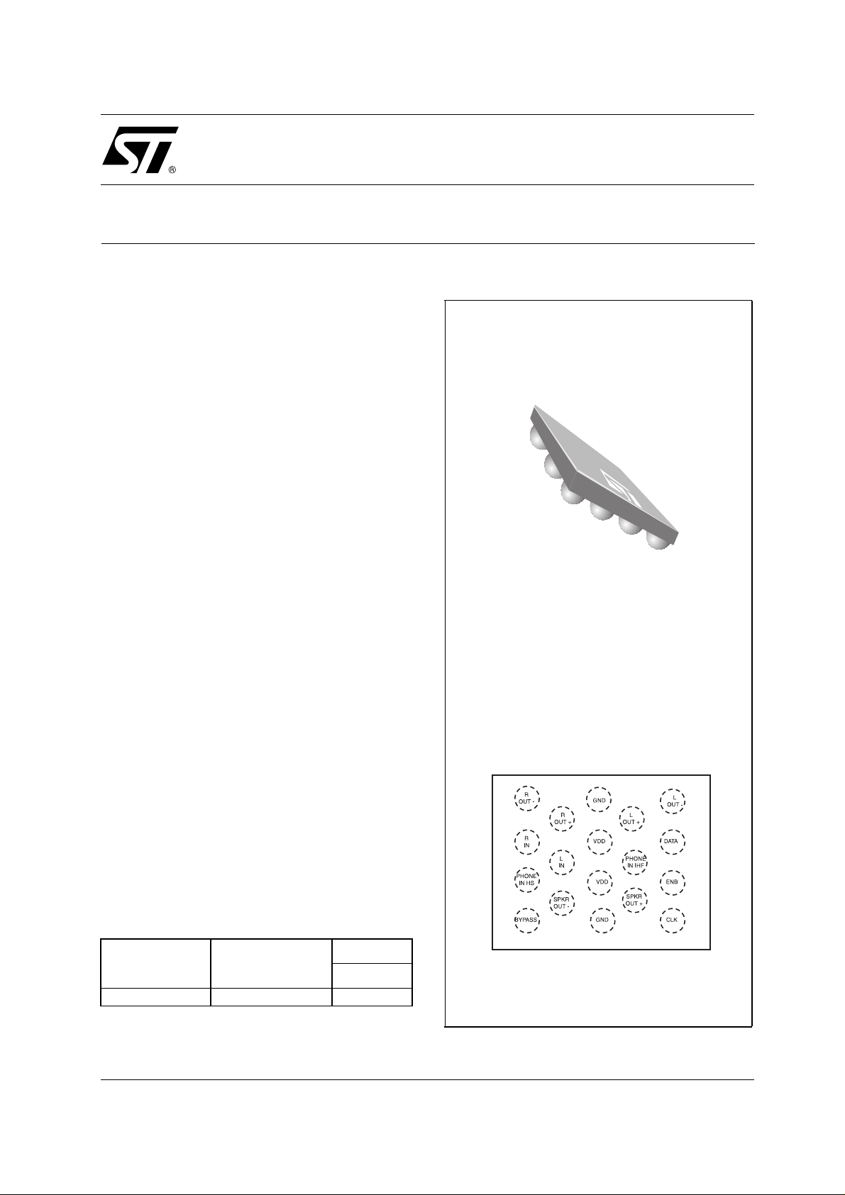
PIN CONNECTIONS (top view)
TS4855IJT - Flip Chip
Ω
Pin Out (top view)
This device features a 32-step digital volume
control and 8 different output selections. The
digital volume and output modes are controlled
through a three-digit SPI interface bus.
APPLICATIONS
• Mobile Phones
ORDER CODE
Part Number
TS4855IJT -40, +85°C
J = Flip Chip Package - only available in Tape & Reel (JT))
April 2003
Temperature
Range
Package
J
•
1/27
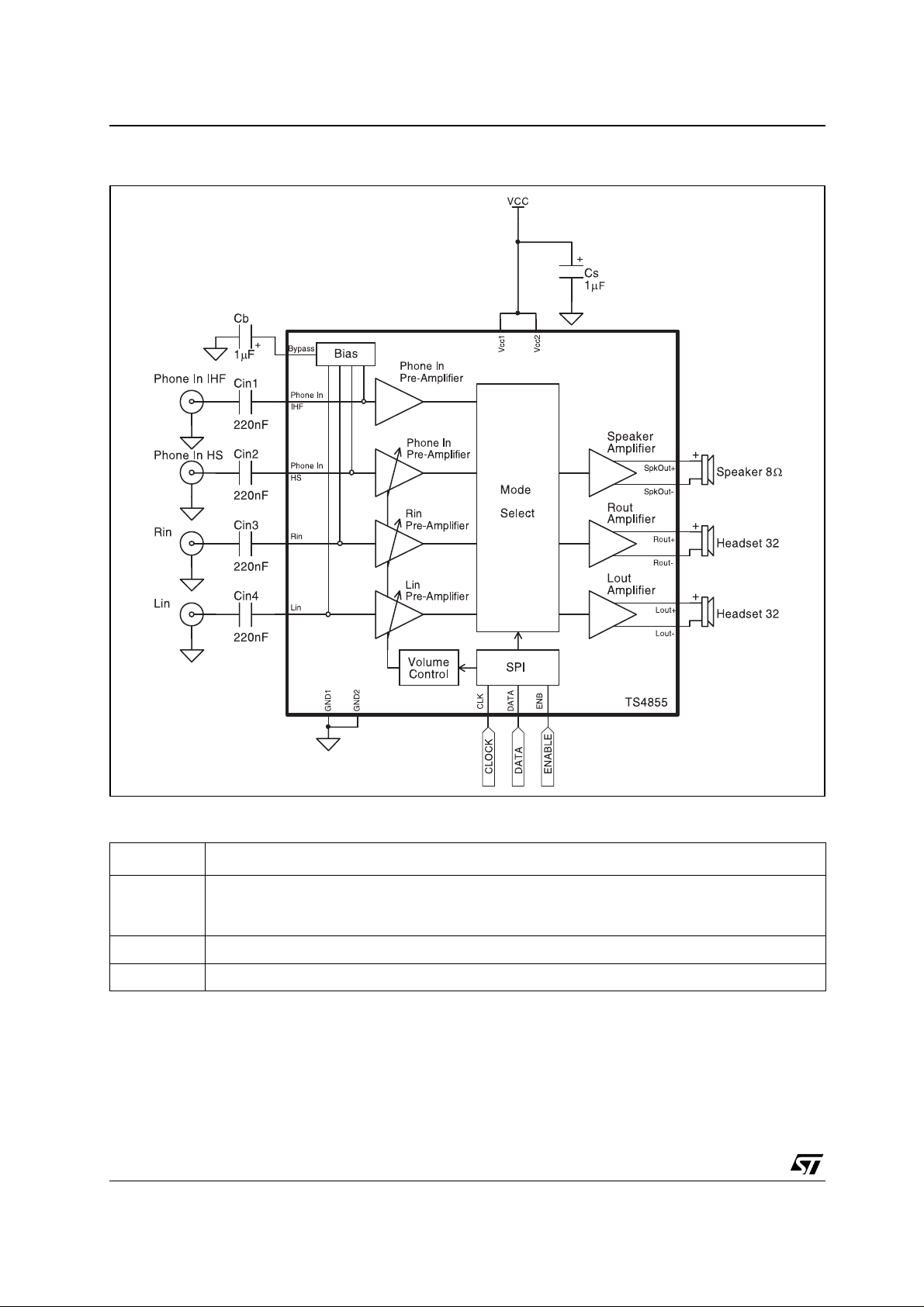
TS4855 Application Information for a Typical A pp lication
1 APPLICATION INFORMATION FOR A TYPICAL APPLICATION
External component descriptions
Component Functional Description
This is the input coupling capacitor. It blocks the DC voltage at, and couples the input signal to the
amplifier’s input terminals. Cin also creates a highpass filter with the internal input impedance Zin at
Fc = 1 / (2
This is the Supply Bypass capacitor. It provides power supply filtering.
This is the Bypass pin capacitor. It provides half-supply filtering.
π x Zin x Cin).
2/27
C
in
C
s
C
B
SPI Bus Interface TS4855
2 SPI BUS INTER FACE
2.1 Pin Descriptions
Pin Functional Description
DATA This is the serial data input pin
CLK This is the clock input pin
ENB This is the SPI enable pin active at high level
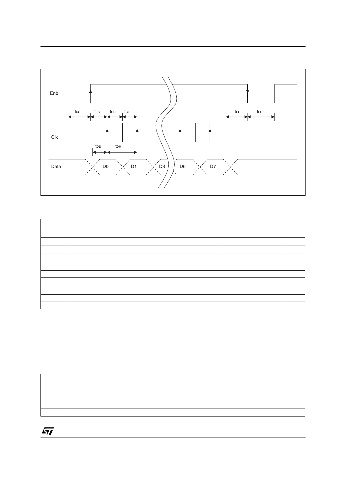
2.2 SPI Operation Description
The serial data bits are organized into a field
containing 8 bits of data as shown in
DATA 0 to DATA 2 bits determine the output
mode of the TS4855 as shown in
DATA 3 to DATA 7 bits determine the gain level
setting as illustrated by
Table 3
transfer, the data bits are written to the DATA pin
with the least significant bit (LSB) first. All serial
data are sampled at the rising edge of the CLK
signal. Once all the dat a bi ts h ave been sampled,
ENB transitions from logic-high to logic low to
complete the SPI sequence. All 8 bits must be
received before any data latch can occur. Any
excess CLK and DATA tran sitio ns w ill b e igno red
after the height rising clock edge has occurred.
For any data sequence longer than 8 bits, only the
Table 1
Table 2
. The
. The
. For each SPI
first 8 bits will get loaded into the shift register and
the rest of the bits will be disregarded.
Table 1 : Bit Allocation
DATA MODE S
LSB DATA 0 Mode 1
DATA 1 Mode 2
DATA 2 Mode 3
DATA 3 gain 1
DATA 4 gain 2
DATA 5 gain 3
DATA 6 gain 4
MSB DATA 7 gain 5
Table 2: Output Mode Selection
Output
Mode #
0 0 0 0 SD SD SD
10 0 1
2 0 1 0 MUTE
30 1 1
4 1 0 0 MUTE
51 0 1
6 1 1 0 MUTE
71 1 1
DATA 2 DATA 1 DATA 0
SPKR
+12dBxP
+12dBxP
+12dBxP
+12dBxP
out
IHF
IHF
IHF
IHF
R
out
SD SD
G1xP
HS
G1xP
HS
G2xR
in
G2xR
in
G2xR
G2xR
HS
+
in
in
G1xP
G1xPHS+
L
out
G1xP
HS
G1xP
HS
G2xL
in
G2xL
in
G1xPHS+
G2xL
in
G1xPHS+
G2xL
in
(SD = Shut Down Mode,
PHS = Non Filtered Phone In HS, P
= External High Pass Filtered Phone In IHF)
IHF
3/27

TS4855 SPI Bus Interface
Table 3: Gain Control Settings
G2: Gain (dB) G1: Gain (dB) DATA 7 DATA 6 DATA 5 DATA 4 DATA 3
-34.5 -40.5 0 0 0 0 0
-33.0 -39.0 0 0 0 0 1
-31.5 -37.5 0 0 0 1 0
-30.0 -36.0 0 0 0 1 1
-28.5 -34.5 0 0 1 0 0
-27.0 -33.0 0 0 1 0 1
-25.5 -31.5 0 0 1 1 0
-24.0 -30.0 0 0 1 1 1
-22.5 -28.5 0 1 0 0 0
-21.0 -27.0 0 1 0 0 1
-19.5 -25.5 0 1 0 1 0
-18.0 -24.0 0 1 0 1 1
-16.5 -22.5 0 1 1 0 0
-15.0 -21.0 0 1 1 0 1
-13.5 -19.5 0 1 1 1 0
-12.0 -18.0 0 1 1 1 1
-10.5 -16.5 1 0 0 0 0
-9.0 -15.0 1 0 0 0 1
-7.5 -13.5 1 0 0 1 0
-6.0 -12.0 1 0 0 1 1
-4.5 -10.5 1 0 1 0 0
-3.0 -9.0 1 0 1 0 1
-1.5 -7.5 1 0 1 1 0
0.0 -6.0 1 0 1 1 1
1.5 -4.5 1 1 0 0 0
3.0 -3.0 1 1 0 0 1
4.5 -1.5 1 1 0 1 0
6.0 0.0 1 1 0 1 1
7.5 1.5 1 1 1 0 0
9.0 3.0 1 1 1 0 1
10.5 4.5 1 1 1 1 0
12.0 6.0 1 1 1 1 1
4/27
Absolute Maximum Ratings TS4855
2.3 SPI Timing Diagram
3 ABSOLUTE MAXIMUM RATINGS
Symbol Parameter Value Unit
V
CC Supply voltage
T
T
R
Operating Free Air Temperature Range -40 to + 85 °C
oper
Storage Temperature -65 to +150 °C
stg
T
Maximum Junction Temperature 150 °C
j
Flip Chip Thermal Resistance Junction to Ambient
thja
1
2
6V
166 °C/W
Pd Power Dissipation Internally Limited
ESD
ESD
Human Body Model
Machine Model
4
3
2kV
100 V
Latch-up Immunity 200 mA
Lead Temperature (solde ring, 10sec ) 250 °C
1) All voltage values are measured with respect to the ground pin.
2) Device is protected in case of over temperature by a thermal shutdown active @ 150°C typ.
3) Human body model, 100pF discharged through a 1.5kΩ resistor into pin of device.
4) This is a minimum Value. Machine model ESD, a 200pF cap is charged to the specified voltage, then discharged directly into the IC with no external
series resistor (internal resistor < 5Ω), into pin to pin of device.
5.) All PSRR data limits are guaranteed by evaluation tests.
4 OPERATING CONDITIONS
Symbol Parameter Value Unit
V
V
V
Rin/VLin
T
Supply Voltage 3 to 5 V
CC
to VCC
Maximum Phone In Input Voltage
phin
Maximum Rin & Lin Input Voltage
Thermal Shutdown Temperature 150 °C
SD
G
ND
to V
G
ND
CC
V
V
5/27
TS4855 Electrical Characteristics
5 ELECTRICAL CHARACTERISTICS
Table 4: Electrical characteristics at VCC = +5 .0 V, GND = 0 V, Tamb = 25°C
(unless otherwise specified)
Symbol Parameter Min. Typ. Max. Unit
I
CC
I
STANDBY
Supply Current, all gain @ max settings
Output Mode 1, Vin = 0 V, no load
Output Mode 1, Vin = 0 V, loaded (8Ω)
Output Mode 2,3,4,5,6,7 Vin = 0 V, no loads
Output mode 2,3,4,5,6,7 Vin = 0 V, loaded (8Ω, 32Ω)
Standby Current
4.0
5.5
8.0
10
11
12
mA
8
9
µA
Output Mode 0 0.1 2
Voo Output Offset Voltage (differential)
Output Mode 1 to 7, Vin = 0 V, no load, Speaker Out
Output Mode 2 to 7 Vin = 0 V, no loads, Headset Out
5
5
20
40
mV
Vil “Logic low” input Voltage 0 0.4 V
Vih “Logic high” input Voltage 1.4 5 V
Po Output Pow e r
SPKR
R
out
, RL = 8Ω, THD+N = 1%, f = 1 kHz
out
& L
, RL = 32Ω, THD+N = 0.5%, f = 1 kHz
out
800701100
100
mW
THD + N Total Harmonic Distortion + Noise
R
& L
out
SPKR
R
out
SPKR
, Po = 70 mW, f = 1 kHz, RL = 32Ω
out
, Po = 800 mW, f = 1 kHz, RL = 8Ω
out
& L
, Po=50mW, 20Hz<f< 20kHz, RL=32Ω
out
, Po=400mW, 20Hz<f<20kHz, RL=8Ω
out
SNR S ignal To Noise Ratio
0.5
1
0.5
0.5
80 dB
A-Weighted, f = 1 k Hz
5)
PSRR
Power Supply Rejection Ratio
SPKR
;V ri ppl e= 200 mV Vpp, F= 217 Hz, In pu t Terminated 50Ω
out
Gain (BTL) = 12 dB, Output mode 1,3,5,7
R
& L
out
;Vripple = 200 mV Vpp, F = 217 Hz, Input T erminated 50Ω
out
Maximum gain setting, Output mode 2,3
& L
R
out
;Vripple = 200 mV Vpp, F = 217 Hz, Input T erminated 50Ω
out
Maximum gain setting, Output mode 4,5
R
& L
out
;Vripple = 200 mV Vpp, F = 217 Hz, Input T erminated 50Ω
out
Maximum gain setting, Output mode 6,7
58
52
50
46
61
55
53
49
dB
%
G2 Digital Gain Range (Rin & Lin) to R
out
G1 Digital Gain Range (Phone In HS) to R
Digital Gain Stepsize 1.5 dB
Stepsize Error ± 0.6 dB
6/27
, L
out
out
, L
out
-34. 5 12 dB
-40.5 6 dB

Electrical Characteristics TS4855
Table 4: Electrical characteristics at VCC = +5 .0 V, GND = 0 V, Tamb = 25°C
(unless otherwise specified)
Symbol Parameter Min. Typ. Max. Unit
Phone In Volume
BTL maximum GAIN from Phone In HS to R
BTL minimum GAIN from Phone In HS to R
Phone In Volume
BTL maximum gain from Rin, Lin to R
BTL minimum gain from Rin, Lin to R
out
out
, L
, L
out
Phone In Volume
BTL gain from Phone In IHF to SPKR
out
out
out
out
, L
, L
out
out
5.4
-41. 16-40.5
11.4
-35. 112-34.5
6.6
-39.9
12.6
-33.9
11.4 12 12.6 dB
dB
dB
Zin Phone In IHF Input Impedance 16 20 24 kΩ
Zin Phone In HS, Rin & Lin Input Impedance, All Gain setting 42.5 50 57.5 kΩ
tes Enable Step up Time - ENB 20 ns
teh Enable Hold Time - ENB 20 ns
tel Enable Low Time - ENB 30 ns
tds Data Setup Time- DATA 20 ns
tdh Data Hold T ime - DATA 20 ns
tcs Clock Setup time - CLK 20 ns
tch Clock Logic High Time - CLK 50 ns
tcl Clock Logic Low Time - CLK 50 ns
fclk Clock Frequency - CLK DC 10 MHz
T able 5: Electrical characteristics at VCC = +3.0 V, GND = 0 V, Tamb = 25°C
(unless otherwise specified)
Symbol Parameter Min. Typ. Max. Unit
I
CC
I
STANDBY
Supply Current, all gain @ max settings
Output Mode 1, Vin = 0 V, no load
Output Mode 1, Vin = 0 V, loaded (8Ω)
Output Mode 2,3,4,5,6,7 Vin = 0 V, no loads
Output mode 2,3,4,5,6,7 Vin = 0 V , loaded (8Ω, 32Ω)
Standby Current
3.5
4.5
7.5
9
10
11
Output Mode 0 0.1 2
Voo Output Offset Voltage (differential)
Output Mode 1 to 7, Vin = 0 V, no load, Speaker Out
Output Mode 2 to 7 Vin = 0 V, no loads, Headset Out
5
5
20
40
Vil “Logic low” input Vol tage 0 0.4 V
Vih “Logic high” input Voltage 1.4 3 V
mA
7
8
µA
mV
7/27
TS4855 Electrical Characteristics
T able 5: Electrical characteristics at VCC = +3.0 V, GND = 0 V, Tamb = 25°C
(unless otherwise specified)
Symbol Parameter Min. Typ. Max. Unit
Po Output Power
SPKR
R
out
, RL = 8Ω, TH D = 1 %, f = 1 kHz
out
& L
, RL = 32Ω, THD = 0.5%, f = 1 kHz
out
THD + N Total Harmonic Distortion + Noise
R
& L
out
SPKR
R
out
SPKR
, Po=20mW, f=1kHz, RL=32Ω
out
, Po = 300 mW, f = 1 kHz, RL = 8Ω
out
& L
, Po=15mW, 20Hz<f<20kHz, RL = 32Ω
out
, Po = 25 0 mW, 20 Hz < f < 20 kHz, RL = 8Ω
out
SNR Signal To Noise Ratio
A-Weighted, f = 1 kHz
5)
PSRR
Power Supply Rejection Ratio
SPKR
,Vripple= 200 mV Vpp, F = 217 Hz, Input Terminated 50Ω
out
Gain (BTL) = 12 dB, Output Mode 1,3,5,7
R
& L
out
Vri ppl e=200 mV Vpp, F= 217 Hz, Input Termi nat ed 50Ω
out
Maximum gain setting, Output Mode 2,3
R
& L
out
Vri ppl e=200 mV Vpp, F= 217 Hz, Input Termi nat ed 50Ω
out
Maximum gain setting, Out put Mode 4,5
R
& L
out
Vri ppl e=200 mV Vpp, F= 217 Hz, Input Termi nat ed 50Ω
out
Maximum gain setting, Out put Mode 6,7
G2 Digital Gain Range - Rin & Lin to R
out ,Lout
G1 Digital Gain Range - Phone In HS to R
Digital Gain stepsize 1.5 dB
30020340
25
0.5
1
0.5
0.5
80 dB
58
52
49
45
61
55
52
48
-34.5 12 dB
out ,Lout
-40.5 6 dB
mW
%
dB
Stepsize Error ± 0.6 d B
Phone In Volume
BTL maximum GAIN from Phone In HS to R
BTL minimum GAIN from Phone In HS to R
out
out
, L
, L
out
out
5.4
-41.16-40.5
6.6
-39.9
Phone In Volume
BTL maximum gain from Rin, Lin to R
BTL minimum gain from Rin, Lin to R
out
out
, L
, L
out
out
11.4
-35.112-34.5
12.6
-33.9
Phone In Volume
BTL gain from Phone In IHF to SPKR
out
11.4 12 12 .6
Zin Phone In IHF Input Impedanc e, all gains setting 16 20 24 kΩ
Zin Phone In HS, Rin & Lin Input Impedance, all gains setting 42.5 50 57.5 kΩ
tes Enable Step up Time - ENB 20 ns
teh Enable Hold Time - ENB 20 ns
tel Enable Low Time - ENB 30 ns
8/27
dB
dB
dB

Electrical Characteristics TS4855
T able 5: Electrical characteristics at VCC = +3.0 V, GND = 0 V, Tamb = 25°C
(unless otherwise specified)
Symbol Parameter Min. Typ. Max. Unit
tds Data Setup Time- DAT A 20 ns
tdh Data Hold Time - DA TA 20 ns
tcs Clock Setup time - CLK 20 ns
tch Clock Logic High Time - CLK 50 ns
tcl Clock Logic Low Time - CLK 50 ns
fclk Clock Frequency - CLK DC 10 MHz
Index of Graphics
Description Figure Page
THD + N vs. Output Power
THD + N vs. Frequency
Output Power vs. Power Su ppl y Voltage
Output Power vs. Load Resistor
PSRR vs. Frequency
Mute Attenuation vs. Frequency
Frequency Response
-3 dB Lower Cut Off Frequency vs. Input Capacitor
-3 dB Lower Cut Off Frequency vs. Gain Setting
Power Derating Curves
Signal to Noise Ratio vs. Power Supply Voltage
Current Consumption vs. Power Supply Voltage
Power Dissipation vs. Output Power
Note:
In the grap hs that follow, the abbreviation s Spkout = Speake r Output, and HDout = Headphone Output are
used.
Figures 1
Figures 12
Figures 19
Figures 23
Figures 27
Figures 36
Figures 39
Figures 43
Figures 52
to
11 page 10
to
18 page 11
to
22 page 13
to
26 page 13
to
34 page 14
Figure 35 page 15
to
38 page 15
to
40 page 16
Figure 39 page 16
Figure 42 page 16
to
50 page 17
Figure 51 page 18
to
55 page 18
to
to
to
to
to
to
to
page 11
page 12
page 14
page 15
page 16
page 18
page 19
9/27
 Loading...