

SGS Thomson Microelectronics TS4851IJT, TS4851 Datasheet
TS4851
MONO 1 W SPEAKER AND STEREO 160 mW HEADSET
BTL DRIVERS WITH DIGITAL VOLUME CONTROL
■ Operating from VCC=3V to 5.5V
■ Rail to rail input/output
■ Speaker driver with 1 W output @
Vcc=5V, THD+N=1%, F=1kHz, 8Ω load
■ Headset drivers with 160 mW output @
Vcc = 5 V, THD+N = 1%, F = 1 kHz, 32 Ω load
■ Headset output is 30 m W i n stereo @
Vcc=3V
■ THD+N < 0.5% Max @ 20 mW into 32
Ω
BTL, 50 Hz < Frequency < 20 kHz
■ 32-step di gi t al vol um e control from -
34.5 dB to +12 dB
■ +6 dB power up volume and full standby
■ 8 diffe rent output mod es
■ Pop & click reduction circuitry
■ Low shutdown current (< 100 nA)
■ Thermal shutdown pr otection
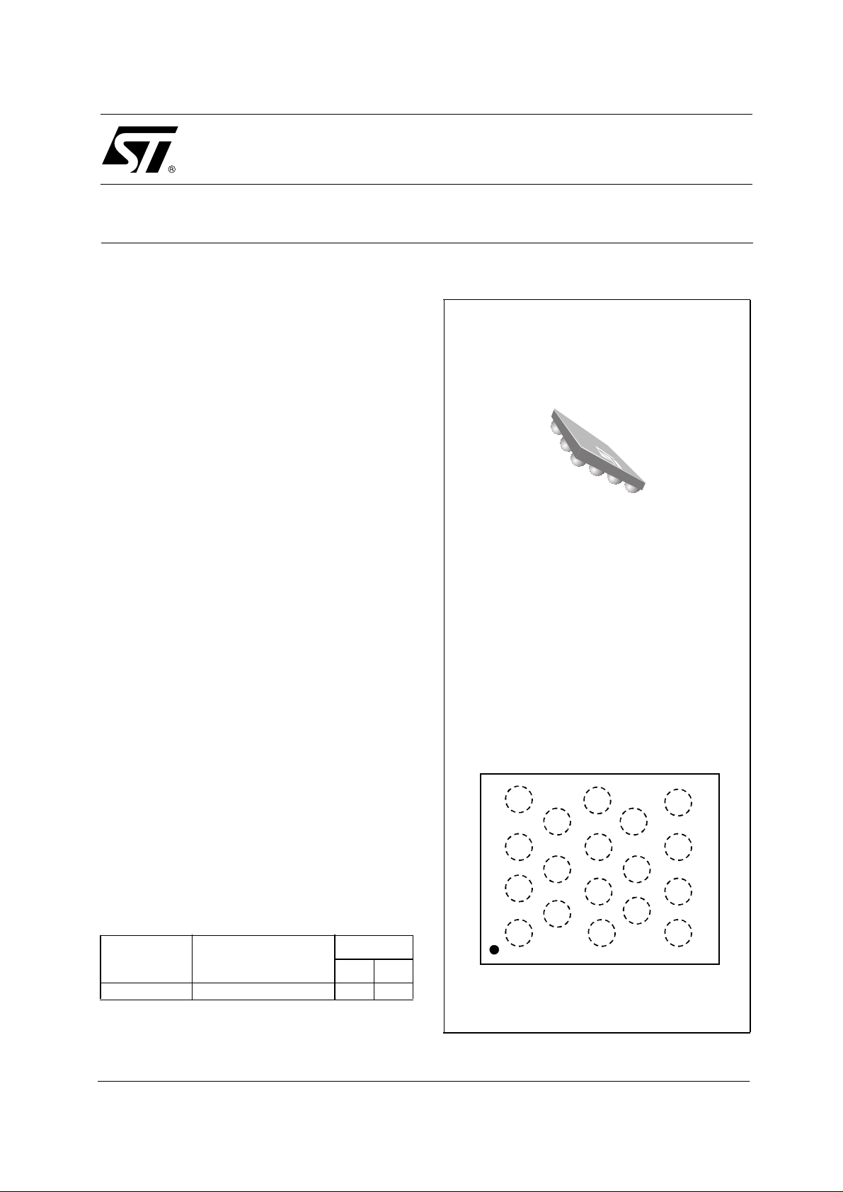
■ Flip-chip package 18 x 300 µm bumps
DESCRIPTION
The TS4851 is a low power audio amplifier that
can drive either b oth a mon o speake r or a ste reo
headset. To the speaker, it can deliver 400 mW
(typ.) of continuous RMS output power into an 8
load with a 1% THD+N value. To the headset
driver, the amplifier can deliver 30 m W (typ.) per
channel of continuous average power into a
stereo 32
@ 3.3 V.
Ω bridged-tied load with 0.5% THD+N
PIN CONNECTIONS (top view)
TS485IJT - Flip Chip
Ω
Pin Out (top view)
This device features a 32-step digital volume
control and 8 different output selections. The
digital volume and output modes are controlled
through a three-digit SPI interface bus.
APPLICATIONS
■ Mobile Phones
ORDER CODE
R
R
OUT<
OUT<
-
-
R
R
IN
IN
PHONE
PHONE
IN
IN
BYPASS
BYPASS
OUT +
OUT +
IN
IN
SPKR
SPKR
OUT+
OUT+
GND
GND
R
R
VCC DATA
VCC DATA
L
L
VCC
VCC
GND CLK
GND CLK
L
L
OUT +
OUT +
SPKR
SPKR
OUT -
OUT -
L
L
OUT -
OUT -
NC
NC
ENB
ENB
Package
Part Number Temperature Range
J
TS4851IJT -40, +85°C
J = Flip Chip Package - only available in Tape & Reel (JT))
•
April 2003 Revision B 1/26
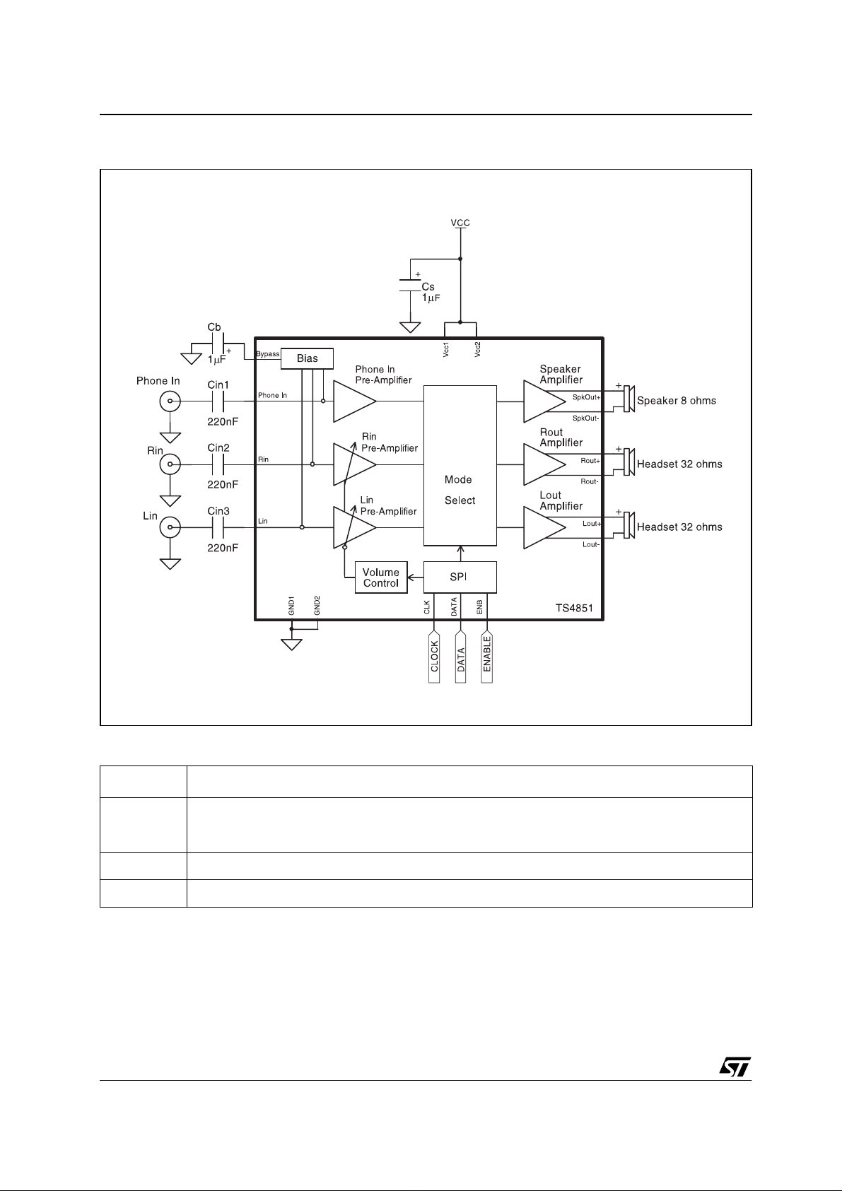
TS4851 Application Information for a Typical A pp lication
1 APPLICATION INFORMATION FOR A TYPICAL APPLICATION
External component descriptions
Component Functional Description
This is the input coupling capacitor. It blocks the DC voltage at, and couples the input signal to the
amplifier’s input terminals. Cin also creates a highpass filter with the internal input impedance Zin at Fc
=1/ (2
πi x Zin x Cin).
This is the Supply Bypass capacitor. It provides power supply filtering.
This is the Bypass pin capacitor. It provides half-supply filtering.
2/26
C
in
C
s
C
B
SPI Bus Interface TS4851
2 SPI BUS INTER FACE
2.1 Pin descriptions
Pin Functional Description
DATA This is the serial data input pin.
CLK This is the clock input pin.
ENB This is the SPI enable pin active at high level.
2.2 Description of SPI operation
The serial data bits are organized into a field
containing 8 bits of data as shown in
Table 1
. The
first 8 bits will get loaded into the shift register and
the rest of the bits will be disregarded.
Ta ble 1: Bit Allocatio n
DATA 0 to DATA 2 bits determine the output
mode of the TS4851 as shown in
Table 2
. The
DATA 3 to DATA 7 bits determine the gain level
setting as illustrated by
Table 3
. For each SPI
transfer, the data bits are written to the DATA pin
with the least significant bit (LSB) first. All serial
data are sampled at the rising edge of the CLK
signal. Once all the dat a bi ts h ave been sampled,
ENB transitions from logic-high to logic low to
complete the SPI sequence. All 8 bits must be
LSB DATA 0 Mode 1
DA TA MODES
DATA 1 Mode 2
DATA 2 Mode 3
DATA 3 gain 1
DATA 4 gain 2
DATA 5 gain 3
received before any data latch can occur. Any
excess CLK and DATA tran sitio ns w ill b e igno red
after the height rising clock edge has occurred.
MSB DATA 7 gain 5
DATA 6 gain 4
For any data sequence longer than 8 bits, only the
Table 2: Outpu t mode selection: G from -34.5 dB to +12 dB (by steps of 1.5 dB)
Output
Mode #
0 0 0 0 SD SD SD
1 0 0 1 6dBxP SD SD
2 0 1 0 SD 0dBxP 0dBxP
3 0 1 1 Gx(R+L) SD SD
4 1 0 0 SD GxR GxL
5 1 0 1 Gx(R+L)
6 1 1 0 SD GxR+0dBxP GxL+0dBxP
7 1 1 1 6dBxP GxR+0dBxP GxL+0dBxP
DATA 2 DATA 1 DATA 0
SPKERout
+6dBxP
1
Rout Lout
SD SD
1) SD = Shutd own Mode, P = Phone in Input, R = Rin input and L = Li n i nput
3/26
TS4851 SPI Bus Interface
Table 3: Volume Control Settings
K :
Gain (dB) DATA 7 DATA 6 DATA 5 DATA 4 DATA 3
-34.5 0 0 0 0 0
-33.0 0 0 0 0 1
-31.5 0 0 0 1 0
-30.0 0 0 0 1 1
-28.5 0 0 1 0 0
-27.0 0 0 1 0 1
-25.5 0 0 1 1 0
-24.0 0 0 1 1 1
-22.5 0 1 0 0 0
-21.0 0 1 0 0 1
-19.5 0 1 0 1 0
-18.0 0 1 0 1 1
-16.5 0 1 1 0 0
-15.0 0 1 1 0 1
-13.5 0 1 1 1 0
-12.0 0 1 1 1 1
-10.5 1 0 0 0 0
-9.0 1 0 0 0 1
-7.5 1 0 0 1 0
-6.0 1 0 0 1 1
-4.5 1 0 1 0 0
-3.0 1 0 1 0 1
-1.5 1 0 1 1 0
0.0 10111
1.5 11000
3.0 11001
4.5 11010
6 11011
7.5 11100
9 11101
10.5 1 1 1 1 0
12 11111
4/26
SPI Bus Interface TS4851
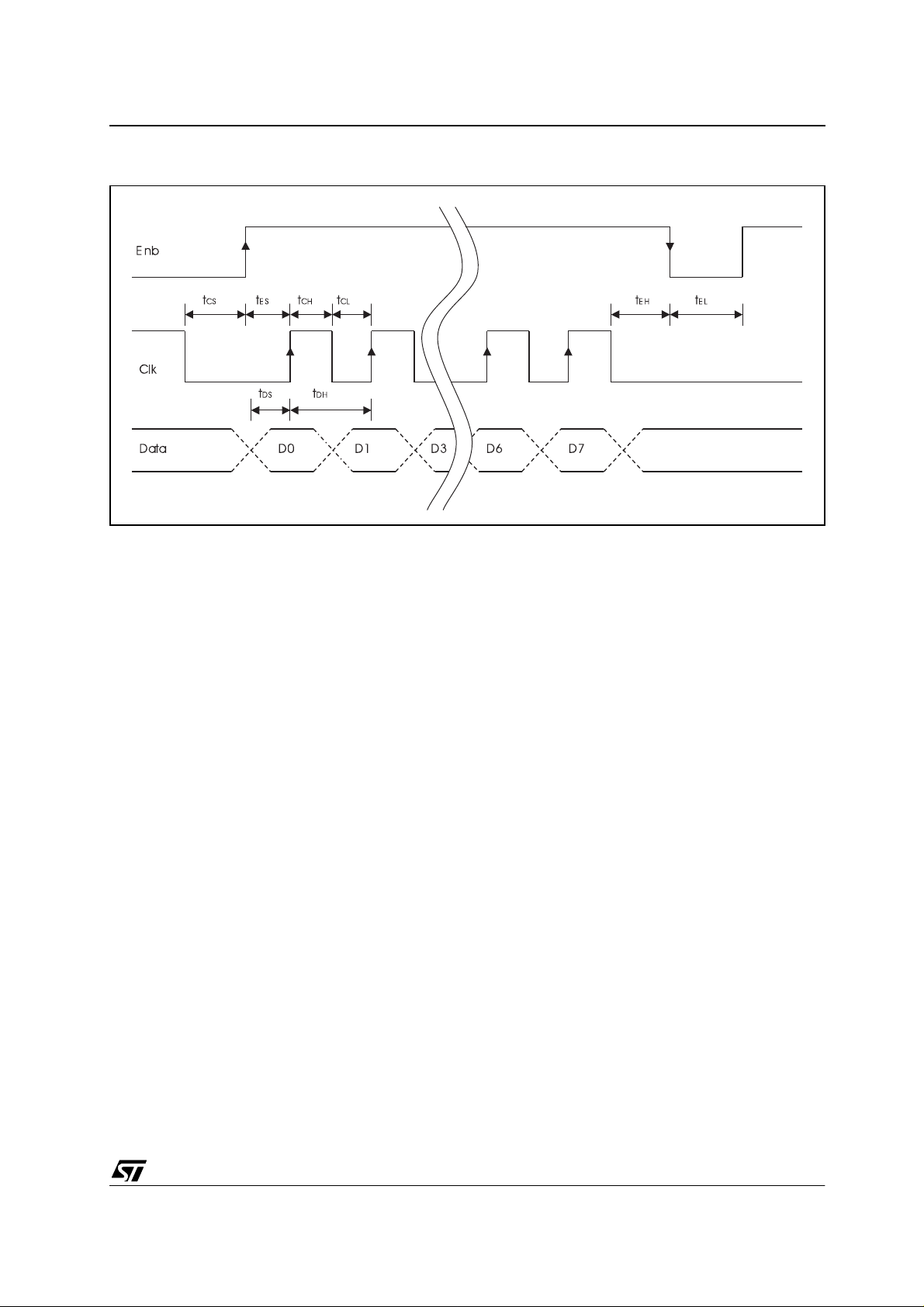
2.3 SPI Timing Diagram
5/26
TS4851 Absolute Maximum Ratings
3 ABSOLUTE MAXIMUM RATINGS
Symbol Parameter Value Un it
VCC
T
oper
T
stg
T
R
thja
Supply voltage
Operating Free Air Temperature Range -40 to + 85 °C
Storage Temperature -65 to +150 °C
Maximum Junction Temperature 150 °C
j
Flip Chip Thermal Resistance Junction to Ambient
Pd Power Dissipation Internally Limited
ESD Human Body Model 2 kV
ESD Machine Model 100 V
Latch-up Immunity 200 mA
Lead Te mpera ture (solde ring, 10se c) 250 °C
1) All volta ges values are me asured with r espect to the ground pin.
2) D evice is prote ct ed in case of over temperature by a thermal shutdown act i ve @ 150°C
1
2
6V
200 °C/W
4 OPERATING CONDITIONS
Symbol Parameter Value Unit
VCC Supply Voltage 3 to 5.5 V
V
phin
Maximum Phone In Input Voltage GND to VCC V
VRin/VLin Maximum Rin & Lin Input Voltage G
TSD Thermal Shut Down Temperature 150 °C
R
thja
1) D evice is prote ct ed in case of over temperature by a thermal shutdown act i ve @ 150°C
Flip Chip Thermal Resistance Junction to Ambient
1
to V
ND
CC
90 °C/W
V
6/26
Electrical Characteristics TS4851
5 ELECTRICAL CHARACTERISTICS
Table 4: Electrical characteristics at VCC = +5 V, GND = 0 V, Tamb = 25°C (unless otherwise
specified)
Symbol Parameter Min. Typ. Max. Unit
I
CC
I
STANDBY
Supply Current
Output Mode 7, Vin = 0 V, no load
All other output modes, Vin = 0 V, no load
Standby Current
8
4.5
11
mA
6.5
µA
Output Mode 0 0.1 2
Voo Output Offset Voltage (differential)
mV
Vin = 0 V 5 50
Vil “Logic low” input Voltage 0 0.4 V
Vih “Logic high” input Voltage 1.4 5 V
Po Output Power
SPKERout, RL = 8
Rout & Lout, RL = 32
THD = 1%, F = 1 kHz
Ω,
THD = 0 .5%, F = 1 kHz
Ω,
THD + N Total Harmonic Distortion + Noise
Rout & Lout, Po = 80 mW, F = 1 kHz, RL = 32
SPKERout, Po = 800 mW, F = 1 kHz, RL = 8
Rout & Lout, Po = 50 mW, 20 Hz < F < 20 kHz, RL = 32
SPKERout, Po = 40 mW, 20 Hz < F < 20 kHz, RL = 8
800801000
120
Ω
Ω
Ω
Ω
0.5
1
0.5
1
mW
%
SNR Signal To Noise Ratio (A-Weighted) 90 dB
1
PSRR
Power Supply Rejection Ratio (Output Mode = 2)
Vripple = 200 mV Vpp, F = 217 Hz, Input Floating
Vripple = 200 mV Vpp, F = 217 Hz, Input Terminated 10
G Digital Gain Range - Rin & Lin
2
dB
61
Ω
62
dB
no load -34.5 +12
Digital gain stepsize 1.5 dB
Stepsize
G ≥ -22.5 dB
G < -22.5 dB
-0.5
-1
+0.5
+1
Phone In Gain, no load
BTL gain from Phone In to SPKERout
BTL gain from Phone In to Rout & Lout
6
0
Zin Phone In Input Impedance 15 20 25 k
Zin Rin & Lin Input Impedance (all gain setting) 37.5 50 62.5 k
dB
dB
Ω
Ω
tes Enable Stepup Time - ENB 20 ns
teh Enable Hold Time - ENB 20 ns
tel Enable Low Time - ENB 30 ns
tds Data Setup Time- DATA 20 ns
tdh Data Hold Time - DATA 20 ns
tcs Clock Setup time - CLK 20 ns
tch Clock Logic High Time - CLK 50 ns
tcl Clock Logic Low Time - CLK 50 ns
fclk Clock Frequency - CLK DC 10 MHz
1) All PSRR data limits are guaranted by evaluation desgin test.
2) Dynamic measurements [20 x log(rms(Vout)/rms (Vripple)] . V ri pple is the sup eri m posed sinus si gnal to Vcc @ F = 217 Hz
7/26
TS4851 Electrical Characteristics
Table 5: El ectri cal character istics at VCC = +3.0V, GND = 0V, Tamb = 25°C (unless otherwise
specified)
Symbol Parameter Min. Ty p. Max. Unit
I
CC
I
STANDBY
Voo Output Offset Voltage (differential)
Supply Current
Output Mode 7, Vin = 0 V,no load
All other output modes, Vin = 0 V,no load
7.5
4.5
6.5
Standby Current
Output Mode 0 0.1 2
mA
10
µA
mV
Vin = 0 V 5 50
Vil “Logic low” input Voltage 0 0.4 V
Vih “Logic high” input Voltage 1.4 5 V
Po Output Power
SPKERout, RL = 8
Rout & Lout, RL = 32
THD = 1%, F = 1 kHz
Ω,
THD = 0.5%, F = 1 kHz
Ω,
THD + N Total Harmonic Distortion + Noise
Rout & Lout, Po = 20 mW, F = 1 kHz, RL = 32
SPKERout, Po = 300 mW, F = 1 kHz, RL = 8
Rout & Lout, Po = 15 mW, 20 Hz < F < 20 kHz, RL = 32
SPKERout, Po = 250 mW, 20 Hz < F < 20 kHz, RL = 8
300
20
Ω
Ω
Ω
Ω
340
30
0.5
1
0.5
1
mW
%
SNR Signal To Noise Ratio (A-Weighted) 86 dB
1
PSRR
Power Supply Rejection Ratio (Output Mode = 2)
Vripple = 200 mV Vpp, F = 217 Hz, Input Floating
Vripple = 200 mV Vpp, F = 217 Hz, Input Terminated 10
G Digital Gain Range - Rin & Lin
2
dB
61
Ω
62
dB
no load -34.5 - +12
Digital gain stepsize 1.5 dB
Zin
Zin
Stepsize error
G ≥ -22.5 dB
G < -22.5 dB
Phone In Gain, no load
BTL gain from Phone In to SPKERout
BTL gain from Phone In to Rout & Lout
Phone In Input Impedance
1
Rin & Lin Input Impedance (All Gain Setting)
-0.5
-1
+0.5
+1
6
0
15 20 25 k
1
37.5 50 62.5 k
dB
dB
tes Enable Stepup Time - ENB 20 ns
teh Enable Hold Time - ENB 20 ns
tel Enable Low Time - ENB 30 ns
tds Data Setup Time- DATA 20 ns
tdh Data Hold Time - DATA 20 ns
tcs Clock Setup time - CLK 20 ns
tch Clock Logic High Time - CLK 50 ns
tcl Clock Logic Low Time - CLK 50 ns
fclk Clock Frequency - CLK DC 10 MHz
Ω
Ω
1) All PSRR data limits are guaranted by evaluation desgin test.
2) Dynamic measurements [20 x log(rms(Vout)/rms (Vripple)] . V ri pple is the sup eri m posed sinus si gnal to Vcc @ F = 217 Hz.
8/26
 Loading...