

TS461
TS462
TS464
OUTPUT RAIL TO RAIL
OPERATIONALAMPLIFIERS
August 1999
.
HIGHDYNAMIC FEATURES
.
LARGEOUTPUT SWING
(±2.4V @ V
CC
= ±2.5V)
.
LOW NOISE LEVEL: 4nV/√√Hz
.
LOW DISTORTION : 0.003%
.
OPERATINGRANGE : 2.7V to 12V
.
AVAILABLEIN SOT23-5 MICROPACKAGE
DESCRIPTION
The TS46xisoperationalamplifiersabletooperate
with voltages as low as ±1.35V and to reach a
minimumof ±2Vpp of output swing when supplied
with ±2.5V.
This deviceis well suited for every kind of portable
and battery-supplied equipment where low noise
and low distortionare key.
The TS461/2/4are a cost-attractive access to the
range of the Rail to Rail Op-Ampsfrom
STMicroelectonics.
APPLICATIONS
.
Soundcards
.
PDA
.
CDplayers
.
Recordingequipments
.
Multimedia
.
Microphone preamplifier
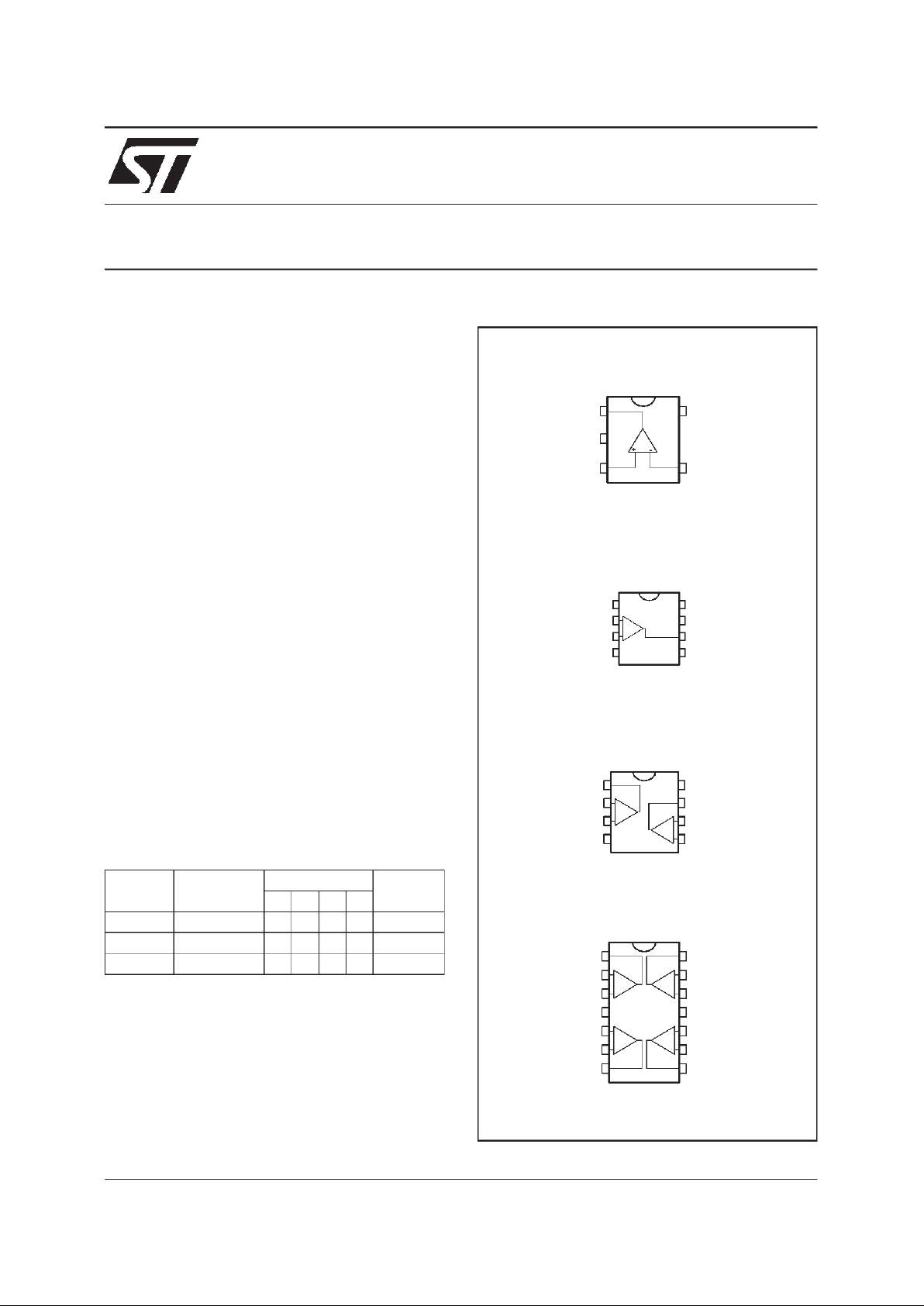
PIN CONNECTIONS (top view)
ORDER CODES
Part
Number
Temperature
Range
Package
SOT23
Marking
NDPL
TS461C -20, +70
o
C ••K105
TS462C -20, +70
o
C •••
TS464C -20, +70
o
C •••
1
2
3
4
5
6
7
8
-
+
Inverting Input 1
N.C.
Non-inve rting Inpu t 1
V
DD
V
CC
Output 2
N.C.
N.C.
TS461CD
1
2
3
4
5
Inverting input
Non-inverting input
Output
V
DD
V
CC
TS461CLT
1
2
3
45
6
7
8
-
+
-
+
Inverting Inp ut 1
Output 1
Non-inverting Inp ut 1
V
DD
V
CC
Output 2
Inverting Input 2
Non-inverting Input2
TS462CN-TS462CD-TS462CPT
Inve rting Input 2
Non-inverting Input 2
Non-inverting Input 1
DD
V
1
2
3
4
8
5
6
7
9
10
11
12
13
14
CC
V
Output 3
Output 4
Non-inverting Input 4
Inverting Input 4
Non-inverting Input 3
Inverting Input 3
-
+
+
-
+
-
+
Output 1
Inverting Input 1
Output 2
TS464CN-TS464CD-TS464CPT
N =Dual in Line Package (DIP)
D = Small Outline Package (SO) - also available in Tape& Reel
P = Thin Shrink SmallOutline Package (TSSOP) - only available
in Tape& Reel (PT)
L = Tiny Package (SOT23-5) - only available in Tape& Reel (LT)
1/10
ABSOLUTEMAXIMUM RATINGS
Symbol Parameter Value Unit
V
CC
Supply Voltage - note 1 12 V
V
id
Differential Input Voltage - note 2 ±V
CC
V
V
in
Input Voltage Range - note 3 -0.3 to 12.3 V
T
oper
Operating Free Air Temperature Range -20 to +70
o
C
T
stg
Storage Temperature -65 to +150
o
C
T
j
Maximum Junction Temperature 150
o
C
R
thjc
Thermal Resistance Junction to Case - note 4
SOT23-5
SO8
SO14
TSSOP8
TSSOP14
81
28
22
26
21
o
C/W
R
thja
Thermal Resistance Junction to Ambient (SOT23-5) 256
o
C/W
ESD Human Body Model 2 kV
Lead Temperature (soldering, 10sec) 260
o
C
Notes : 1. All voltages values,except differential voltage are with respect to network ground terminal.
2. Differential voltages are non-inverting input terminal with respect to the inverting input terminal.
3. The magniture of inputand outputvoltages must never exceed V
CC
+0.3V.
4. Short-circuits can cause excessive heating and destructive dissipation.
OPERATINGCONDITIONS
Symbol Parameter Value Unit
V
CC
Supply Voltage Range 2.7 to 10 V
V
icm
Common Mode Input VoltageRange VDD+ 1.15 to VCC- 1.15 V
TS461-TS461-TS464
2/10
ELECTRICALCHARACTERISTICS
V
CC
=2.5V,VDD= -2.5V, T
amb
=25oC (unlessotherwisespecified)
Symbol Parameter Min. Typ. Max. Unit
V
io
Input Offset Voltage
T
min.<Tamb<Tmax.
1
5mV
DV
io
Input Offset Voltage Drift
V
icm
= 0V, Vo=0V 5
µV/
o
C
I
io
Input Offset Current
V
icm
= 0V, Vo=0V
T
min.<Tamb<Tmax.
10 150
200
nA
I
ib
Input Bias Current
V
icm
= 0V, Vo=0V
T
min.<Tamb<Tmax.
200
200
750
1000
nA
V
icm
Common Mode Input VoltageRange -1.35 ±1.5 1.35 V
CMR Common Mode Rejection Ratio
V
icm
= ±1.35V 60 85
dB
SVR Supply Voltage RejectionRatio
V
CC
= ±2V to ±3V 60 70
dB
A
vd
Large Signal Voltage Gain RL=2kΩ 70 80 dB
V
OH
High Level Output Voltage RL=2kΩ 2 2.4 V
V
OL
Low LevelOutput Voltage RL=2kΩ -2.4 -2 V
I
CC
Supply Current, per amplifier
Unity gain - no load 2 2.8
mA
GBP Gain Bandwidth Product
f = 100kHz RL=2kΩ,CL= 100pF 8.5 10
MHz
SR Slew Rate
A
V
=1,Vin= ±1V 2.8 4
V/µs
e
n
Equivalent Input Noise Voltage
f = 100kHz
4
nV
√Hz
THD
Total Harmonic Distortion
f = 1kHz, A
V
=-1 RL= 10kΩ
0.003
%
TS461-TS462-TS464
3/10

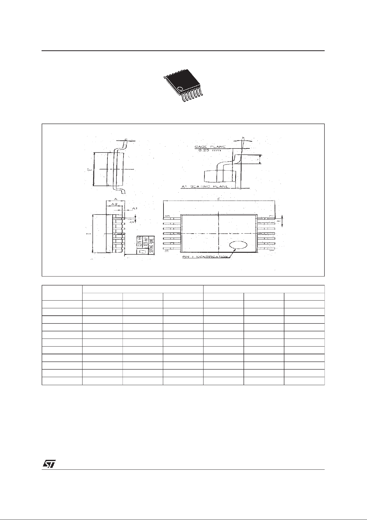
PACKAGEMECHANICALDATA
8 PINS - PLASTICDIP
Dimensions
Millimeters Inches
Min. Typ. Max. Min. Typ. Max.
A 3.32 0.131
a1 0.51 0.020
B 1.15 1.65 0.045 0.065
b 0.356 0.55 0.014 0.022
b1 0.204 0.304 0.008 0.012
D 10.92 0.430
E 7.95 9.75 0.313 0.384
e 2.54 0.100
e3 7.62 0.300
e4 7.62 0.300
F 6.6 0260
i 5.08 0.200
L 3.18 3.81 0.125 0.150
Z 1.52 0.060
TS462CN
TS461-TS461-TS464
4/10

PACKAGEMECHANICALDATA
8 PINS - PLASTICMICROPACKAGE(SO)
Dimensions
Millimeters Inches
Min. Typ. Max. Min. Typ. Max.
A 1.75 0.069
a1 0.1 0.25 0.004 0.010
a2 1.65 0.065
a3 0.65 0.85 0.026 0.033
b 0.35 0.48 0.014 0.019
b1 0.19 0.25 0.007 0.010
C 0.25 0.5 0.010 0.020
c1 45
o
(typ.)
D 4.8 5.0 0.189 0.197
E 5.8 6.2 0.228 0.244
e 1.27 0.050
e3 3.81 0.150
F 3.8 4.0 0.150 0.157
L 0.4 1.27 0.016 0.050
M 0.6 0.024
S8
o
(max.)
TS461CD-TS462CD
TS461-TS462-TS464
5/10

PACKAGEMECHANICALDATA
8 PINS - THINSHRINK SMALL OUTLINEPACKAGE(TSSOP)
Dim.
Millimeters Inches
Min. Typ. Max. Min. Typ. Max.
A 1.20 0.05
A1 0.05 0.15 0.01 0.006
A2 0.80 1.00 1.05 0.031 0.039 0.041
b 0.19 0.30 0.007 0.15
c 0.09 0.20 0.003 0.012
D 2.90 3.00 3.10 0.114 0.118 0.122
E 6.40 0.252
E1 4.30 4.40 4.50 0.169 0.173 0.177
e 0.65 0.025
k0
o
8
o
0
o
8
o
l 0.50 0.60 0.75 0.09 0.0236 0.030
TS462CPT
TS461-TS461-TS464
6/10

PACKAGEMECHANICALDATA
14 PINS- PLASTIC DIP
Dim.
Millimeters Inches
Min. Typ. Max. Min. Typ. Max.
a1 0.51 0.020
B 1.39 1.65 0.055 0.065
b 0.5 0.020
b1 0.25 0.010
D 20 0.787
E 8.5 0.335
e 2.54 0.100
e3 15.24 0.600
F 7.1 0.280
i 5.1 0.201
L 3.3 0.130
Z 1.27 2.54 0.050 0.100
TS464CN
TS461-TS462-TS464
7/10

PACKAGEMECHANICALDATA
14 PINS- PLASTIC MICROPACKAGE(SO)
Dim.
Millimeters Inches
Min. Typ. Max. Min. Typ. Max.
A 1.75 0.069
a1 0.1 0.2 0.004 0.008
a2 1.6 0.063
b 0.35 0.46 0.014 0.018
b1 0.19 0.25 0.007 0.010
C 0.5 0.020
c1 45
o
(typ.)
D 8.55 8.75 0.336 0.334
E 5.8 6.2 0.228 0.244
e 1.27 0.050
e3 7.62 0.300
F 3.8 4.0 0.150 0.157
G 4.6 5.3 0.181 0.208
L 0.5 1.27 0.020 0.050
M 0.68 0.027
S8
o
(max.)
TS464CD
TS461-TS461-TS464
8/10
PACKAGEMECHANICALDATA
14 PINS- THIN SHRINK SMALLOUTLINE PACKAGE(TSSOP)
Dim.
Millimeters Inches
Min. Typ. Max. Min. Typ. Max.
A 1.20 0.05
A1 0.05 0.15 0.01 0.006
A2 0.80 1.00 1.05 0.031 0.039 0.041
b 0.19 0.30 0.007 0.15
c 0.09 0.20 0.003 0.012
D 4.90 5.00 5.10 0.192 0.196 0.20
E 6.40 0.252
E1 4.30 4.40 4.50 0.169 0.173 0.177
e 0.65 0.025
k0
o
8
o
0
o
8
o
l 0.50 0.60 0.75 0.09 0.0236 0.030
TS464CPT
TS461-TS462-TS464
9/10

Information furnished is believed to be accurate and reliable. However, STMicroelectronics assumes no responsibility for the
consequences of use of such information nor for any infringement of patents or other rights of third parties which may result from
its use. No license is granted by implication or otherwise under any patent or patent rights of STMicroelectronics. Specifications
mentioned in this publication are subject to change without notice. This publication supersedes and replaces all information
previously supplied.STMicroelectronics products are notauthorized foruseas critical components in lifesupport devicesorsystems
without express written approval of STMicroelectronics.
The ST logo isa trademark of STMicroelectronics
1999 STMicroelectronics – Printed in Italy – All Rights Reserved
STMicroelectronics GROUP OF COMPANIES
Australia - Brazil - China - Finland - France - Germany - Hong Kong - India - Italy - Japan - Malaysia - Malta - Morocco
Singapore - Spain - Sweden - Switzerland- United Kingdom - U.S.A.
http://www.st.com
L
C
E1
A2
A
A1
b
E
D
PACKAGEMECHANICALDATA
5 PINS-TINY PACKAGE(SOT23)
Dim.
Millimeters Inches
Min. Max. Min. Max.
A 0.90 1.45 0.034 0.057
A1 0 0.15 0.006
A2 0.90 1.30 0.034 0.051
b 0.35 0.50 0.013 0.020
C 0.09 0.20 0.003 0.008
D 2.80 3.00 0.110 0.118
E 2.60 3.00 0.102 0.118
E1 1.50 1.75 0.059 0.069
L 0.10 0.60 0.003 0.024
TS461CLT
TS461-TS461-TS464
10/10
 Loading...