

TS432
1.24V ADJUSTABLE SHUNT VOLTAGE REFERENCE
■ 1.24V TYP OUTPUT VOLTAGE
■ ULTRA LOW OPERATING CURRENT :
60µA maximum at 25°C
■ HIGH PRECISION @ 25°C
+/- 1%
+/- 0.5%
■ HIGH STABILITY WHEN USED WITH
CAPACITIVE LOADS
■ INDUSTRIAL TEMPERATURE RANGE:
-40 to +85°C
■ 100ppm/°C TEM PER ATURE COEFF IC IENT
DESCRIPTION
The TS432 is an adjustable low power shunt
voltage reference providing an output voltage from
1.24V to 10V over the industrial temperature
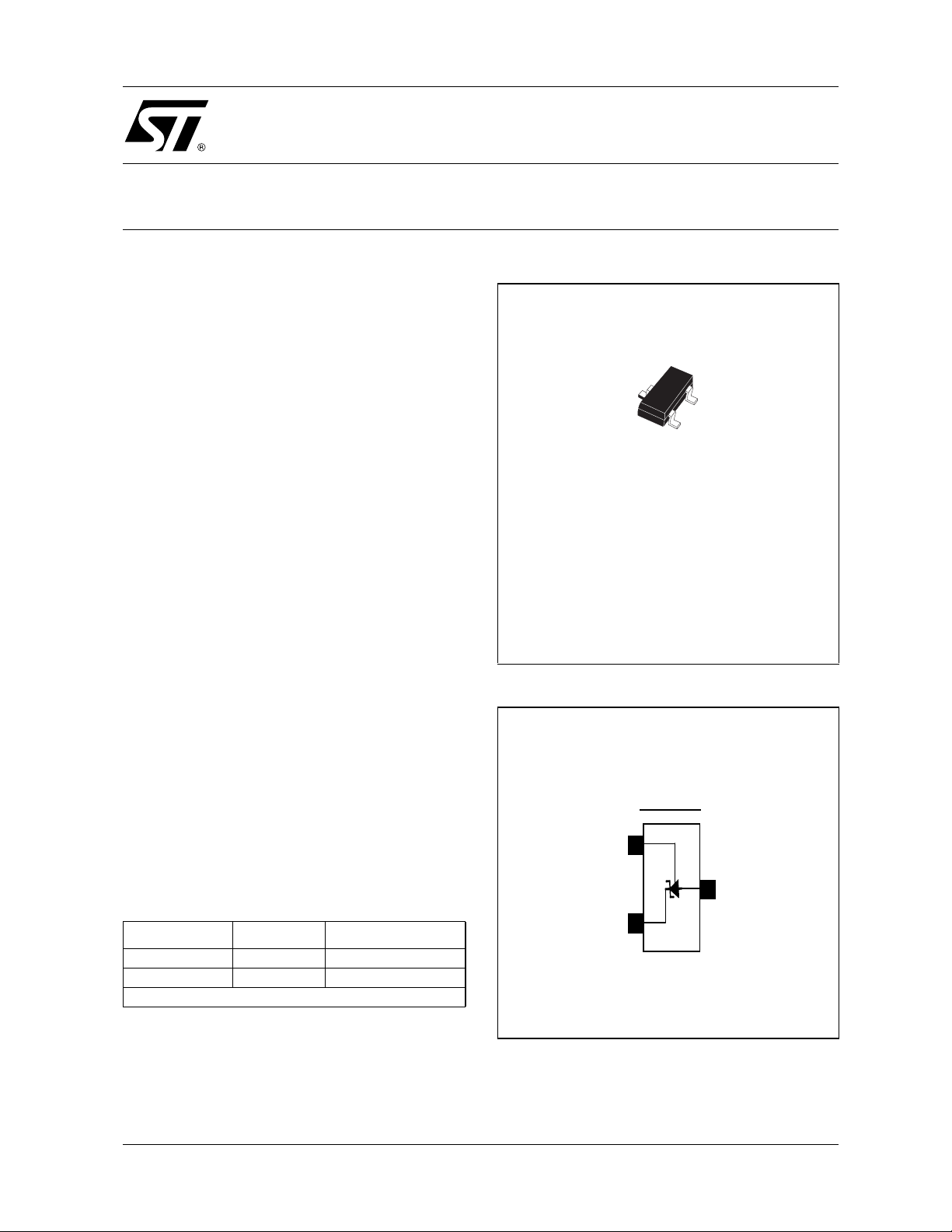
range (-40 to +85°C). Available in SOT23-3
surface mount package, it can be designed in
applications where space saving is a critical issue.
The low operating current is a key advantage for
power restricted designs. In addition, the TS432 is
very stable and can be used in a broa d range of
application conditions.
L
SOT23-3L
(Plastic Micropacka ge)
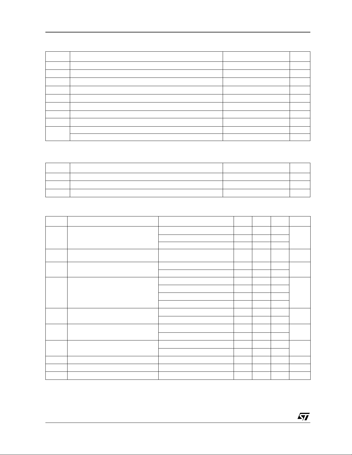
PIN CONNECTIONS (top view)
APPLICATION
■ Computers
■ Instrumentation
■ Battery chargers
■ Switch Mode Power Supply
■ Battery operated equipments
ORDER CODE
Precision SOT23-3 SOT23 Marking
1% TS432ILT L235
0.5% TS432AILT L236
Single temperature range: -40 to +85°C
LT = Tiny Package (SOT23-3) - only available in Tape & Reel (LT)
December 2002
SOT2 3-3
Ref
Reference
A
Anode
K
Cathode
1/7
TS432
ABSOLUTE MAXIMUM RATINGS
Symbol Parameter Value Unit
V
Cathode voltage 12 V
K
I
Cathode current -10 to +20 mA
K
I
R
T
LEAD
T
ESD Human Body Model (HBM) 1.5 kV
1. Pd has been ca l culated wi th T
OPERATING CONDITIONS
Symbol Parameter Value Unit
T
Reference input current -0.05 to +3 mA
REF
P
D Power dissipation
Thermal resistance junction to ambient for SOT23-3 360 °C/W
THJA
1)
SOT23-3
340 mW
Lead temperature (soldering 10 seconds) 250 °C
Storage temperature -65 to +150 °C
STG
T
Junction temperature 150 °C
J
Machine Model (MM) 150 V
= 25°C, Tj = 150°C and Rth j a = 360°C/W fo r the SOT23-3L package
amb
V
Cathode voltage 1.24 to 10 V
K
I
Cathode current 60µ to 12m A
K
Ambient temperature -40 to +85 °C
AMB
ELECTRICAL CHARACTERISTICS
T
= 25°C (unless otherwise specified)
amb
Symbol Parameter Test Condition Min. Typ. Max. Unit
I
V
REF
V
∆
REF
I
KMIN
V
∆
REF
V
∆
REF
V
∆
I
REF
I
OFF
R
KA
K
VH
E
N
Reference voltage
Reference voltage tolerance over
temperature
Minimum operating current
Reverse breakdown voltage change
with operating current range
/
Reference voltage change with output
voltage change
K
Reference input current
Off-state cathode current
Static impedance
Long term stability
Wide band noise
= 100µA, VK=V
K
REF
TS432 (1%) 1.228 1.252
TS432A (0.5%) 1.234 1.246
I
= 100µA, VK=V
K
= 25°C
T
amb
-40°C < T
I
KMIN
-40°C < T
1mA < I
-40°C < T
I
= 10mA, VK=10V to V
K
-40°C < T
=10mA, R1=10K
I
K
-40°C < T
V
REF
-40°C < T
I
∆
I
= 100µA, t = 1000hrs
K
I
= 100µA 100Hz < F < 10kHz
K
AMB
< IK < 1mA
AMB
< 12mA
K
AMB
AMB
AMB
=0, VK=10V
AMB
= 100µA to 12mA
K
REF
< +85°C
< +85°C
< +85°C
< +85°C
Ω,
< +85°C
< +85°C
REF
R2=+
∞
1.24
716mV
40 60
65
0.7 1.5
2
24
mV
6
1.8 2.5
mV/V
3
50 100
200
1 100
150
0.25 0.5
120 ppm
200 nV/√Hz
V
µ
nA
nA
Ω
A
Note : Limits are 100% production tested at 25°C. Limits over temperature are guaranteed through correlation and by design.
2/7
TS432
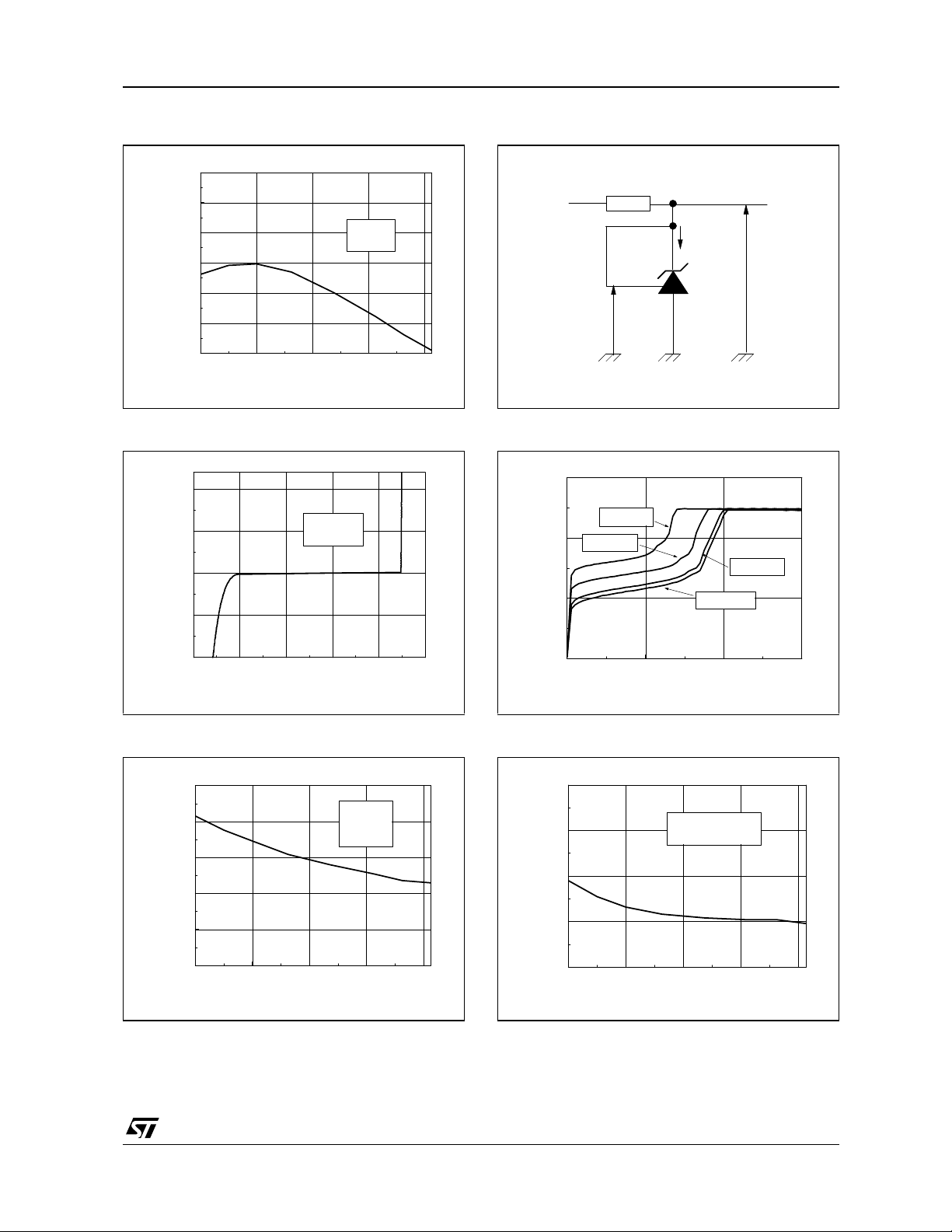
Reference voltage vs tempera ture
1.252
1.248
VK = V
1.244
1.240
1.236
Reference Voltage (V)
1.232
1.228
-40 0 40 80 120
Temperature (°C)
REF
IK = 100µA
Cathode voltage vs cathode curren t
10
VK = V
5
0
Cathode curren t (mA)
K
I
-5
T
AMB
REF
= +25°C
Test circuit for VK = V
REF
Input
Ik
K
V
VREF
Cathode voltage vs cathode curren t
1.5
T
=-40°C
AMB
1.0
T
=+25°C
AMB
T
=+85°C
AMB
Cathode voltage (V)
K
0.5
V
T
AMB
=+125°C
Output
-10
-1.0 -0.5 0.0 0.5 1.0 1.5
VK Cathode voltage (V)
Reference input current vs temperature
100
80
60
40
Reference current (nA)
REF
I
20
0
-40 0 40 80 120
Temperature (°C)
IK = 10 mA
= 10 KΩ
R
1
R2 = + ∞
0.0
0204060
IK Cathode current (µA)
Static impedance vs temperature
0.4
VK = V
0.3
0.2
Static impedance (Ohms)
KA
R
0.1
0.0
-40 0 40 80 120
Temperature (°C)
REF
IK = 100 µA to 12 mA
3/7

TS432
Off-State current vs temperature
150
V
= 0 V
100
Off-State current (nA)
50
OFF
I
0
-40 0 40 80 120
REF
= 10 V
V
K
Temperature (°C)
Ratio of change in reference input voltage to
change in V
voltage vs temperature
K
3
2
IK = 10 mA
= 10V to V
V
K
REF
Test circuit for Off-State current measurement
Input
Test circuit for V
KA
> V
REF
OFF
I
K =10V
V
Input
R1
K
I
REF
I
VK
1
0
Ratio of change in Reference input voltage (mV/V)
-40 0 40 80 120
Temperature (°C)
Phase and Gain vs frequency
60
Gain
40
Gain (dB)
Phase
20
0
2
10
3
10
10
Frequency (Hz)
T
4
10
= +25°C
AMB
5
R2
VREF
VK = VREF . (1+R1/R2) + IREF . R1
Test circuit for phase and gain measurement
180
Phase (Degree)
120
60
0
6
10
1 µ F
Input
23.5 kΩ
33 kΩ
33 kΩ
5V
22 µF
Output
4/7

TS432
Test circuit for pulse response at IK=100 µA
3V
0V
Pulse
Generator
f=10KHz
Intput
18K
Ω
IK = 100µA
Output
Pulse response at IK = 100 µA
3
Input
2
Output
Test circuit for pulse response at IK = 1 mA
3V
0V
Pulse
Generator
f=10KHz
Intput
1.8K
Ω
IK=1mA
Output
Pulse response at IK = 1mA
3
Input
2
IK = 1 mA
T
= + 25°C
AMB
1
Input and Ouput signals (Volt)
0
0 5 10 15
Time (µs)
Pulse response at IK = 100 µA
3
Input
2
1
Input and Outp ut signals (Volt)
0
0 5 10 15 20
Output
Time (µs)
IK = 100 µA
T
= + 25°C
AMB
IK = 100 µA
T
= + 25°C
AMB
1
Input and Outp ut signals (Volt)
0
0 5 10 15 20
Output
Time (µs)
Pulse response at IK = 1mA
3
Input
2
1
Input and Outp ut signals (Volt)
0
-5 0 5 10 15 20
Output
Time (µs)
IK = 1 mA
T
= + 25°C
AMB
5/7

TS432
Equivalent input noise vs frequency Block diagram
300
T
= + 25°C
AMB
200
Hz)
√
Noi se (nV/
100
Vref
Cathode
+
-
1.24V
0
2
3
4
10
10
10
Frequency (Hz)
5
10
6
10
7
10
Anode
6/7

PACKAGE MECHANICAL DATA
3 PINS - TINY PACKAGE (SOT23)
TS432
E
e
B
e1
S
L
H
A
D
A1
c
Millimeters Inches
Dim.
Min. Typ. Max. Min. Typ. Max.
A 0.890 1.120 0.035 0.044
A1 0.010 0.100 0.0004 0.004
A2 0.880 0.950 1.020 0.037 0.040
b 0.300 0.500 0.012 0.020
c 0.080 0.200 0.003 0.008
D 2.800 2.900 3.040 0.110 0.114 0.120
E 2.100 2.640 0.083 0.104
E1 1.200 1.300 1.400 0.047 0.051 0.055
e 0.950 0.037
e1 1.900 0.075
L 0.400 0.500 0.600 0.016 0.020 0.024
L1 0.540 0.021
k 0° 8°
Information furnished is bel ieved to be accurate and reliable. However, STMicroe lectronics assumes no responsibility for the
consequences of use of such information nor for any infringement of patents or other rights of third parties which may result from
its use. No li cense is granted by i mp lication or otherwise under any patent or patent rights of STMicroelectronics. Specifications
mentioned in this publication ar e subject to change without notice. This publication supersedes and replaces all information
previously supplied. S TMicroelectronics products are not authorized for use as critica l components in life suppo rt devices or
systems without express written approval of STMicroelectronics.
Australi a - Brazil - Chi na - Finlan d - F rance - Germ any - Hong Kong - India - Ital y - Japan - Ma l aysia - Malta - Morocco
© The ST logo is a registered trademark of STMicroelectronics
2002 STMi cr o electro n ics - All Righ ts Reserv ed
STMicr o el ectronics GROUP OF COMPA NI ES
Singapo re - Spain - Sweden - Swit zerland - United Kingdom
http://www.st.com
7/7
 Loading...