

1/32
■OPERATING FROM Vcc=2V to 5.5V
■STANDBY MODE A CTIV E HIGH (TS419) or
LOW (TS421)
■OUTPUT POWER into 16Ω: 367mW @ 5V
with 10% THD+N max or 295mW @5V and
110mW @3.3V with 1% THD+N max.
■LOW CURRENT CONSUMPTION: 2.5mA max
■High Signal-to-Noise ratio: 95dB(A) at 5V
■PSRR: 56dB typ. at 1kHz, 46dB at 217Hz
■SHORT CIRCUIT LIMITATION
■ON/OFF click reduction circuitry
■Available in SO8, MiniSO8 & DFN 3x3
DESCRIPTION
The TS419/TS421 is a monaural audio power amplifier driving in BTL mode a 16 or 32Ω earpiece or
receiver speaker. The main advantage of this configuration is to get rid of bulky ouput capacitors.
Capable of descending to lo w voltages , it delivers
up to 220mW per channel (into 16Ω loads) of continuous average power with 0.2% THD+N in the
audio bandwidth from a 5V power supply.
An externally controlled standby mode reduces
the supply current to 10nA (typ.). The TS419/
TS421 can be configu red by external gain-setting
resistors or used in a fixed gain version.
APPLICATIONS
■16/32 ohms earpiece or receiver speaker driver
■Mobile and cordless phones (analog / digital)
■PDAs & c o mpute r s
■Portable appliances
ORDER CODE
MiniSO & DFN only available in Tape & Reel with T suffix.
SO is available in Tube (D) and in Tape & Reel (DT)
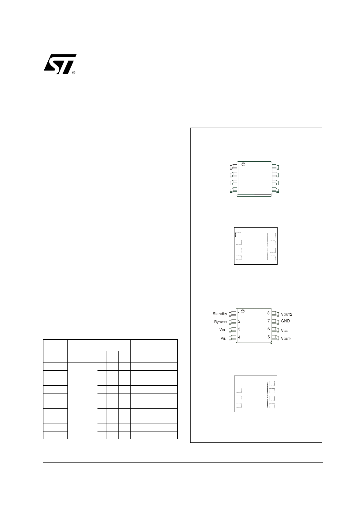
PIN CONNECTIONS (top view)
Part
Number
Temp.
Range:
I
Package
Gain Marking
DS Q
TS419
-40, +85°C
•
external TS419I
TS421
•
external TS421I
TS419
••
external K19A
TS419-2 tba tba x2/6dB K19B
TS419-4 tba tba x4/12dB K19C
TS419-8 tba tba x8/18dB K19D
TS421
••
external K21A
TS421-2 tba tba x2/6dB K21B
TS421-4 tba tba x4/12dB K21C
TS421-8 tba tba x8/18dB K21D
TS419IDT: SO8
TS419IST, TS419-xIST: MiniSO8
Standby
Bypass
V+
IN
V
IN-
V2
OUT
GND
V
CC
V
OUT1
1
2
3
4
8
7
6
5
TS421IDT: SO8
TS421IST, TS421-xIST: MiniSO8
TS419IQT, TS419-xIQT: DFN8
TS421IQT, TS421-xIQT: DFN8
1
2
3
4
5
8
7
6
STANDBY
BYPASS V
IN+
Vcc
V
OUT 1
GND
VIN-
VOUT 2
1
2
3
4
5
8
7
6
STANDBY
BYPASS V
IN+
Vcc
V
OUT 1
GND
VIN-
VOUT 2
1
2
3
4
5
8
7
6
STANDBY
BYPASS V
IN+
Vcc
V
OUT 1
GND
VIN-
VOUT 2
1
2
3
4
5
8
7
6
STANDBY
BYPASS V
IN+
Vcc
V
OUT 1
GND
VIN-
VOUT 2
TS419
TS421
360mW MONO AMPLIFIER WITH STANDBY MODE
June 2003
TS419-TS421
2/32
ABSOLUTE MAXIMUM RATINGS
OPERATING CONDITIONS
Symbol Parameter Value Unit
V
CC
Supply voltage
1)
6V
V
i
Input Voltage
-0.3V to V
CC
+0.3V
V
T
stg
Storage Temperature -65 to +150 °C
T
j
Maximum Junction Temperature 150 °C
R
thja
Thermal Resistance Junction to Ambient
SO8
MiniSO8
DFN8
175
215
70
°C/W
Pd
Power Dissipation
2)
SO8
MiniSO8
DFN8
0.71
0.58
1.79
W
ESD
Human Body Model (pin to pin): TS419
3)
, TS421
1.5 kV
ESD Machine Model - 220pF - 240pF (pin to pin) 100 V
Latch-up Latch-up Immunity (All pins) 200 mA
Lead Temperature (soldering, 10sec ) 250 °C
Output Short-Circuit to Vcc or GND
continous
4)
1. All voltage values are measured with respect to the ground pin.
2. Pd has been calculated with Tamb = 25°C, Tjunction = 150°C.
3. TS419 stands 1.5KV on all pi ns except sta ndby pin which st ands 1KV.
4. Attention must be pai d to continou s power dissipat i on (V
DD
x 300mA). Exposure of the IC to a short circuit for an extended time period is
dramatically reduci ng product lif e expectan cy .
Symbol Parameter Value Unit
V
CC
Supply Voltage 2 to 5.5 V
R
L
Load Resistor ≥ 16
Ω
T
oper
Operating Free Air Temperature Range -40 to + 85 °C
C
L
Load Capacitor
R
L
= 16 to 100
Ω
R
L
> 100
Ω
400
100
pF
V
ICM
Common Mode Input Voltage Range
GND to V
CC
-1V
V
V
STB
Standby Voltage Input
TS421 ACTIVE / TS419 in STANDBY
TS421 in STANDBY / TS419 ACTIVE
1.5 ≤ V
STB
≤ V
CC
GND ≤ V
STB
≤ 0.4
1)
V
R
THJA
Thermal Resistance Junction to Ambient
SO8
MiniSO8
DFN8
2)
150
190
41
°C/W
T
wu Wake-up time from standby to active mode (Cb = 1µF)
3)
≥
0.12 s
1. The minimum current consumption (I
STANDBY
) is guaranteed at VCC (TS419) or GND (TS421) for the whole temperature range.
2. Wh en m ounted on a 4-layer PCB
3. For more details on T
WU
, please refer to application note section on Wak e-up time pag e 28.
TS419-TS421
3/32
FIXED GAIN VERSION SPECIFIC ELECTRICAL CHARACTERISTI CS
V
CC
from +5V to +2V, GND = 0V, T
amb
= 25°C (unless otherwise specified)
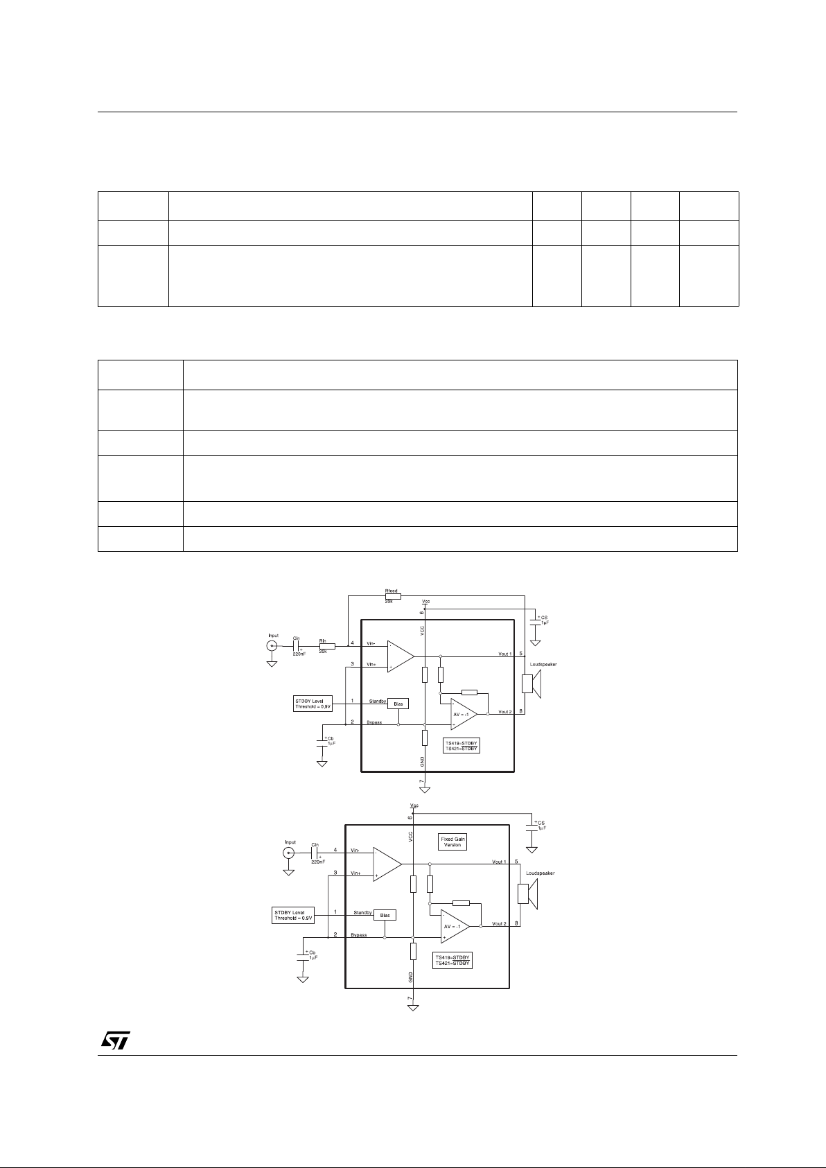
APPLICATION COMPONENTS INFORMATION
TYPICAL APPLICATION SCHEMATICS:
Symbol Parameter Min. Typ. Max. Unit
R
IN
Input Resistance 20 k
Ω
G
Gain value for Gain TS419/TS421-2
Gain value for Gain TS419/TS421-4
Gain value for Gain TS419/TS421-8
6dB
12dB
18dB
dB
Components Functional Description
R
IN
Inverting input resistor which sets the closed loop gain in conjunction with R
FEED
. This resistor also
forms a high pass filter with C
IN
(fcl = 1 / (2 x Pi x RIN x CIN)). Not needed in fixed gain versions.
C
IN
Input coupling capacitor which blocks the DC voltage at the amplifier’s input terminal
R
FEED
Feedback resistor which sets the closed loop gain in conjunction with RIN.
A
V
= Closed Loop Gain= 2xR
FEED/RIN
. Not needed in fixed gain versions.
C
S
Supply Bypass capacitor which provides power supply filtering.
C
B
Bypass capacitor which provides half supply filtering.
TS419-TS421
4/32
ELECTRICAL CHARACTERISTICS
V
CC
= +5V, GND = 0V , T
amb
= 25°C (unless otherwise specified)
Symbol Parameter Min. Typ. Max. Unit
I
CC
Supply Current
No input signal, no load 1.8 2.5 mA
I
STANDBY
Standby Current
No input signal, V
STANDBY
=GND for TS421
No input signal, V
STANDBY
=Vcc for TS419
10 1000 nA
Voo
Output Offset Voltage
No input signal, RL = 16 or 32
Ω,
Rfeed=20k
Ω
525mV
P
O
Output Power
THD+N = 0.1% Max, F = 1kHz, R
L
= 32
Ω
THD+N = 1% Max, F = 1kHz, R
L
= 32
Ω
THD+N = 10% Max, F = 1kHz, R
L
= 32
Ω
THD+N = 0.1% Max, F = 1kHz, R
L
= 16
Ω
THD+N = 1% Max, F = 1kHz, R
L
= 16
Ω
THD+N = 10% Max, F = 1kHz, R
L
= 16
Ω
166
240
190
207
258
270
295
367
mW
THD + N
Total Harmonic Distortion + Noise (A
v
=2)
R
L
= 32
Ω,
P
out
= 150mW, 20Hz ≤ F ≤ 20kHz
R
L
= 16
Ω,
P
out
= 220mW, 20Hz ≤ F ≤ 20kHz
0.15
0.2
%
PSRR
Power Supply Rejection Ratio (A
v
=2)
1)
F = 1kHz, Vripple = 200mVpp, input grounded, Cb=1µF
1. Guaranteed by design and evaluation.
50 56 dB
SNR
Signal-to-Noise Ratio (Filter Type A, A
v
=2)
1)
(RL = 32
Ω,
THD +N < 0.5%, 20Hz ≤ F ≤ 20kHz)
85 98 dB
Φ
M
Phase Margin at Unity Gain
R
L
= 16Ω, CL = 400pF
58 Degrees
GM
Gain Margin
R
L
= 16Ω, CL = 400pF
18 dB
GBP
Gain Bandwidth Product
R
L
= 16
Ω
1.1 MHz
SR
Slew Rate
R
L
= 16
Ω
0.4 V/µS
TS419-TS421
5/32
ELECTRICAL CHARACTERISTICS
V
CC
= +3.3V, GND = 0V, T
amb
= 25°C (unless otherwise specified)
1)
1. All electrical values are guaranted with correlation measurements at 2V and 5V
Symbol Parameter Min. Typ. Max. Unit
I
CC
Supply Current
No input signal, no load 1.8 2.5 mA
I
STANDBY
Standby Current
No input signal, V
STANDBY
=GND for TS421
No input signal, V
STANDBY
=Vcc for TS419
10 1000 nA
Voo
Output Offset Voltage
No input signal, RL = 16 or 32Ω, Rfeed=20k
Ω
525mV
P
O
Output Power
THD+N = 0.1% Max, F = 1kHz, R
L
= 32
Ω
THD+N = 1% Max, F = 1kHz, R
L
= 32
Ω
THD+N = 10% Max, F = 1kHz, R
L
= 32
Ω
THD+N = 0.1% Max, F = 1kHz, R
L
= 16
Ω
THD+N = 1% Max, F = 1kHz, R
L
= 16
Ω
THD+N = 10% Max, F = 1kHz, R
L
= 16
Ω
65
91
75
81
102
104
113
143
mW
THD + N
Total Harmonic Distortion + Noise (A
v
=2)
R
L
= 32
Ω,
P
out
= 50mW, 20Hz ≤ F ≤ 20kHz
R
L
= 16
Ω,
P
out
= 70mW, 20Hz ≤ F ≤ 20kHz
0.15
0.2
%
PSRR
Power Supply Rejection Ratio
inputs grounded, F = 1kHz, Vripple = 200mVpp, Cb=1µF
50 56 dB
SNR
Signal-to-Noise Ratio (Weighted A, A
v
=2)
(R
L
= 32
Ω,
THD +N < 0.5%, 20Hz ≤ F ≤ 20kHz)
82 94 dB
Φ
M
Phase Margin at Unity Gain
R
L
= 16Ω, CL = 400pF
58 Degrees
GM
Gain Margin
R
L
= 16Ω, CL = 400pF
18 dB
GBP
Gain Bandwidth Product
R
L
= 16
Ω
1.1 MHz
SR
Slew Rate
R
L
= 16
Ω
0.4 V/µS
TS419-TS421
6/32
ELECTRICAL CHARACTERISTICS
V
CC
= +2.5V, GND = 0V, T
amb
= 25°C (unless otherwise specified)
1)
1. All electrical values are guaranted with correlation measurements at 2V and 5V
Symbol Parameter Min. Typ. Max. Unit
I
CC
Supply Current
No input signal, no load 1.7 2.5 mA
I
STANDBY
Standby Current
No input signal, V
STANDBY
=GND for TS421
No input signal, V
STANDBY
=Vcc for TS419
10 1000 nA
Voo
Output Offset Voltage
No input signal, RL = 16 or 32
Ω,
Rfeed=20k
Ω
525mV
P
O
Output Power
THD+N = 0.1% Max, F = 1kHz, R
L
= 32
Ω
THD+N = 1% Max, F = 1kHz, R
L
= 32
Ω
THD+N = 10% Max, F = 1kHz, R
L
= 32
Ω
THD+N = 0.1% Max, F = 1kHz, R
L
= 16
Ω
THD+N = 1% Max, F = 1kHz, R
L
= 16
Ω
THD+N = 10% Max, F = 1kHz, R
L
= 16
Ω
32
44
37
41
52
50
55
70
mW
THD + N
Total Harmonic Distortion + Noise (A
v
=2)
R
L
= 32
Ω,
P
out
= 30mW, 20Hz ≤ F ≤ 20kHz
R
L
= 16
Ω,
P
out
= 40mW, 20Hz ≤ F ≤ 20kHz
0.15
0.2
%
PSRR
Power Supply Rejection Ratio (A
v
=2)
inputs grounded, F = 1kHz, Vripple = 200mVpp, Cb=1µF
50 56 dB
SNR
Signal-to-Noise Ratio (Weighted A, A
v
=2)
(R
L
= 32
Ω,
THD +N < 0.5%, 20Hz ≤ F ≤ 20kHz)
80 91 dB
Φ
M
Phase Margin at Unity Gain
R
L
= 16Ω, CL = 400pF
58 Degrees
GM
Gain Margin
R
L
= 16Ω, CL = 400pF
18 dB
GBP
Gain Bandwidth Product
R
L
= 16
Ω
1.1 MHz
SR
Slew Rate
R
L
= 16
Ω
0.4 V/µS

TS419-TS421
7/32
ELECTRICAL CHARACTERISTICS
V
CC
= +2V, GND = 0V, T
amb
= 25°C (unless otherwise specified)
Symbol Parameter Min. Typ. Max. Unit
I
CC
Supply Current
No input signal, no load 1.7 2.5 mA
I
STANDBY
Standby Current
No input signal, V
STANDBY
=GND for TS421
No input signal, V
STANDBY
=Vcc for TS419
10 1000 nA
Voo
Output Offset Voltage
No input signal, RL = 16 or 32
Ω,
Rfeed=20k
Ω
525mV
P
O
Output Power
THD+N = 0.1% Max, F = 1kHz, R
L
= 32
Ω
THD+N = 1% Max, F = 1kHz, R
L
= 32
Ω
THD+N = 10% Max, F = 1kHz, R
L
= 32
Ω
THD+N = 0.1% Max, F = 1kHz, R
L
= 16
Ω
THD+N = 1% Max, F = 1kHz, R
L
= 16
Ω
THD+N = 10% Max, F = 1kHz, R
L
= 16
Ω
19
24
20
23
30
26
30
40
mW
THD + N
Total Harmonic Distortion + Noise (A
v
=2)
R
L
= 32
Ω,
P
out
= 13mW, 20Hz ≤ F ≤ 20kHz
R
L
= 16
Ω,
P
out
= 20mW, 20Hz ≤ F ≤ 20kHz
0.1
0.15
%
PSRR
Power Supply Rejection Ratio (A
v
=2)
1)
inputs grounded, F = 1kHz, Vripple = 200mVpp, Cb=1µF
1. Guaranteed by design and evaluation.
49 54 dB
SNR
Signal-to-Noise Ratio (Weighted A, A
v
=2)
1)
(RL = 32
Ω,
THD +N < 0.5%, 20Hz ≤ F ≤ 20kHz)
80 89 dB
Φ
M
Phase Margin at Unity Gain
R
L
= 16Ω, CL = 400pF
58 Degrees
GM
Gain Margin
R
L
= 16Ω, CL = 400pF
20 dB
GBP
Gain Bandwidth Product
R
L
= 16
Ω
1.1 MHz
SR
Slew Rate
R
L
= 16
Ω
0.4 V/µS

TS419-TS421
8/32
Index of Graphs
Note : All measurements made with Rin=20kΩ, Cb=1µF, and Cin=10µF unless otherwise specified.
Description Figure Page
Common Curves
Open Loop Gain and Phase vs Frequency 1 to 12 9 to 10
Current Consumption vs Power Supply Voltage 13 11
Current Consumption vs Standby Voltage 14 to 19 11 to 12
Output Power vs Power Supply Voltage 20 to 23 12
Output Power vs Load Resistor 24 to 27 12 to 13
Power Dissipation vs Output Power 28 to 31 13 to 14
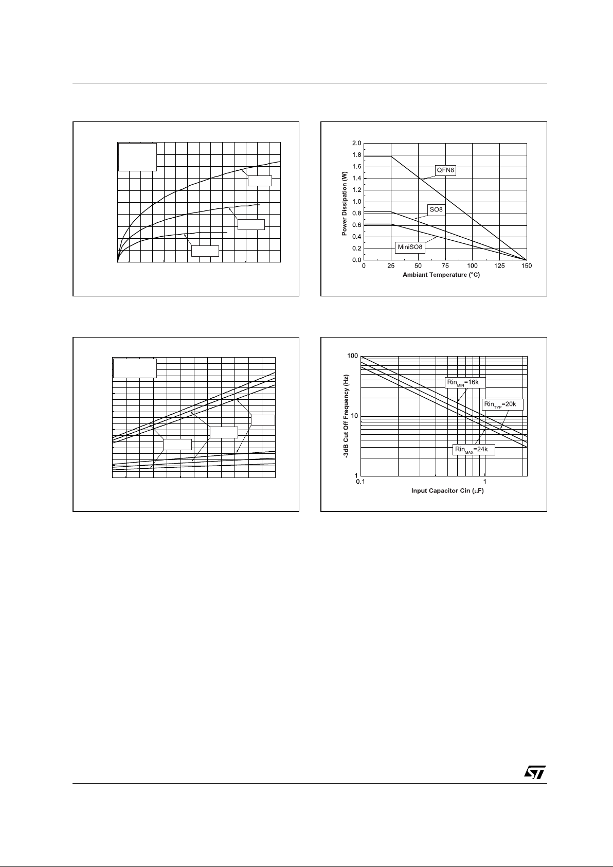
Power Derating vs Ambiant Temperature 32 14
Output Voltage Swing vs Supply Voltage 33 14
Low Frequency Cut Off vs Input Capacitor 34 14
Curves With 6dB Gain Setting (Av=2)
THD + N vs Output Power 35 to 43 15 to 16
THD + N vs Frequency 44 to 46 16
Signal to Noise Ratio vs Power Supply Voltage 47 to 48 17
Noise Floor 49 to 50 17
PSRR vs Frequency 51 to 55 17 to 18
Curves With 12dB Gain Setting (Av=4)
THD + N vs Output Power 56 to 64 19 to 20
THD + N vs Frequency 65 to 67 20
Signal to Noise Ratio vs Power Supply Voltage 68 to 69 21
Noise Floor 70 to 71 21
PSRR vs Frequency 72 to 76 21 to 22
Curves With 18dB Gain Setting (Av=8)
THD + N vs Output Power 77 to 85 23 to 24
THD + N vs Frequency 86 to 88 24
Signal to Noise Ratio vs Power Supply Voltage 89 to 90 25
Noise Floor 91 to 92 25
PSRR vs Frequency 93 to 97 25 to 26
TS419-TS421
9/32
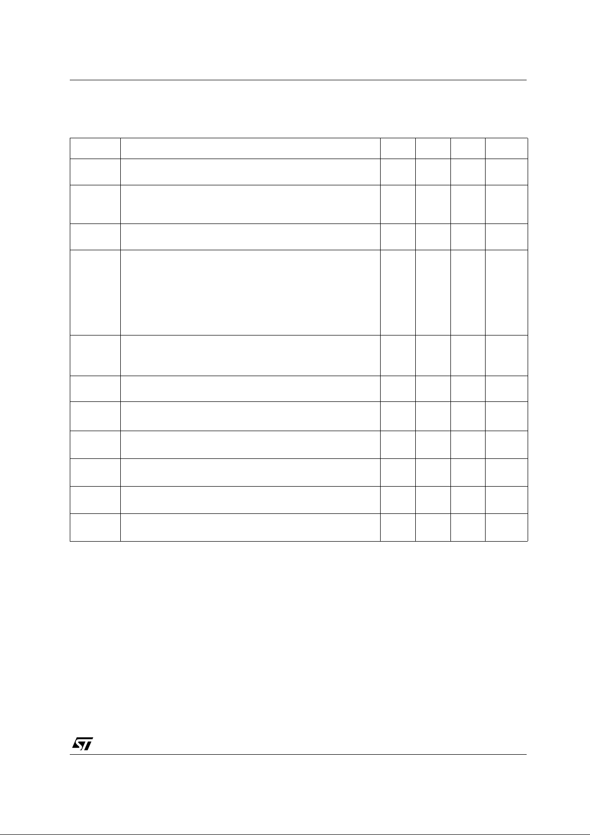
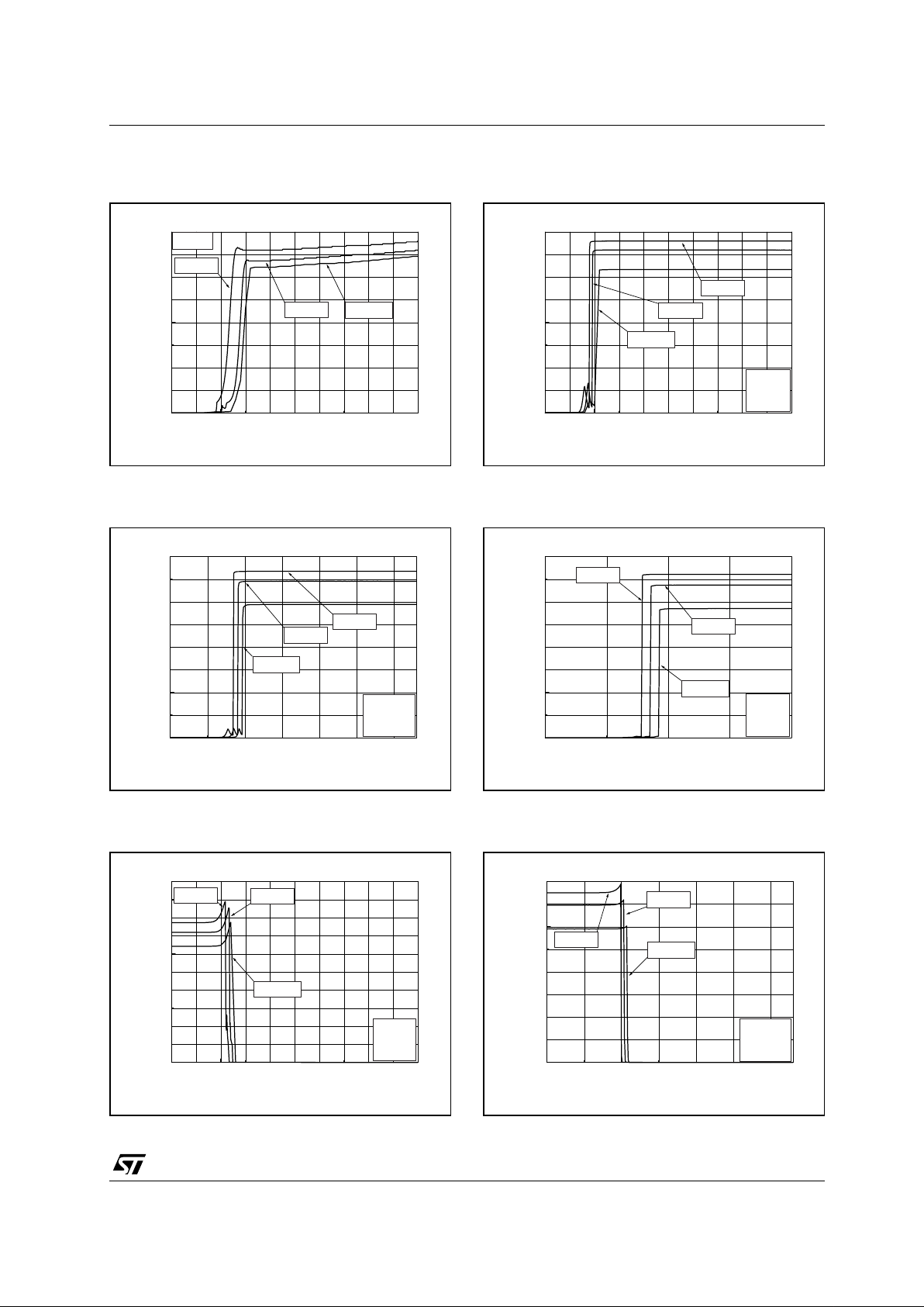
Fig. 1: Open Loop Gain and Phase vs
Frequency
Fig. 3: Open Loop Gain and Phase vs
Frequency
Fig. 5: Open Loop Gain and Phase vs
Frequency
Fig. 2: Open Loop Gain and Phase vs
Frequency
Fig. 4: Open Loop Gain and Phase vs
Frequency
Fig. 6: Open Loop Gain and Phase vs
Frequency
0.1 1 10 100 1000 10000
-40
-20
0
20
40
60
80
-20
0
20
40
60
80
100
120
140
160
180
Gain (dB)
Frequency (kHz)
Vcc = 5V
RL = 8
Ω
Tamb = 25°C
Gain
Phase
Phase (Deg)
0.1 1 10 100 1000 10000
-40
-20
0
20
40
60
80
-20
0
20
40
60
80
100
120
140
160
180
Gain (dB)
Frequency (kHz)
Vcc = 5V
ZL = 8Ω+400pF
Tamb = 25°C
Gain
Phase
Phase (Deg)
0.1 1 10 100 1000 10000
-40
-20
0
20
40
60
80
-20
0
20
40
60
80
100
120
140
160
180
Gain (dB)
Frequency (kHz)
Vcc = 5V
RL = 16
Ω
Tamb = 25°C
Gain
Phase
Phase (Deg)
0.1 1 10 100 1000 10000
-40
-20
0
20
40
60
80
-20
0
20
40
60
80
100
120
140
160
180
Gain (dB)
Frequency (kHz)
Vcc = 2V
RL = 8
Ω
Tamb = 25°C
Gain
Phase
Phase (Deg)
0.1 1 10 100 1000 10000
-40
-20
0
20
40
60
80
-20
0
20
40
60
80
100
120
140
160
180
Gain (dB)
Frequency (kHz)
Vcc = 2V
ZL = 8Ω+400pF
Tamb = 25°C
Gain
Phase
Phase (Deg)
0.1 1 10 100 1000 10000
-40
-20
0
20
40
60
80
-20
0
20
40
60
80
100
120
140
160
180
Gain (dB)
Frequency (kHz)
Vcc = 2V
RL = 16
Ω
Tamb = 25°C
Gain
Phase
Phase (Deg)
TS419-TS421
10/32
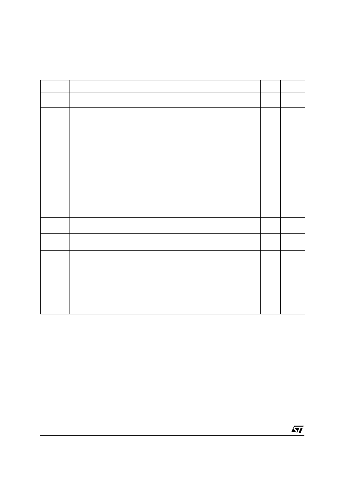
Fig. 7: Open Loop Gain and Phase vs
Frequency
Fig. 9: Open Loop Gain and Phase vs
Frequency
Fig. 11: Open Loop Gain and Phase vs
Frequency
Fig. 8: Open Loop Gain and Phase vs
Frequency
Fig. 10: Open Loop Gain and Phase vs
Frequency
Fig. 12: Open Loop Gain and Phase vs
Frequency
0.1 1 10 100 1000 10000
-40
-20
0
20
40
60
80
-20
0
20
40
60
80
100
120
140
160
180
Gain (dB)
Frequency (kHz)
Vcc = 5V
ZL = 16Ω+400pF
Tamb = 25°C
Gain
Phase
Phase (Deg)
0.1 1 10 100 1000 10000
-40
-20
0
20
40
60
80
-20
0
20
40
60
80
100
120
140
160
180
Gain (dB)
Frequency (kHz)
Vcc = 5V
RL = 32
Ω
Tamb = 25°C
Gain
Phase
Phase (Deg)
0.1 1 10 100 1000 10000
-40
-20
0
20
40
60
80
-20
0
20
40
60
80
100
120
140
160
180
Gain (dB)
Frequency (kHz)
Vcc = 5V
ZL = 32Ω+400pF
Tamb = 25°C
Gain
Phase
Phase (Deg)
0.1 1 10 100 1000 10000
-40
-20
0
20
40
60
80
-20
0
20
40
60
80
100
120
140
160
180
Gain (dB)
Frequency (kHz)
Vcc = 2V
ZL = 16Ω+400pF
Tamb = 25°C
Gain
Phase
Phase (Deg)
0.1 1 10 100 1000 10000
-40
-20
0
20
40
60
80
-20
0
20
40
60
80
100
120
140
160
180
Gain (dB)
Frequency (kHz)
Vcc = 2V
RL = 32
Ω
Tamb = 25°C
Gain
Phase
Phase (Deg)
0.1 1 10 100 1000 10000
-40
-20
0
20
40
60
80
-20
0
20
40
60
80
100
120
140
160
180
Gain (dB)
Frequency (kHz)
Vcc = 2V
ZL = 32Ω+400pF
Tamb = 25°C
Gain
Phase
Phase (Deg)
TS419-TS421
11/32
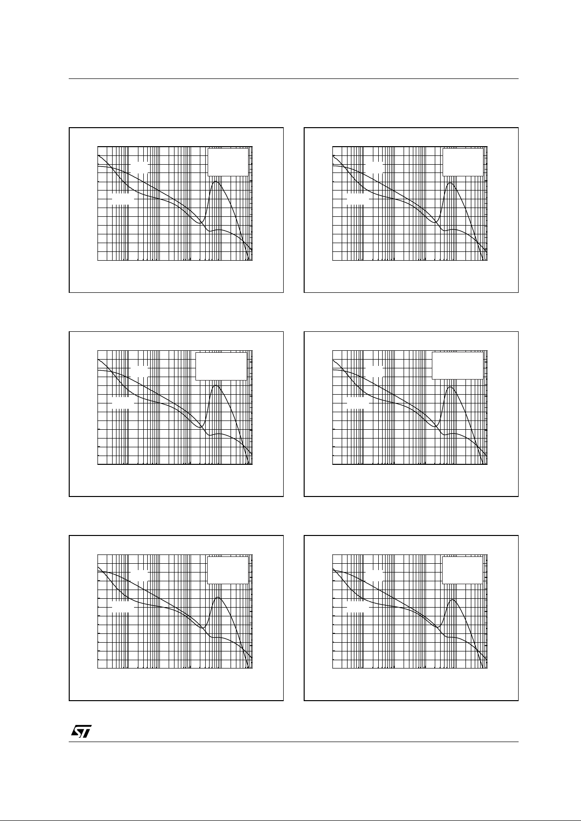
Fig. 13: Current Consumption vs Power Supply
Voltage
Fig. 15: Current Consumption vs Standby
Voltage
Fig. 17: Current Consumption vs Standby
Voltage
Fig. 14: Current Consumption vs Standby
Voltage
Fig. 16: Current Consumption vs Standby
Voltage
Fig. 18: Current Consumption vs Standby
Voltage
012345
0.0
0.5
1.0
1.5
2.0
Ta=85°C
Ta=25°C
No load
Ta=-40°C
Current Consumption (mA)
Power Supply Voltage (V)
0123
0.0
0.5
1.0
1.5
2.0
Ta=85°C
Ta=25°C
TS419
Vcc = 3.3V
No load
Ta=-40°C
Current Consumption (mA)
Standby Voltage (V)
012345
0.0
0.5
1.0
1.5
2.0
2.5
Ta=85°C
Ta=25°C
TS421
Vcc = 5V
No load
Ta=-40°C
Current Consumption (mA)
Standby Voltage (V)
012345
0.0
0.5
1.0
1.5
2.0
Ta=85°C
Ta=25°C
TS419
Vcc = 5V
No load
Ta=-40°C
Current Consumption (mA)
Standby Voltage (V)
012
0.0
0.5
1.0
1.5
2.0
Ta=85°C
Ta=25°C
TS419
Vcc = 2V
No load
Ta=-40°C
Current Consumption (mA)
Standby Voltage (V)
0123
0.0
0.5
1.0
1.5
2.0
Ta=85°C
Ta=25°C
TS421
Vcc = 3.3V
No load
Ta=-40°C
Current Consumption (mA)
Standby Voltage (V)

TS419-TS421
12/32
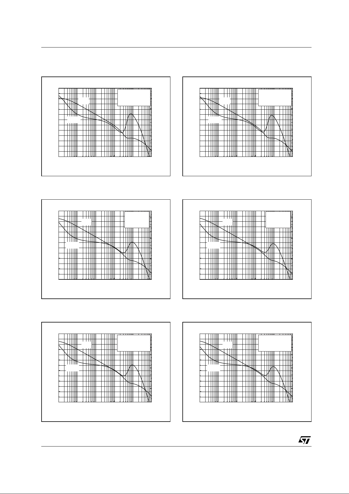
Fig. 19: Current Consumption vs Standby
Voltage
Fig. 21: Output P owe r vs Po wer S up pl y
Voltage
Fig. 23: Output P owe r vs Po wer S up pl y
Voltage
Fig. 20: Output P owe r vs Power S up pl y
Voltage
Fig. 22: Output P owe r vs Power S up pl y
Voltage
Fig. 24: Output Power vs Load Resistor
012
0.0
0.5
1.0
1.5
2.0
Ta=85°C
Ta=25°C
TS421
Vcc = 2V
No load
Ta=-40°C
Current Consumption (mA)
Standby Voltage (V)
2.0 2.5 3.0 3.5 4.0 4.5 5.0 5.5
0
50
100
150
200
250
300
350
400
450
500
THD+N=10%
THD+N=0.1%
RL = 16
Ω
F = 1kHz
BW < 125kHz
Tamb = 25°C
THD+N=1%
Output power (mW)
Vcc (V)
2.0 2.5 3.0 3.5 4.0 4.5 5.0 5.5
0
50
100
150
200
THD+N=10%
THD+N=0.1%
RL = 64
Ω
F = 1kHz
BW < 125kHz
Tamb = 25°C
THD+N=1%
Output power (mW)
Vcc (V)
2.0 2.5 3.0 3.5 4.0 4.5 5.0 5.5
0
50
100
150
200
250
300
350
400
450
500
550
THD+N=10%
THD+N=0.1%
RL = 8
Ω
F = 1kHz
BW < 125kHz
Tamb = 25°C
THD+N=1%
Output power (mW)
Vcc (V)
2.0 2.5 3.0 3.5 4.0 4.5 5.0 5.5
0
50
100
150
200
250
300
THD+N=10%
THD+N=0.1%
RL = 32
Ω
F = 1kHz
BW < 125kHz
Tamb = 25°C
THD+N=1%
Output power (mW)
Vcc (V)
8 16243240485664
0
50
100
150
200
250
300
350
400
450
500
THD+N=10%
THD+N=0.1%
Vcc = 5V
F = 1kHz
BW < 125kHz
Tamb = 25°C
THD+N=1%
Output power (mW)
Load Resistance ( )

TS419-TS421
13/32
Fig. 25: Output Power vs Load Resistor
Fig. 27: Output Power vs Load Resistor
Fig. 29: Power Dissipation vs Output Power
Fig. 26: Output Power vs Load Resistor
Fig. 28: Power Dissipation vs Output Power
Fig. 30: Power Dissipation vs Output Power
8 16243240485664
0
50
100
150
200
THD+N=10%
THD+N=0.1%
Vcc = 3.3V
F = 1kHz
BW < 125kHz
Tamb = 25°C
THD+N=1%
Output power (mW)
Load Resistance ( )
8 16243240485664
0
5
10
15
20
25
30
35
40
45
50
THD+N=10%
THD+N=0.1%
Vcc = 2V
F = 1kHz
BW < 125kHz
Tamb = 25°C
THD+N=1%
Output power (mW)
Load Resistance ( )
0 30 60 90 120 150
0
50
100
150
200
250
300
RL=32
Ω
RL=8
Ω
Vcc=3.3V
F=1kHz
THD+N<1%
RL=16
Ω
Power Dissipation (mW)
Output Power (mW)
8 16243240485664
0
10
20
30
40
50
60
70
80
90
100
THD+N=10%
THD+N=0.1%
Vcc = 2.5V
F = 1kHz
BW < 125kHz
Tamb = 25°C
THD+N=1%
Output power (mW)
Load Resistance ( )
0 50 100 150 200 250 300 350
0
100
200
300
400
500
600
RL=16Ω
RL=8Ω
Vcc=5V
F=1kHz
THD+N<1%
RL=32Ω
Power Dissipation (mW)
Output Power (mW)
0 102030405060
0
20
40
60
80
100
120
140
RL=32
Ω
RL=8
Ω
Vcc=2.5V
F=1kHz
THD+N<1%
RL=16
Ω
Power Dissipation (mW)
Output Power (mW)
TS419-TS421
14/32
Fig. 31: Power Dissipation vs Output Power
Fig. 33: Output Voltage Swing For One Amp. vs
Power Supply Volt a ge
Fig. 32: Power Derating Curves
Fig. 34 : Low Freque ncy Cut Off vs Inp ut
Capacitor for fixed gain versions
0 5 10 15 20 25 30 35
0
20
40
60
80
100
RL=8
Ω
RL=16
Ω
RL=32
Ω
Vcc=2V
F=1kHz
THD+N<1%
Power Dissipation (mW)
Output Power (mW)
2.0 2.5 3.0 3.5 4.0 4.5 5.0
0.0
0.5
1.0
1.5
2.0
2.5
3.0
3.5
4.0
4.5
5.0
RL=8
Ω
RL=32
Ω
RL=16
Ω
Tamb=25°C
Amps. in BTL
VOH & VOL for Vs1 and Vs2 (V)
Power Supply Voltage (V)
Ω
Ω
Ω

TS419-TS421
15/32
Fig. 35: THD + N vs Output Power
Fig. 37: THD + N vs Output Power
Fig. 39: THD + N vs Output Power
Fig. 36: THD + N vs Output Power
Fig. 38: THD + N vs Output Power
Fig. 40: THD + N vs Output Power
1 10 100
1E-3
0.01
0.1
1
10
Vcc=5V
Vcc=3.3V
Vcc=2.5V
Vcc=2V
RL = 8
Ω
F = 20Hz
Av = 2
Cb = 1µF
BW < 22kHz
Tamb = 25°C
THD + N (%)
Output Power (mW)
1 10 100
1E-3
0.01
0.1
1
10
Vcc=5V
Vcc=3.3V
Vcc=2.5V
Vcc=2V
RL = 32
Ω
F = 20Hz
Av = 2
Cb = 1µF
BW < 22kHz
Tamb = 25°C
THD + N (%)
Output Power (mW)
1 10 100
0.01
0.1
1
10
Vcc=5V
Vcc=3.3V
Vcc=2.5V
Vcc=2V
RL = 16
Ω
F = 1kHz
Av = 2
Cb = 1µF
BW < 125kHz
Tamb = 25°C
THD + N (%)
Output Power (mW)
1 10 100
1E-3
0.01
0.1
1
10
Vcc=5V
Vcc=3.3V
Vcc=2.5V
Vcc=2V
RL = 16
Ω
F = 20Hz
Av = 2
Cb = 1µF
BW < 22kHz
Tamb = 25°C
THD + N (%)
Output Power (mW)
1 10 100
0.01
0.1
1
10
Vcc=5VVcc=3.3V
Vcc=2.5V
Vcc=2V
RL = 8
Ω
F = 1kHz
Av = 2
Cb = 1µF
BW < 125kHz
Tamb = 25°C
THD + N (%)
Output Power (mW)
1 10 100
1E-3
0.01
0.1
1
10
Vcc=5V
Vcc=3.3V
Vcc=2.5V
Vcc=2V
RL = 32
Ω
F = 1kHz
Av = 2
Cb = 1µF
BW < 125kHz
Tamb = 25°C
THD + N (%)
Output Power (mW)

TS419-TS421
16/32
Fig. 41: THD + N vs Output Power
Fig. 43: THD + N vs Output Power
Fig. 45: THD + N vs Frequency
Fig. 42: THD + N vs Output Power
Fig. 44: THD + N vs Frequency
Fig. 46: THD + N vs Frequency
1 10 100
0.1
1
10
Vcc=5V
Vcc=3.3V
Vcc=2.5V
Vcc=2V
RL = 8
Ω
F = 20kHz
Av = 2
Cb = 1µF
BW < 125kHz
Tamb = 25°C
THD + N (%)
Output Power (mW)
1 10 100
0.1
1
10
Vcc=5V
Vcc=3.3V
Vcc=2.5V
Vcc=2V
RL = 32
Ω
F = 20kHz
Av = 2
Cb = 1µF
BW < 125kHz
Tamb = 25°C
THD + N (%)
Output Power (mW)
100 1000 10000
0.01
0.1
Vcc=2V, Po=20mW
Vcc=5V, Po=220mW
RL=16
Ω
Av=2
Cb = 1µF
Bw < 125kHz
Tamb = 25°C
20k20
THD + N (%)
Frequency (Hz)
1 10 100
0.1
1
10
Vcc=5V
Vcc=3.3V
Vcc=2.5V
Vcc=2V
RL = 16
Ω
F = 20kHz
Av = 2
Cb = 1µF
BW < 125kHz
Tamb = 25°C
THD + N (%)
Output Power (mW)
100 1000 10000
0.01
0.1
Vcc=2V, Po=28mW
Vcc=5V, Po=300mW
RL=8
Ω
Av=2
Cb = 1µF
Bw < 125kHz
Tamb = 25°C
20k20
THD + N (%)
Frequency (Hz)
100 1000 10000
0.01
0.1
Vcc=2V, Po=13mW
Vcc=5V, Po=150mW
RL=32Ω
Av=2
Cb = 1µF
Bw < 125kHz
Tamb=25°C
20k20
THD + N (%)
Frequency (Hz)

TS419-TS421
17/32
Fig. 47: Signal to Noise Ratio vs Power Supply
Voltage with Unweighted Filter (20Hz to 20kHz)
Fig. 49: Noise Floor
Fig. 51: PSRR vs Input Capacitor
Fig. 48: Signal to Noise Ratio vs Power Supply
Voltage with Weighted Filter Type A
Fig. 50: Noise Floor
Fig. 52: PSRR vs Power Supply Voltage
2.0 2.5 3.0 3.5 4.0 4.5 5.0
70
75
80
85
90
95
100
Av = 2
Cb = 1µF
THD+N < 0.5%
Tamb = 25°C
RL=32
Ω
RL=16
Ω
RL=8
Ω
Signal to Noise Ratio (dB)
Power Supply Voltage (V)
100 1000 10000
0
10
20
30
Standby=OFF
Standby=ON
RL>=16
Ω
Vcc=5V
Av=2
Cb = 1µF
Input Grounded
Bw < 125kHz
Tamb=25°C
20k20
Noise Floor ( VRms)
Frequency (Hz)
100 1000 10000 100000
-70
-60
-50
-40
-30
-20
-10
0
Cin = 100nF
Cin = 1µF, 220nF
Vripple = 200mVpp
Av = 2, Vcc = 5V
Input = grounded
Cb = 1µF, Rin = 20kΩ
RL >= 16Ω
Tamb = 25°C
PSRR (dB)
Frequency (Hz)
2.0 2.5 3.0 3.5 4.0 4.5 5.0
80
85
90
95
100
105
Av = 2
Cb = 1µF
THD+N < 0.5%
Tamb = 25°C
RL=32
Ω
RL=16
Ω
RL=8
Ω
Signal to Noise Ratio (dB)
Power Supply Voltage (V)
100 1000 10000
0
10
20
30
Standby=OFF
Standby=ON
RL>=16
Ω
Vcc=2V
Av=2
Cb = 1µF
Input Grounded
Bw < 125kHz
Tamb=25°C
20k20
Noise Floor ( VRms)
Frequency (Hz)
100 1000 10000 100000
-80
-70
-60
-50
-40
-30
-20
-10
0
Vcc = 2V
Vcc = 5V, 3.3V & 2.5V
Vripple = 100mVrms
Rfeed = 20kΩ
Input = floating
Cb = 1µF
RL >= 16Ω
Tamb = 25°C
PSRR (dB)
Frequency (Hz)

TS419-TS421
18/32
Fig. 53: PSRR vs Bypass Capacitor
Fig. 55: PSRR vs Bypass Capacitor
Fig. 54: PSRR vs Bypass Capacitor
100 1000 10000 100000
-70
-60
-50
-40
-30
-20
-10
0
Vcc = 2V
Vcc = 5V, 3.3V & 2.5V
Vripple = 200mVpp
Av = 2
Input = Grounded
Cb = Cin = 1µF
RL >= 16Ω
Tamb = 25°C
PSRR (dB)
Frequency (Hz)
100 1000 10000 100000
-70
-60
-50
-40
-30
-20
-10
0
Vcc = 2V
Vcc = 5V, 3.3V & 2.5V
Vripple = 200mVpp
Av = 2
Input = Grounded
Cb = 10µF
Cin = 1µF
RL >= 16Ω
Tamb = 25°C
PSRR (dB)
Frequency (Hz)
100 1000 10000 100000
-70
-60
-50
-40
-30
-20
-10
0
Vcc = 2V
Vcc = 5V, 3.3V & 2.5V
Vripple = 200mVpp
Av = 2
Input = Grounded
Cb = 4.7µF
Cin = 1µF
RL >= 16Ω
Tamb = 25°C
PSRR (dB)
Frequency (Hz)

TS419-TS421
19/32
Fig. 56: THD + N vs Output Power
Fig. 58: THD + N vs Output Power
Fig. 60: THD + N vs Output Power
Fig. 57: THD + N vs Output Power
Fig. 59: THD + N vs Output Power
Fig. 61: THD + N vs Output Power
1 10 100
0.01
0.1
1
10
Vcc=5V
Vcc=3.3V
Vcc=2.5V
Vcc=2V
RL = 8
Ω
F = 20Hz
Av = 4
Cb = 1µF
BW < 22kHz
Tamb = 25°C
THD + N (%)
Output Power (mW)
1 10 100
1E-3
0.01
0.1
1
10
Vcc=5V
Vcc=3.3V
Vcc=2.5V
Vcc=2V
RL = 32
Ω
F = 20Hz
Av = 4
Cb = 1µF
BW < 22kHz
Tamb = 25°C
THD + N (%)
Output Power (mW)
1 10 100
0.01
0.1
1
10
Vcc=5V
Vcc=3.3V
Vcc=2.5V
Vcc=2V
RL = 16
Ω
F = 1kHz
Av = 4
Cb = 1µF
BW < 125kHz
Tamb = 25°C
THD + N (%)
Output Power (mW)
1 10 100
1E-3
0.01
0.1
1
10
Vcc=5V
Vcc=3.3V
Vcc=2.5V
Vcc=2V
RL = 16
Ω
F = 20Hz
Av = 4
Cb = 1µF
BW < 22kHz
Tamb = 25°C
THD + N (%)
Output Power (mW)
1 10 100
0.01
0.1
1
10
Vcc=5VVcc=3.3V
Vcc=2.5V
Vcc=2V
RL = 8
Ω
F = 1kHz
Av = 4
Cb = 1µF
BW < 125kHz
Tamb = 25°C
THD + N (%)
Output Power (mW)
1 10 100
1E-3
0.01
0.1
1
10
Vcc=5V
Vcc=3.3V
Vcc=2.5V
Vcc=2V
RL = 32
Ω
F = 1kHz
Av = 4
Cb = 1µF
BW < 125kHz
Tamb = 25°C
THD + N (%)
Output Power (mW)

TS419-TS421
20/32
Fig. 62: THD + N vs Output Power
Fig. 64: THD + N vs Output Power
Fig. 66: THD + N vs Frequency
Fig. 63: THD + N vs Output Power
Fig. 65: THD + N vs Frequency
Fig. 67: THD + N vs Frequency
1 10 100
1
10
Vcc=5V
Vcc=3.3V
Vcc=2.5V
Vcc=2V
RL = 8
Ω
F = 20kHz
Av = 4
Cb = 1µF
BW < 125kHz
Tamb = 25°C
THD + N (%)
Output Power (mW)
1 10 100
0.1
1
10
Vcc=5V
Vcc=3.3V
Vcc=2.5V
Vcc=2V
RL = 32
Ω
F = 20kHz
Av = 4
Cb = 1µF
BW < 125kHz
Tamb = 25°C
THD + N (%)
Output Power (mW)
100 1000 10000
0.01
0.1
Vcc=2V, Po=20mW
Vcc=5V, Po=220mW
RL=16
Ω
Av=4
Cb = 1µF
Bw < 125kHz
Tamb = 25°C
20k20
THD + N (%)
Frequency (Hz)
1 10 100
0.1
1
10
Vcc=5V
Vcc=3.3V
Vcc=2.5V
Vcc=2V
RL = 16
Ω
F = 20kHz
Av = 4
Cb = 1µF
BW < 125kHz
Tamb = 25°C
THD + N (%)
Output Power (mW)
100 1000 10000
0.01
0.1
Vcc=2V, Po=28mW
Vcc=5V, Po=300mW
RL=8
Ω
Av=4
Cb = 1µF
Bw < 125kHz
Tamb = 25°C
20k20
THD + N (%)
Frequency (Hz)
100 1000 10000
0.01
0.1
Vcc=2V, Po=13mW
Vcc=5V, Po=150mW
RL=32
Ω
Av=4
Cb = 1µF
Bw < 125kHz
Tamb=25°C
20k20
THD + N (%)
Frequency (Hz)

TS419-TS421
21/32
Fig. 68: Signal to Noise Ratio vs Power Supply
Voltage with Unweighted Filter (20Hz to 20kHz)
Fig. 70: Noise Floor
Fig. 72: PSRR vs Power Supply Voltage
Fig. 69: Signal to Noise Ratio vs Power Supply
Voltage with Weighted Filter Type A
Fig. 71: Noise Floor
Fig. 73: PSRR vs Input Capacitor
2.0 2.5 3.0 3.5 4.0 4.5 5.0
70
75
80
85
90
Av = 4
Cb = 1µF
THD+N < 0.5%
Tamb = 25°C
RL=32Ω
RL=16Ω
RL=8Ω
Signal to Noise Ratio (dB)
Power Supply Voltage (V)
100 1000 10000
0
10
20
30
40
Standby=OFF
Standby=ON
RL>=16
Ω
Vcc=5V
Av=4
Cb = 1µF
Input Grounded
Bw < 125kHz
Tamb=25°C
20k20
Noise Floor ( VRms)
Frequency (Hz)
100 1000 10000 100000
-80
-70
-60
-50
-40
-30
-20
-10
0
Vcc = 2V
Vcc = 5V, 3.3V & 2.5V
Vripple = 100mVrms
Rfeed = 40kΩ
Input = floating
Cb = 1µF
RL >= 16Ω
Tamb = 25°C
PSRR (dB)
Frequency (Hz)
2.0 2.5 3.0 3.5 4.0 4.5 5.0
75
80
85
90
95
100
Av = 4
Cb = 1µF
THD+N < 0.5%
Tamb = 25°C
RL=32
Ω
RL=16
Ω
RL=8
Ω
Signal to Noise Ratio (dB)
Power Supply Voltage (V)
100 1000 10000
0
10
20
30
40
Standby=OFF
Standby=ON
RL>=16
Ω
Vcc=2V
Av=4
Cb = 1µF
Input Grounded
Bw < 125kHz
Tamb=25°C
20k20
Noise Floor ( VRms)
Frequency (Hz)
100 1000 10000 100000
-60
-50
-40
-30
-20
-10
0
Cin = 100nF
Cin = 1µF, 220nF
Vripple = 200mVpp
Av = 4, Vcc = 5V
Input = grounded
Cb = 1µF, Rin = 20kΩ
RL >= 16Ω
Tamb = 25°C
PSRR (dB)
Frequency (Hz)

TS419-TS421
22/32
Fig. 74: PSRR vs Bypass Capacitor
Fig. 76: PSRR vs Bypass Capacitor
Fig. 75: PSRR vs Bypass Capacitor
100 1000 10000 100000
-60
-50
-40
-30
-20
-10
0
Vcc = 2V
Vcc = 5V, 3.3V & 2.5V
Vripple = 200mVpp
Av = 4
Input = Grounded
Cb = Cin = 1µF
RL >= 16Ω
Tamb = 25°C
PSRR (dB)
Frequency (Hz)
100 1000 10000 100000
-60
-50
-40
-30
-20
-10
0
Vcc = 2V
Vcc = 5V, 3.3V & 2.5V
Vripple = 200mVpp
Av = 4
Input = Grounded
Cb = 10µF
Cin = 1µF
RL >= 16Ω
Tamb = 25°C
PSRR (dB)
Frequency (Hz)
100 1000 10000 100000
-60
-50
-40
-30
-20
-10
0
Vcc = 2V
Vcc = 5V, 3.3V & 2.5V
Vripple = 200mVpp
Av = 4
Input = Grounded
Cb = 4.7µF
Cin = 1µF
RL >= 16Ω
Tamb = 25°C
PSRR (dB)
Frequency (Hz)

TS419-TS421
23/32
Fig. 77: THD + N vs Output Power
Fig. 79: THD + N vs Output Power
Fig. 81: THD + N vs Output Power
Fig. 78: THD + N vs Output Power
Fig. 80: THD + N vs Output Power
Fig. 82: THD + N vs Output Power
1 10 100
0.01
0.1
1
10
Vcc=5V
Vcc=3.3V
Vcc=2.5V
Vcc=2V
RL = 8
Ω
F = 20Hz
Av = 8
Cb = 1µF
BW < 22kHz
Tamb = 25°C
THD + N (%)
Output Power (mW)
1 10 100
0.01
0.1
1
10
Vcc=5V
Vcc=3.3V
Vcc=2.5V
Vcc=2V
RL = 32
Ω
F = 20Hz
Av = 8
Cb = 1µF
BW < 22kHz
Tamb = 25°C
THD + N (%)
Output Power (mW)
1 10 100
0.01
0.1
1
10
Vcc=5V
Vcc=3.3V
Vcc=2.5V
Vcc=2V
RL = 16
Ω
F = 1kHz
Av = 8
Cb = 1µF
BW < 125kHz
Tamb = 25°C
THD + N (%)
Output Power (mW)
1 10 100
0.01
0.1
1
10
Vcc=5V
Vcc=3.3V
Vcc=2.5V
Vcc=2V
RL = 16
Ω
F = 20Hz
Av = 8
Cb = 1µF
BW < 22kHz
Tamb = 25°C
THD + N (%)
Output Power (mW)
1 10 100
0.01
0.1
1
10
Vcc=5VVcc=3.3V
Vcc=2.5V
Vcc=2V
RL = 8
Ω
F = 1kHz
Av = 8
Cb = 1µF
BW < 125kHz
Tamb = 25°C
THD + N (%)
Output Power (mW)
1 10 100
0.01
0.1
1
10
Vcc=5V
Vcc=3.3V
Vcc=2.5V
Vcc=2V
RL = 32
Ω
F = 1kHz
Av = 8
Cb = 1µF
BW < 125kHz
Tamb = 25°C
THD + N (%)
Output Power (mW)

TS419-TS421
24/32
Fig. 83: THD + N vs Output Power
Fig. 85: THD + N vs Output Power
Fig. 87: THD + N vs Frequency
Fig. 84: THD + N vs Output Power
Fig. 86: THD + N vs Frequency
Fig. 88: THD + N vs Frequency
1 10 100
1
10
Vcc=5V
Vcc=3.3V
Vcc=2.5V
Vcc=2V
RL = 8Ω, F = 20kHz
Av = 8, Cb = 1µF
BW < 125kHz, Tamb = 25°C
THD + N (%)
Output Power (mW)
1 10 100
0.1
1
10
Vcc=5V
Vcc=3.3V
Vcc=2.5V
Vcc=2V
RL = 32
Ω
F = 20kHz
Av = 8
Cb = 1µF
BW < 125kHz
Tamb = 25°C
THD + N (%)
Output Power (mW)
100 1000 10000
0.01
0.1
Vcc=2V, Po=20mW
Vcc=5V, Po=220mW
RL=16
Ω
Av=8
Cb = 1µF
Bw < 125kHz
Tamb = 25°C
20k20
THD + N (%)
Frequency (Hz)
1 10 100
1
10
Vcc=5V
Vcc=3.3V
Vcc=2.5V
Vcc=2V
RL = 16
Ω
F = 20kHz
Av = 8
Cb = 1µF
BW < 125kHz
Tamb = 25°C
THD + N (%)
Output Power (mW)
100 1000 10000
0.1
Vcc=2V, Po=28mW
Vcc=5V, Po=300mW
RL=8Ω
Av=8
Cb = 1µF
Bw < 125kHz
Tamb = 25°C
20k20
THD + N (%)
Frequency (Hz)
100 1000 10000
0.01
0.1
Vcc=2V, Po=13mW
Vcc=5V, Po=150mW
RL=32
Ω
Av=8
Cb = 1µF
Bw < 125kHz
Tamb=25°C
20k20
THD + N (%)
Frequency (Hz)

TS419-TS421
25/32
Fig. 89: Signal to Noise Ratio vs Power Supply
Voltage with Unweighted Filter (20Hz to 20kHz)
Fig. 91: Noise Floor
Fig. 93: PSRR vs Power Supply Voltage
Fig. 90: Signal to Noise Ratio vs Power Supply
Voltage with Weighted Filter Type A
Fig. 92: Noise Floor
Fig. 94: PSRR vs Input Capacitor
2.0 2.5 3.0 3.5 4.0 4.5 5.0
60
65
70
75
80
85
90
Av = 8
Cb = 1µF
THD+N < 0.5%
Tamb = 25°C
RL=32Ω
RL=16Ω
RL=8Ω
Signal to Noise Ratio (dB)
Power Supply Voltage (V)
100 1000 10000
0
10
20
30
40
50
60
70
Standby=OFF
Standby=ON
RL>=16
Ω
Vcc=5V
Av=8
Cb = 1µF
Input Grounded
Bw < 125kHz
Tamb=25°C
20k20
Noise Floor ( VRms)
Frequency (Hz)
100 1000 10000 100000
-70
-60
-50
-40
-30
-20
-10
0
Vcc = 2V
Vcc = 5V, 3.3V & 2.5V
Vripple = 100mVrms
Rfeed = 80kΩ
Input = floating
Cb = 1µF
RL >= 16Ω
Tamb = 25°C
PSRR (dB)
Frequency (Hz)
2.0 2.5 3.0 3.5 4.0 4.5 5.0
70
75
80
85
90
95
Av = 8
Cb = 1µF
THD+N < 0.5%
Tamb = 25°C
RL=32Ω
RL=16Ω
RL=8Ω
Signal to Noise Ratio (dB)
Power Supply Voltage (V)
100 1000 10000
0
10
20
30
40
50
60
70
Standby=OFF
Standby=ON
RL>=16
Ω
Vcc=2V
Av=8
Cb = 1µF
Input Grounded
Bw < 125kHz
Tamb=25°C
20k20
Noise Floor ( VRms)
Frequency (Hz)
100 1000 10000 100000
-50
-40
-30
-20
-10
0
Cin = 100nF
Cin = 1µF, 220nF
Vripple = 200mVpp
Av = 8, Vcc = 5V
Input = grounded
Cb = 1µF, Rin = 20kΩ
RL >= 16Ω
Tamb = 25°C
PSRR (dB)
Frequency (Hz)
TS419-TS421
26/32
Fig. 95: PSRR vs Bypass Capacitor
Fig. 97: PSRR vs Bypass Capacitor
Fig. 96: PSRR vs Bypass Capacitor
100 1000 10000 100000
-50
-40
-30
-20
-10
0
Vcc = 2V
Vcc = 5V, 3.3V & 2.5V
Vripple = 200mVpp
Av = 8
Input = Grounded
Cb = Cin = 1µF
RL >= 16Ω
Tamb = 25°C
PSRR (dB)
Frequency (Hz)
100 1000 10000 100000
-60
-50
-40
-30
-20
-10
0
Vcc = 2V
Vcc = 5V, 3.3V & 2.5V
Vripple = 200mVpp
Av = 8
Input = Grounded
Cb = 10µF
Cin = 1µF
RL >= 16Ω
Tamb = 25°C
PSRR (dB)
Frequency (Hz)
100 1000 10000 100000
-60
-50
-40
-30
-20
-10
0
Vcc = 2V
Vcc = 5V, 3.3V & 2.5V
Vripple = 200mVpp
Av = 8
Input = Grounded
Cb = 4.7µF
Cin = 1µF
RL >= 16Ω
Tamb = 25°C
PSRR (dB)
Frequency (Hz)

TS419-TS421
27/32
APPLICATION INFORMATION
■BTL Configuration Principle
The TS419 & TS420 are monolithic power
amplifiers with a BTL output type. BTL (Bridge
Tied Load) means that each end of the load is
connected to two single-ended ou tput amplifiers.
Thus, we have:
Single ended output 1 = Vout1 = Vout (V)
Single ended output 2 = Vout2 = -Vout (V)
And Vout1 - Vout2 = 2Vout (V)
The output power is :
For the same power supply voltage, the output
power in BTL configuration is four times higher
than the output power in single ended
configuration.
■Gain In Typical Application Schematic
(cf. page 3 of TS419-TS421 datasheet)
In the flat region (no C
IN
eff ec t ) , t he ou t p ut vol t ag e
of th e first stage is :
For the second stage : Vout2 = -Vout1 (V)
The differential output voltage is
The differential gain named gain (Gv) for more
convenient usage is :
Remark : Vout2 is in phase with Vin and Vout1 is
phased 180° with Vin. This means that the positive
terminal of the loudspeaker should be connected
to Vout2 and the negative to Vout1.
■Low and high frequency response
In the low frequency region, C
IN
starts to hav e an
effect. C
IN
forms wi th RIN a high-pass filter with a
-3dB cut off frequency .
In the high frequency region, you can limit the
bandwidth by adding a capacitor (Cfeed) in
parallel with Rfeed. It forms a low-pass filter with a
-3dB cut off frequency .
■Power dissipation and efficiency
Hypothesis:
• Load voltage and current are sinusoidal (Vout
and Iout)
• Supply voltage is a pure DC source (Vcc)
Regarding the load we have:
and
and
Then, the average current delivered by the supply
voltage is:
The power delivered by the supply voltage is:
Psupply = Vcc Icc
AVG
(W)
Then, the po wer dissip ated by the amplifier is:
Pdiss = Psupply - Pout (W)
and the maximum value is obtained when:
and its value is:
Remark : This maximum value is only dependent
upon power supply voltage and load values.
)W(
R
)Vout2(
Pout
L
2
RMS
=
)V(
Rin
Rfeed
Vin1Vout −=
)V(
Rin
Rfeed
Vin21Vout2Vout =−
Rin
Rfeed
2
Vin
1Vout2Vout
Gv =
−
=
(Hz)
RinCin2
1
F
CL
π
=
)Hz(
CfeedRfeed2
1
F
CH
π
=
)V(tsinVV
PEAKOUT
ω=
)A(
R
V
I
L
OUT
OUT
=
)W(
R2
V
P
L
2
PEAK
OUT
=
)A(
R
V
2Icc
L
PEAK
AVG
π
=
)W(PP
R
Vcc22
Pdiss
OUTOUT
L
−
π
=
0
P
Pdiss
OUT
=
∂
∂
)W(
R
Vcc2
maxPdiss
L
2
2
π
=

TS419-TS421
28/32
The efficiency is the ratio between the output
power and the power supply
The maximum theoret ical value is reached when
Vpeak = V c c, so
■Decoupl i ng of the ci rc u it
Two capacitors are needed to bypass properly the
TS419/TS421. A power s upply bypass capacitor
C
S
and a bias voltage bypass capacitor CB.
C
S
has particular influence on the THD+N in the
high frequency region (above 7kHz) and an
indirect influence on power supply disturbances.
With 1µF, you can expect similar THD+N
performances to those shown in the datasheet.
In the high frequency region, if C
S
is lower th an
1µF, it increases THD+N and disturbances on the
power supp ly ra i l are less f i ltered.
On the other hand, if C
S
is higher than 1µF, those
disturbances on the power supply rail are more
filtered.
C
B
has an influence on THD+N at lower
frequencies, but its function is critical to the final
result of PSRR (with input grounded and in the
lower frequency region).
If C
B
is lower than 1µF, THD+N increases at lower
frequencies and PSRR worsens.
If C
B
is higher than 1µF, the benefit on THD+N at
lower frequencies is small, but the benefit to PSRR
is substantial.
Note that C
IN
has a non-negligible effect on PSRR
at lower frequencies. The lower the value of C
IN
,
the higher the PSRR.
■Wake-up Time: T
WU
When standby is released to put the device ON,
the bypass capacitor C
B
will not be charged
immediatly. As C
B
is directly linked to the bias of
the amplifier, the bias will not work properly until
the C
B
voltage is correct. The time to reach this
voltage is called wake-up time or T
WU
and typically
equal to:
T
WU
=0.15xCB (s) with CB in µF.
Due to process tolerances, the range of the
wake-up time is :
0.12xCb < T
WU
< 0.18xCB (s) with CB in µF
Note : When the standby command is set, the time
to put the device in shutdown mode is a few
microseconds.
■Pop performance
Pop performance is intimately linked with the size
of the input capacitor Cin and the bias voltage
bypass capacitor C
B
.
The size of C
IN
is dependent on the lower cut-off
frequency and PSR R values requested. Th e size
of C
B
is dependent on THD+N and PSRR values
requested at lower frequencies.
Moreover, C
B
determines the speed with which the
amplifier turns ON. The slower th e speed is, the
softer the turn ON noise is.
The charge time of C
B
is directly proportional to
the internal generator resistance 150kΩ..
Then, the charge time constant for C
B
is
τ
B
= 150kΩxCB (s)
As C
B
is directly connected to the non-inverting
input (pin 2 & 3) and if we want to minimize, in
amplitude and duration, the output spike on Vout1
(pin 5), C
IN
must be charged faster than CB. The
equivalent charge time constant of C
IN
is:
τ
IN
= (Rin+Rfeed)xCIN (s)
Thus we have the relation:
τ
IN
< τB (s)
Proper respect of this relation allows to minimize
the pop noise.
Remark
: Minimizing CIN and CB benefits both the
pop phenomena, and the cost and size of the
application.
■Application : Differential inputs BTL power
amplifier.
The schematic on figure 98, shows how to design
the TS419/21 to work in a differential input mode.
The gain of the ampl ifier is:
In order to reach optimal
performances of the differential function, R
1
and
R
2
should be matched at 1% max.
Vcc4
V
plysupP
P
PEAKOUT
π
==η
%5.784=
π
1
2
VDIFF
R
R
2G
=

TS419-TS421
29/32
Fig. 98 : Differential Input Amplifier
Configuration
Input capacitance C can be calculated by the
following formula using the -3dB lower frequency
required. (F
L
is the lower frequency required)
Note : This formula is true only if:
is te n times lo wer than F
L
.
The following bill of material is an example of a
differential amplifier with a gain of 2 and a -3dB
lower cuttoff frequency of about 80Hz.
Components :
)(
2
1
1
F
FR
C
L
π
≈
Designator Part Type
R1 20k / 1%
R2 20k / 1%
C
100nF
C
B=CS
1µF
U1 TS419/21
)Hz(
C942000
1
F
B
CB
×
=
TS419-TS421
30/32
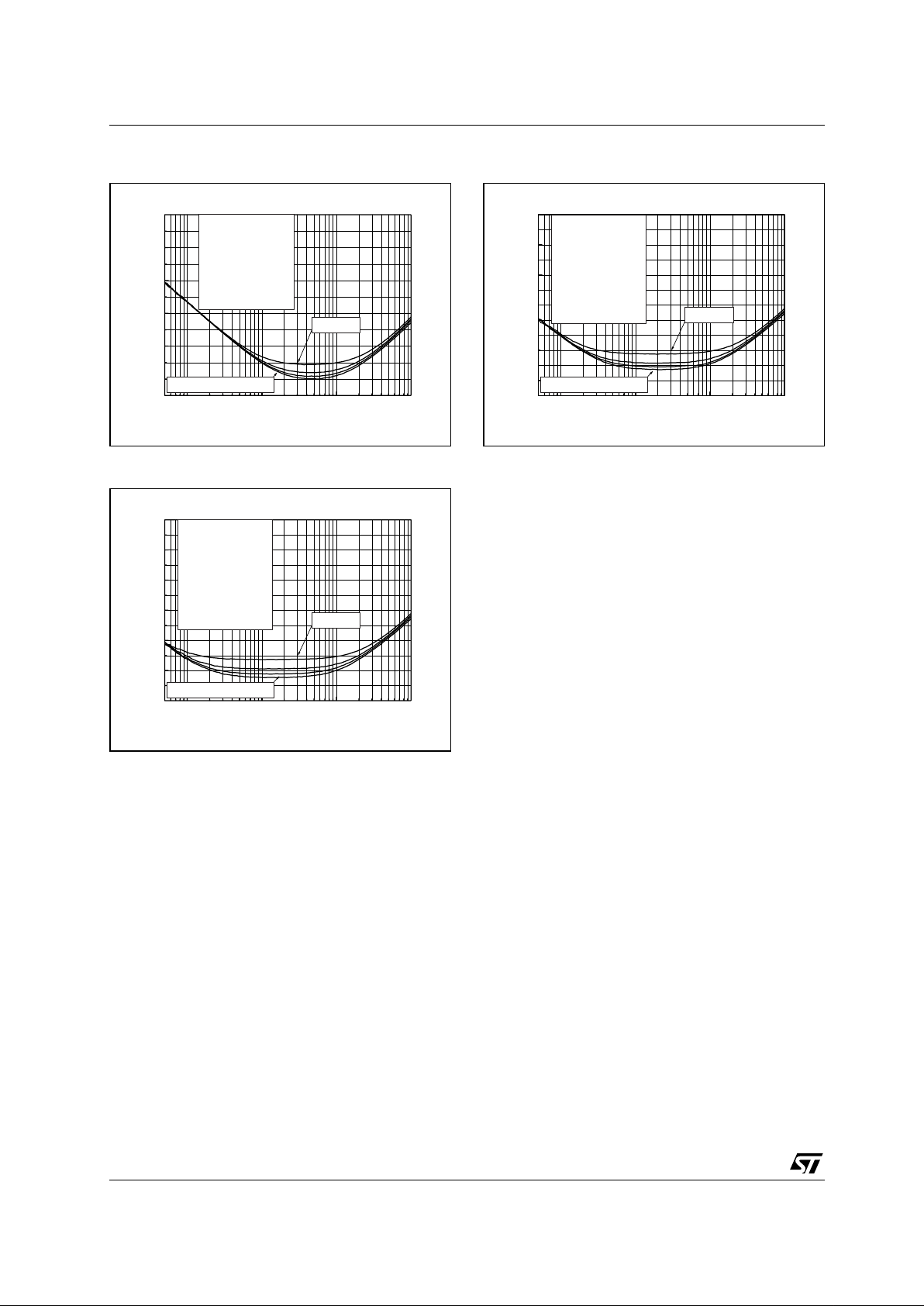
PACKAGE MECHANICAL DATA
DIM.
mm. inch
MIN. TYP MAX. MIN. TYP. MAX.
A 1.35 1.75 0.053 0.069
A1 0.10 0.25 0.04 0.010
A2 1.10 1.65 0.043 0.065
B 0.33 0.51 0.013 0.020
C 0.19 0.25 0.007 0.010
D 4.80 5.00 0.189 0.197
E 3.80 4.00 0.150 0.157
e 1.27 0.050
H 5.80 6.20 0.228 0.244
h 0.25 0.50 0.010 0.020
L 0.40 1.27 0.016 0.050
k ˚ (max.)
ddd 0.1 0.04
SO-8 MECHANICAL DATA
0016023/C
8

TS419-TS421
31/32
PACKAGE MECHANICAL DATA

TS419-TS421
32/32
PACKAGE MECHANICAL DATA
Information furnished is bel ieved to be accurate and reliable. However, STMicroe lectronics assumes no responsibility for the
consequences of use of such information nor for any infringement of patents or other rights of third parties which may result from
its use. No li cense is granted by implication or otherwise unde r any patent or patent rights of STMicroelectronics. Specifications
mentioned in this publication ar e subject to change without notice. This publication supersedes and replaces all information
previously supplied. S TMicroelectronics products are not authorized for use as critica l components in life suppo rt devices or
systems without express written approval of STMicroelectronics.
The ST logo is a registered trademark of STMicroelectronics
© 2003 STM icroelectronics - Pr inted in Ital y - All Rights Reserved
STMicr o el ectronics GROUP OF COMPANIES
Australi a - Brazil - Canada - Chin a - F i nl and - France - Germany - Hong Kong - Ind i a - Is rael - Ital y - J apan - Malaysia
Malta - Mor occo - Singapore - Spain - Sweden - Swi t zerland - U ni ted Kingdom - United Sta tes
http://www.st.com
 Loading...