

Datasheet TS420-700T, TS420-700H, TS420-700B, TS420-600T, TS420-600H Datasheet (SGS Thomson Microelectronics)
...
1/8
®
TS420 Series
SENSITIVE 4A SCRs
September 2000 - Ed: 3
MAIN FEATURES:
DESCRIPTION
Thanks to highly sensitive triggering levels, the
TS420 series is suitable for all applica tions where
the available gate current is limited, such as motor
control for hand tools, kitchen aids, overvoltage
crowbar protection for low power supplies, ...
Available in through-hole or surface-mount
packages, they provide an optimized performance
in a limited space area.
Symbol Value Unit
I
T(RMS)
4A
V
DRM/VRRM
600 and 700 V
I
GT
200 µA
ABSOLUTE RATINGS (lim iting values)
Symbol Parameter Value Unit
I
T(RMS)
RMS on-state current (180° conduction angle)
Tl = 115°C 4
A
IT
(AV)
Average on-state current (180° conduction angle)
Tl = 115°C 2.5
A
I
TSM
Non repetitive surge peak on-state
current
tp = 8.3 ms
Tj = 25°C
33
A
tp = 10 ms 30
I
²
tI
²
t Value for fusing
tp = 10 ms Tj = 25°C 4.5
A
2
S
dI/dt
Critical rate of rise of on-state current
I
G
= 2 x IGT , tr ≤ 100 ns
F = 60 Hz Tj = 125°C 50 A/µs
I
GM
Peak gate current tp = 20 µs Tj = 125°C 1.2 A
P
G(AV)
Average gate power dissipation Tj = 125°C 0.2 W
T
stg
Tj
Storage junction temperature range
Operating junction temp erature range
- 40 to + 150
- 40 to + 125
°C
G
A
K
DPAK
(TS420-B)
A
A
K
G
A
A
K
G
A
G
A
K
IPAK
(TS420-H)
TO-220AB
(TS420-T)
TS420 Series
2/8
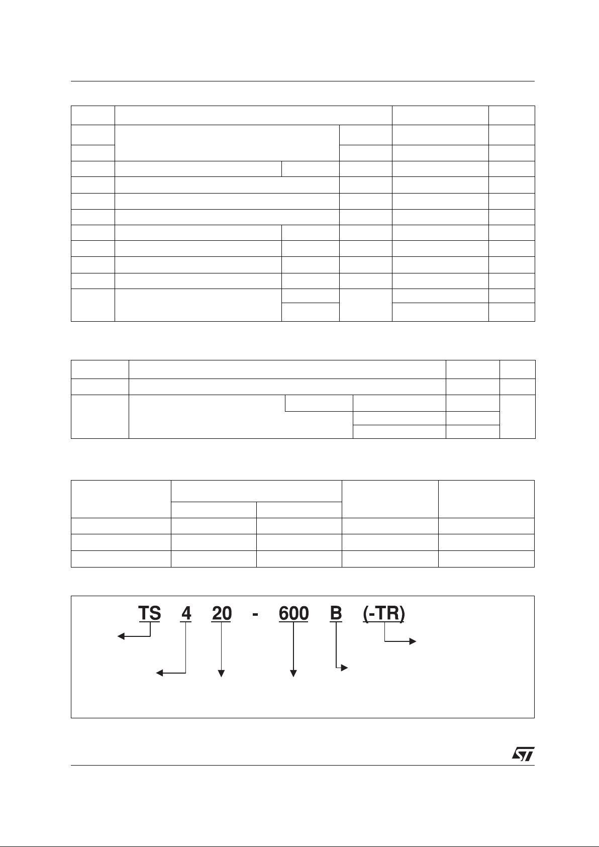
ELECTRICAL CHARACTERISTICS (Tj = 25°C, unless otherwise specified)
THERMAL RESISTANCES
S = copper s urface under tab
PRODUCT SELECTOR
ORDERING INFORMATION
Symbol Test Conditions TS420 Unit
I
GT
VD = 12 V RL = 33 Ω
MAX. 200
µA
V
GT
MAX. 0.8 V
V
GD
VD = V
DRM
RL = 3.3 kΩ RGK = 220 Ω
Tj = 125°C MIN.
0.1 V
V
RG
IRG = 10 µA
MIN.
8V
I
H
I
T
= 50 mA RGK = 1 kΩ
MAX. 5 mA
I
L
IG = 1 mA RGK = 1 kΩ
MAX. 6 mA
dV/dt
V
D
= 67 % V
DRM
RGK = 220 Ω
Tj = 125°C MIN. 5 V/µs
V
TM
ITM = 8 A tp = 380 µs
Tj = 25°C MAX. 1.6 V
V
t0
Threshold voltage Tj = 125°C MAX. 0.85 V
R
d
Dynamic resistance Tj = 125°C MAX. 90 mΩ
I
DRM
I
RRM
V
DRM
= V
RRM
RGK = 220 Ω
Tj = 25°C MAX. 5 µA
Tj = 125°C 1 mA
Symbol Parameter Value Unit
R
th(j-c)
Junction to case (DC)
3.0
°C/W
R
th(j-a)
Junction to ambient (DC)
S = 0.5 cm
²
DPAK 70
°C/W
IPAK 100
TO-220AB 60
Part Number
Voltage (xxx)
Sensitivity
Package
600 V 700 V
TS420-xxxB X X 200 µA DPAK
TS420-xxxH X X 200 µA IPAK
TS420-xxxT X X 200 µA TO-220AB
PACKING MODE
Blank:Tube
-TR: DPAK tape & reel
VOLTAGE:
600: 600V
700: 700V
SENSITIVITY:
20: 200µA
CURRENT: 4A
SCR
SERIES
PACKAGE:
B: DPAK
H: IPAK
T:TO-220AB
TS420 Series
3/8
OTHER INFORMATION
Note: x = voltage
Part Number Marking Weight Base Quantity Packing mode
TS420-x00B TS420x00 0.3 g 75 Tube
TS420-x00B-TR TS420x00 0.3 g 2500 Tape & reel
TS420-x00H TS420x00 0.4 g 75 Tube
TS420-x00T TS420x00T 2.3 g 50 Tube
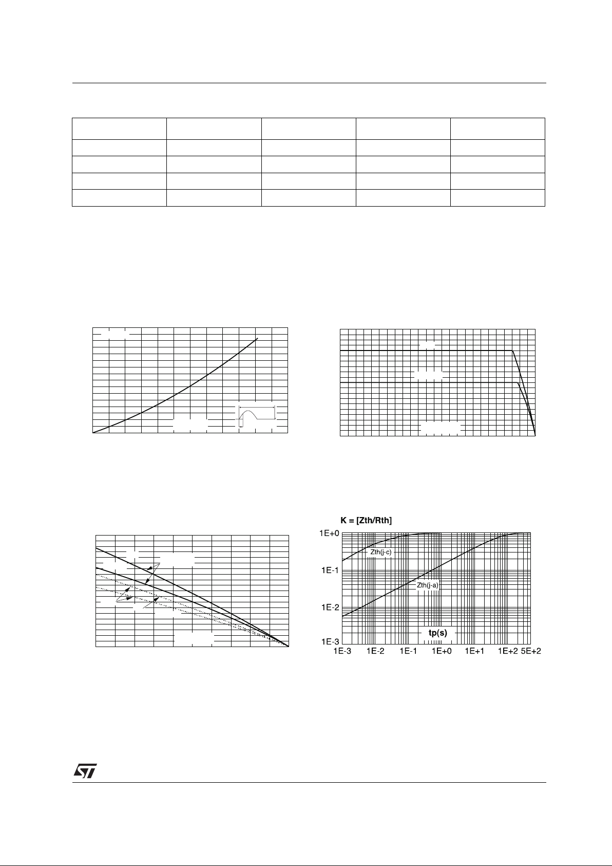
Fig. 1: Maximum average power dissipation
versus average on-state current.
Fig. 2-1: Average and D.C. on-state current
versus case temperature.
Fig. 2-2: Average and D.C. on-state current
versus ambient temperature (device mounted o n
FR4 with recommended pad layout) (DPAK).
Fig. 3: Relative variation of thermal impedance
junction to ambient versus pulse duration
(recommended pad layout, FR4 PC board) for
DPAK.
0.0 0.5 1.0 1.5 2.0 2.5 3.0
0.0
0.5
1.0
1.5
2.0
2.5
3.0
3.5
4.0
P(W)
α = 180°
IT(av)(A)
360°
α
0 25 50 75 100 125
0.0
0.5
1.0
1.5
2.0
2.5
3.0
3.5
4.0
4.5
5.0
IT(av)(A)
DC
α = 180°
Tcase(°C)
0 25 50 75 100 125
0.0
0.2
0.4
0.6
0.8
1.0
1.2
1.4
1.6
1.8
2.0
IT(av)(A)
α = 180°
DC
α = 180°
DPAK
(S = 0.5cm
2
)
IPA K
DC
Tamb( °C)

TS420 Series
4/8
Fig. 4: Relative variation of gate trigger current
and holding current versus junction temperature.
Fig. 5: Relative variation of holding current
versus gate-cathode resistance (typical values).
Fig. 6: Relative variation of dV/dt immunity
versus gate-cathode resistance (typical values).
Fig. 7: Relative variation of dV/dt immunity
versus gate-cathode resistance (typical values).
Fig. 8: Surge peak on-state current versus
number of cycles.
Fig. 9: Non-repetitive surge peak on-state
current for a sinusoidal pulse with width
tp < 10 ms, and corresponding values of I²t.
-40 -20 0 20 40 60 80 100 120 140
0.0
0.2
0.4
0.6
0.8
1.0
1.2
1.4
1.6
1.8
2.0
IGT,IH,IL [T j] / IG T,IH,IL [Tj = 25°C]
IGT
IH & IL
Rgk = 1kΩ
Tj(°C)
IH[Rgk] / IH[Rgk = 1k ]Ω
Rgk(kΩ)
0 0.2 0.4 0.6 0.8 1.0
1.2 1.4
1.6 1.8 2.0
0.01
0.10
1.00
10.00
Tj=125°C
VD=0.67xVDRM
dV/dt[Rgk] / dV/dt [Rgk = 220 ]Ω
Rgk(Ω)
0 2 4 6 8 10 12 14 16 18 20 22
0
2
4
6
8
10
VD = 0.67 x VDRM
Tj = 125°C
Rgk = 220Ω
dV/dt[Cgk] / dV/d t [R g k = 22 0 Ω]
Cgk(nF)
1 10 100 1000
0
5
10
15
20
25
30
35
ITSM(A)
Non repetitive
Tj initial = 25°C
Repetitive
Tcase = 115°C
Number of cycles
One cycle
tp = 10ms
0.01 0.10 1.00 10.00
1
10
100
300
ITSM(A),I2t(A2s)
Tj initial = 25°C
ITSM
I2t
dI/dt
limitattion
tp(ms)

TS420 Series
5/8
Fig. 10: On-state characteristics (maximum
values).
Fig. 11: Thermal resistance junct ion to ambient
versus copper surface under tab (Epoxy printed
circuit board FR4, copper thickness: 35 µm)
(DPAK).
0.0 0.5 1.0 1.5 2.0 2.5 3.0 3.5 4.0
0.1
1.0
10.0
50.0
ITM(A)
Tj max.:
Vto = 0.85V
Rd = 90mΩ
Tj = Tj max.
Tj = 25°C
VTM(V)
02468101214161820
0
20
40
60
80
100
Rth(j-a) ( °C/W)
S(cm2)

TS420 Series
6/8
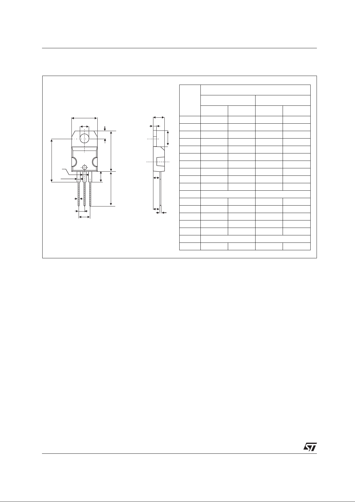
PACKAGE MECHANICAL DAT A
DPAK (Plastic)
REF.
DIMENSIONS
Millimeters Inches
Min. Max Min. Max.
A 2.20 2.40 0.086 0.094
A1 0.90 1.10 0.035 0.043
A2 0.03 0.23 0.001 0.009
B 0.64 0.90 0.025 0.035
B2 5.20 5.40 0.204 0.212
C 0.45 0.60 0.017 0.023
C2 0.48 0.60 0.018 0.023
D 6.00 6.20 0.236 0.244
E 6.40 6.60 0.251 0.259
G 4.40 4.60 0.173 0.181
H 9.35 10.10 0.368 0.397
L2 0.80 typ. 0.031 typ.
L4 0.60 1.00 0.023 0.039
R 0.2 typ. 0.007 typ.
V2 0° 8° 0° 8°
R
R
FOOTPRINT DIMENSIONS (in millimete r s )
DPAK (Plastic)
6.7
6.7
3
3
1.61.6
2.32.3

TS420 Series
7/8
PACKAGE MECHANICAL DAT A
IPAK (Plastic)
REF.
DIMENSIONS
Millimeters Inches
Min. Typ. Max. Min. Typ. Max.
A 2.2 2.4 0.086 0.094
A1 0.9 1.1 0.035 0.043
A3 0.7 1.3 0.027 0.051
B 0.64 0.9 0.025 0.035
B2 5.2 5.4 0.204 0.212
B3 0.85 0.033
B5 0.3 0.035
B6 0.95 0.037
C 0.45 0.6 0.017 0.023
C2 0.48 0.6 0.019 0.023
D 6 6.2 0.236 0.244
E 6.4 6.6 0.252 0.260
G 4.4 4.6 0.173 0.181
H 15.9 16.3 0.626 0.641
L 9 9.4 0.354 0.370
L1 0.8 1.2 0.031 0.047
L2 0.8 1 0.031 0.039
V1 10° 10°
H
L
L1
G
B5
B
V1
D
C
A1
A3
A
C2
B3
B6
L2
E
B2
TS420 Series
8/8
PACKAGE MECHANICAL DAT A
TO-220AB (Plastic)
REF.
DIMENSIONS
Millimeters Inches
Min. Max. Min. Max.
A 4.40 4.60 0.173 0.181
C 1.23 1.32 0.048 0.051
D 2.40 2.72 0.094 0.107
E 0.49 0.70 0.019 0.027
F 0.61 0.88 0.024 0.034
F1 1.14 1.70 0.044 0.066
F2 1.14 1.70 0.044 0.066
G 4.95 5.15 0.194 0.202
G1 2.40 2.70 0.094 0.106
H2 10 10.40 0.393 0.409
L2 16.4 typ. 0.645 typ.
L4 13 14 0.511 0.551
L5 2.65 2.95 0.104 0.116
L6 15.25 15.75 0.600 0.620
L7 6.20 6.60 0.244 0.259
L9 3.50 3.93 0.137 0.154
M 2.6 typ. 0.102 typ.
Diam. 3.75 3.85 0.147 0.151
A
C
D
L7
Dia
L5
L6
L9
L4
F
H2
G
G1
L2
F2
F1
E
M
Information furnished is believed to be accurate and reliable. However, STMicroelectronics assumes no responsibility for the consequences
of use of su ch in for mat i on n or f or a ny in fr ing em ent of pa te nts or o ther r igh ts of th ir d pa r tie s w hic h may res ul t f rom i ts us e. No license is granted
by impl i cation or otherwise un der any patent or patent rights of S T M i croelectroni cs. Specifi cations men tioned in this publicat ion are subject
to change wi t hout notice. Thi s publication su persedes and repl aces all inform ation previously supplied . S T M i croelectroni cs products are not
authori zed for use as cri tical components in life sup port devices or systems without express w ritten approval of STMicroelectronics.
© The ST logo is a registered trademark of STMicroelectronics
© 2000 STMicroelectronics - Printed in Italy - All Rights Reserved
STMicroele ct ronics GROUP OF COMP ANIES
Australi a - Brazil - China - Finland - France - Germany - Hong Kong - India - Italy - Japan - Malay sia - Malta - Morocco
Singapo re - Spain - Swe den - Switzerl and - United K i ngdom
http://ww w.st.com
 Loading...