

SGS Thomson Microelectronics TS4041CIZT-1.2, TS4041CIZ-1.2, TS4041-1.2, TS4041CILT-1.2, TS4041EIZT-1.2 Datasheet
...
1/9
■ 1.225V TYP OUTPUT VOLTAGE
■ UL TRA LOW OPERA TING CURRENT : 65µA
maximum at 25°C
■ HIGH PRECISION @ 25°C
+/- 2%
+/- 1%
+/- 0.5%
■ HIGH STABILITY WHEN USED WITH
CAP AC ITIVE LOADS
■ INDUSTRIAL TEMPERA TURE RANGE:
-40 to +85°C
■ 150ppm/°C MAXIMUM TEMPERATURE
COEFFICIENT
DESCRIPTION
The TS4041 is a low power shunt voltage
reference providing a stable 1.225V output
voltage over the industrial temperature range (-40
to +85°C). Availabe in SOT23-3 surface mount
package, it can be designed in applications where
space saving is a critical issue.
The low operating current is a key advantage for
power restricted designs. In add ition, the TS40 41
is very stable and can be used in a broad range of
application conditions.
APPLICATION
■ Computers
■ Instrumentation
■ Battery chargers
■ Switch Mode Power Supply
■ Battery operated equipments
ORDER CODE
Z = TO92 Plastic package - also available in Bulk (Z), Tape & Reel (ZT)
and Ammo Pack (AP)
LT = Tiny Package (SOT23-3) - only available in Tape & Reel (LT)
PIN CONNECTIONS (top view)
Precision TO92 SOT23-3
SOT23
Marking
2% TS4041EIZ-1.2 TS4041EILT-1.2 L233
1% TS4041DIZ-1.2 TS4041DILT-1.2 L232
0.5% TS4041CIZ-1.2 TS4041CILT-1.2 L231
Single temperature range: -40 to +85°C
Z
TO92
(Plastic Package)
L
SOT23-3L
(Plastic Micropacka ge)
TS4041
1.225V MICROPOWER SHUNT VOLTAGE REFERENCE
March 2002
TS4041
2/9
ABSOLUTE MAXIMUM RATINGS
OPERATING CONDITIONS
ELECTRICAL CHARACTERISTICS
TS4041E (2% Precision) T
amb
= 25°C (unless otherwise specified)
Symbol Parameter Value Unit
I
k
Reverse Breakdown Current 20 mA
I
f
Forward Current 10 mA
P
d
Power Dissipation
1)
SOT23-3
TO92
360
625
mW
T
std
Storage Temperature -65 to +150 °C
ESD Human Body Model (HBM) 2 kV
Machine Model (MM) 200 V
T
lead
Lead Temperature (solde ring, 10 second s) 260 °C
1. Pd has been ca l culated with T
amb
= 25°C and Tj = 150°C an d
Rthj a = 200°C/W for the TO92 package
Rthja = 340°C/W for the SOT23-3L package
Symbol Parameter Value Unit
I
min
Minimum Operating Current 65
µ
A
I
max
Maximum Operating Current 12 mA
T
oper
Operating Free Air Temperature Range -40 to +85 °C
Symbol Parameter Test Condition Min. Typ. Max. Unit
Vk
Reverse Breakdown Voltage
I
k
= 100µA
1.200 1.225 1.250 V
Reverse Breakdown Voltage Tolerance
I
k
= 100µA
-40°C < T
amb
< +85°C
-25
-36
+25
+36
mV
I
kmin
Minimum Operating Current
T
amb
= 25°C
40 65
µ
A
-40°C < T
amb
< +85°C
70
∆
V
ref
/∆T
Average Temperature Coefficient
Ik = 100µA
150 ppm/°C
∆
V
k
/∆I
k
Reverse Breakdown Voltage Change
with Operating Current Range
I
kmin
< Ik < 1mA
-40°C < T
amb
< +85°C
0.3 2
2.5
mV
1mA < I
k
< 12mA
-40°C < T
amb
< +85°C
2.5 8
10
R
ka
Static Impedance
∆
I
k
= 45µA to 1mA
0.25 0.5
Ω
K
vh
Long Term Stability
I
k
= 100µA, t = 1000hrs
120 ppm
En Wide Band Noise
I
k
= 100µA 10Hz < f < 10kHz
200 nV/√Hz
Note : Limits are 100% production tested at 25°C. Limits over temperature are guaranteed through correlation and by design.
TS4041
3/9
ELECTRICAL CHARACTERISTICS
TS4041D (1% Precision) T
amb
= 25°C (unless otherwise specified)
ELECTRICAL CHARACTERISTICS
TS4041C (0.5% Precision)T
amb
= 25°C (unless otherwise specified)
Symbol Parameter Test Condition Min. Typ. Max. Unit
Vk
Reverse Breakdown Voltage
I
k
= 100µA
1.213 1.225 1.237 V
Reverse Breakdown Voltage Tolerange
I
k
= 100µA
-40°C < T
amb
< +85°C
-12
-25
+12
+25
mV
I
kmin
Minimum Operating Current
T
amb
= 25°C
40 65
µ
A
-40°C < T
amb
< +85°C
70
∆
V
ref
/∆T
Average Temperature Coefficient
Ik = 100µA
150 ppm/°C
∆
V
k
/∆I
k
Reverse Breakdown Voltage Change
with Operating Current Range
I
kmin
< Ik < 1mA
-40°C < T
amb
< +85°C
0.3 2
2.5
mV
1mA < I
k
< 12mA
-40°C < T
amb
< +85°C
2.5 8
10
R
ka
Static Impedance
∆
I
k
= 45µA to 1mA
0.25 0.5
Ω
K
vh
Long Term Stability
I
k
= 100µA, t = 1000hrs
120 ppm
En Wide Band Noise
I
k
= 100µA 10Hz < f < 10kHz
200 nV/√Hz
Note : Limits are 100% production tested at 25°C. Limits over temperature are guaranteed through correlation and by design.
Symbol Parameter Test Condition Min. Typ. Max. Unit
Vk
Reverse Breakdown Voltage
I
k
= 100µA
1.219 1.225 1.231 V
Reverse Breakdown Voltage Tolerange
I
k
= 100µA
-40°C < T
amb
< +85°C
-6
-16
+6
+16
mV
I
kmin
Minimum Operating Current
T
amb
= 25°C
40 60
µ
A
-40°C < T
amb
< +85°C
65
∆
V
ref
/∆T
Average Temperature Coefficient
Ik = 100µA
120 ppm/°C
∆
V
k
/∆I
k
Reverse Breakdown Voltage Change
with Operating Current Range
I
kmin
< Ik < 1mA
-40°C < T
amb
< +85°C
0.3 1.5
2
mV
1mA < I
k
< 12mA
-40°C < T
amb
< +85°C
2.5 6
8
R
ka
Static Impedance
∆
I
k
= 45µA to 1mA
0.25 0.5
Ω
K
vh
Long Term Stability
I
k
= 100µA, t = 1000hrs
120 ppm
En Wide Band Noise
I
k
= 100µA 10Hz < f < 10kHz
200 nV/√Hz
Note : Limits are 100% production tested at 25°C. Limits over temperature are guaranteed through correlation and by design.
TS4041
4/9
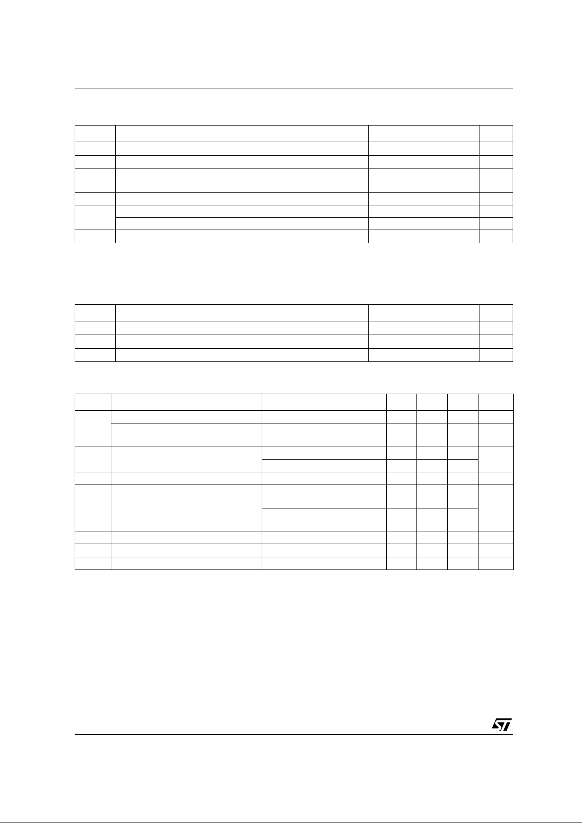
Reference voltage versus catho de current
Test circuit
Static impedance versus temperatu re
Reference voltage versus cathode current
Reference voltage versus Temperature
Noise voltage versus frequency
-1
-0.5
00.51
1.5
Reference voltage (V)
-8
-4
0
4
8
12
Cathode current (mA)
Ik=(Vin-Vref)/R
Vout=Vr ef
R
-40-200 20406080
Temperature ( °C )
0.2
0.21
0.22
0.23
0.24
0.25
Static impedance (Ohms)
-1
-0.5
0
0.5
1
1.5
Reference voltage (V)
-50
0
50
100
Cathode current (µA)
-40-200 20406080
T emperature (°C)
1.19
1.2
1.21
1.22
1.23
1.24
1.25
1.26
Cathode volta ge (V)
+0.5
%
-0.5%
-1%
+1%
-2 %
+2%
0 1 10 100 1,000 10,000
Frequency (kHz)
0
200
400
600
800
Noise voltage (nV/Hz)
CL=10µF
CL=0µF
CL=100µF

TS4041
5/9
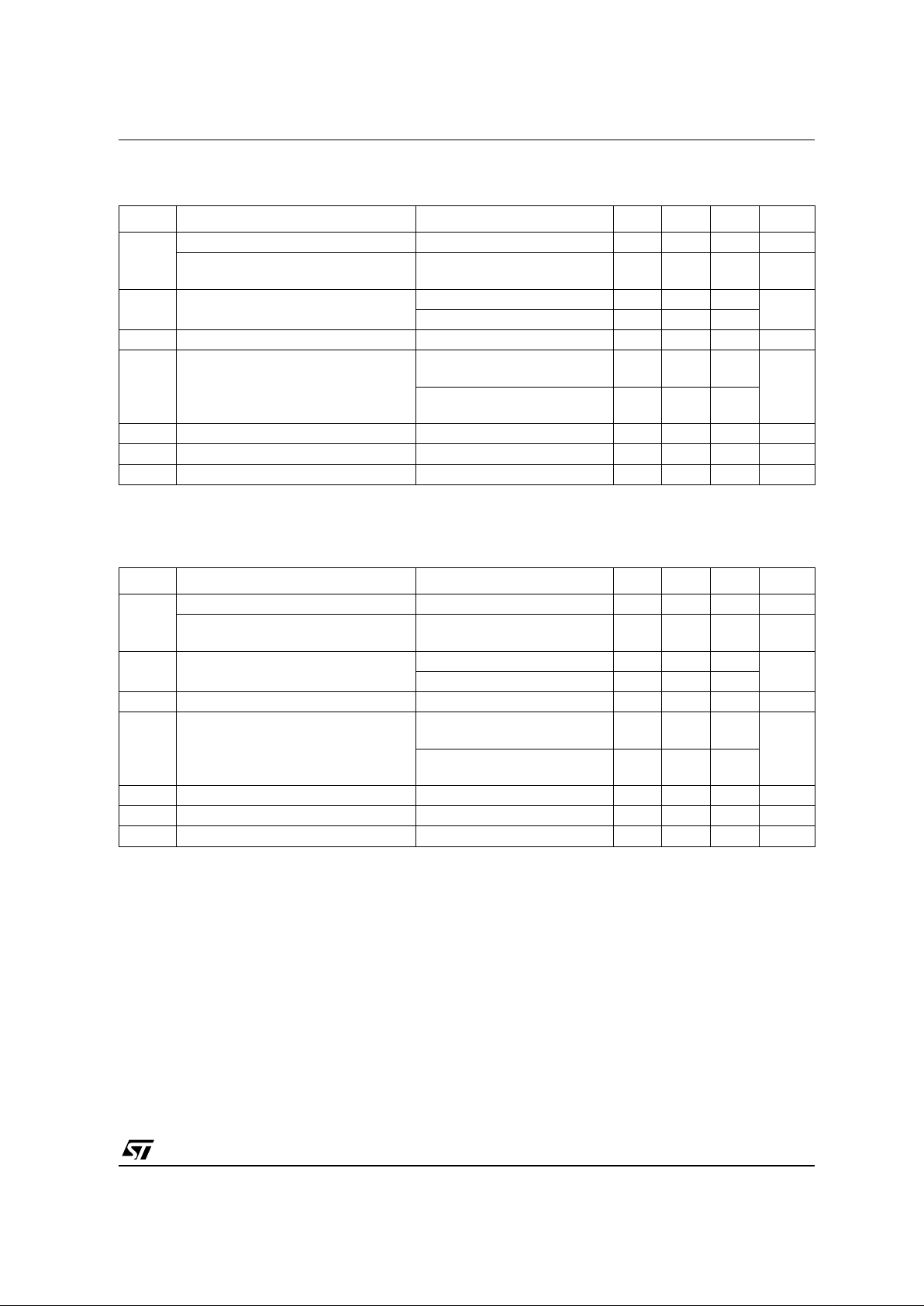
Pulse response for Ik=100µA
Pulse response for Ik=1mA
Test circuit for pulse response at Ik=100µA
Test circuit for pulse response at Ik=1mA
0246810
Time (µs)
3V
0V
1.225V
Input
Output
0V
024681
0
Time (µs)
3V
0V
1.225V
Input
Output
0V
Ik=100µA
Output
18 K
Ω
Pulse
Gen erator
Intput
Ik=1mA
Output
1.8 K
Ω
Pulse
Generator
Intput
TS4041
6/9
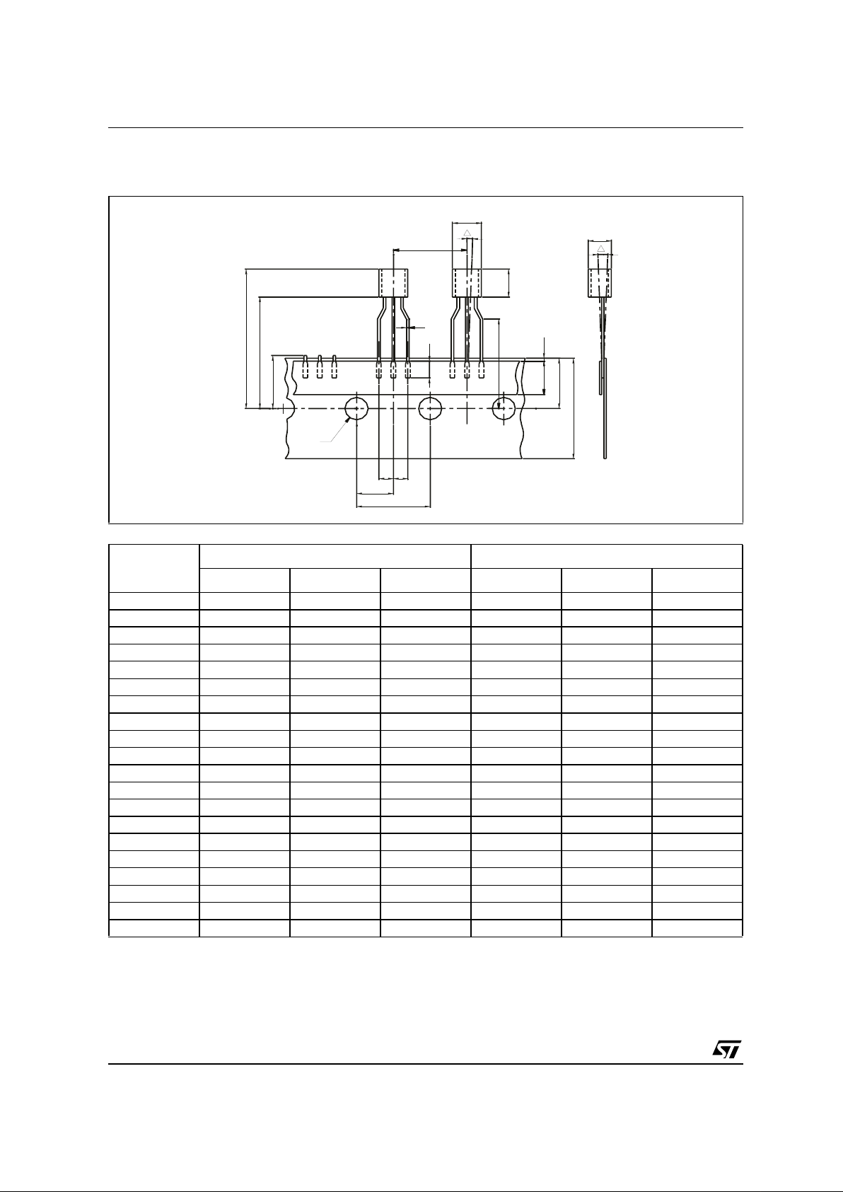
PACKAGE MECHANICAL DATA
3 PINS - PLASTIC PACKAGE TO92 (TAPE & REEL)
Dim.
Millimeters Inches
Min Typ. Max. Min. Typ. Max.
AL 5.0 0.197
A 5.0 0.197
T 4.0 0.157
d 0.45 0.018
I1 2.5 0.098
P 11.7 12.7 13.7 0.461 0.500 0.539
PO 12.4 12.7 13 0.488 0.500 0.512
P2 5.95 6.35 6.75 0.234 0.250 0.266
F1/F2 2.4 2.5 2.8 0.094 0.098 0.110
∆
h -1 0 1 -0.039 0 0.039
∆
P -1 0 1 -0.039 0 0.039
W 17.5 18.0 19.0 0.689 0.709 0.748
W0 5.7 6 6.3 0.224 0.236 0.248
W1 8.5 9 9.75 0.335 0.354 0.384
W2 0.5 0.020
H 20 0.787
H0 15.5 16 16.5 0.610 0.630 0.650
H1 25 0.984
DO 3.8 4.0 4.2 0.150 0.157 0.165
L1 11 0.433
A1
P
P
A
T
H
H1
H
L1
d
I1
H0
W2W0
W1
W
D0
F1
F2
P2
P0

TS4041
7/9
PACKAGE MECHANICAL DATA
3 PINS - PLASTIC PACKAGE TO92 (TAPE AMMO PACK)
Dim.
Millimeters Inches
Min Typ. Max. Min. Typ. Max.
AL 5.0 0.197
A 5.0 0.197
T 4.0 0.157
d 0.45 0.018
I1 2.5 0.098
P 11.7 12.7 13.7 0.461 0.500 0.539
PO 12.4 12.7 13 0.488 0.500 0.512
P2 5.95 6.35 6.75 0.234 0.250 0.266
F1/F2 2.4 2.5 2.8 0.094 0.098 0.110
∆
h -1 0 1 -0.039 0 0.039
∆
P -1 0 1 -0.039 0 0.039
W 17.5 18.0 19.0 0.689 0.709 0.748
W0 5.7 6 6.3 0.224 0.236 0.248
W1 8.5 9 9.75 0.335 0.354 0.384
W2 0.5 0.020
H 20 0.787
H0 15.5 16 16.5 0.610 0.630 0.650
H1 25 0.984
DO 3.8 4.0 4.2 0.150 0.157 0.165
L1 11 0.433
A1
P
P
A
T
H
H1
H
L1
d
I1
H0
W2W0
W1
W
D0
F1
F2
P2
P0

TS4041
8/9
PACKAGE MECHANICAL DATA
3 PINS - PLASTIC PACKAGE TO92 (BULK)
Dim.
Millimeters Inches
Min Typ. Max. Min. Typ. Max.
L 1.27 0.05
B 3.2 3.7 4.2 0.126 0.1457 0.1654
O1 4.45 5.00 5.2 0.1752 0.1969 0.2047
C 4.58 5.03 5.33 0.1803 0.198 0.2098
K 12.7 0.5
O2 0.407 0.5 0.508 0.016 0.0197 0.02
a 0.35 0.0138
TS4041
9/9
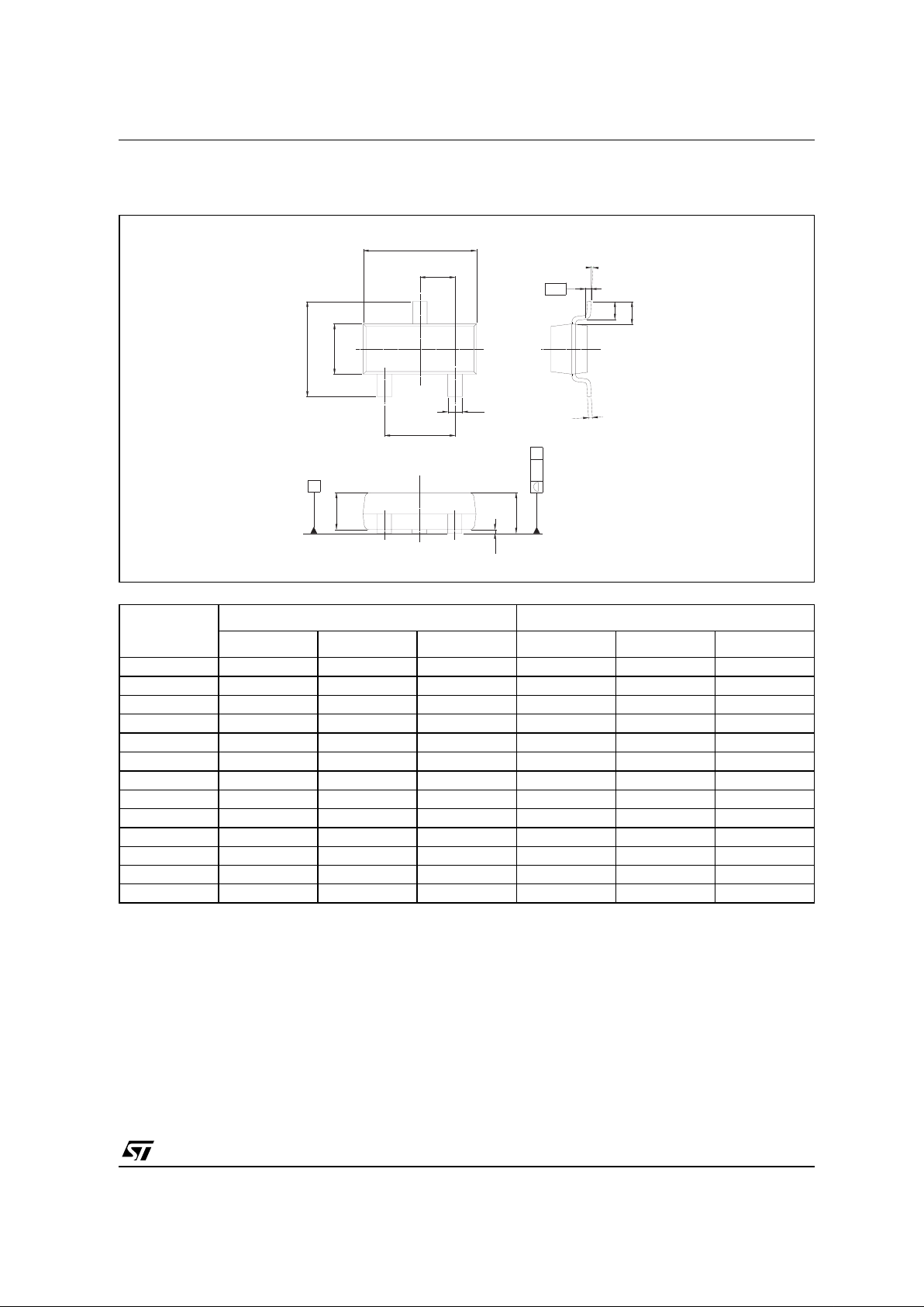
PACKAGE MECHANICAL DATA
3 PINS - TINY PACKAGE (SOT23)
Dimensions
Millimeters Inches
Min. Typ. Max. Min. Typ. Max.
A 0.890 1.120 0.035 0.044
A1 0.010 0.100 0.0004 0.004
A2 0.880 0.950 1.020 0.037 0.040
b 0.300 0.500 0.012 0.020
c 0.080 0.200 0.003 0.008
D 2.800 2.900 3.040 0.110 0.114 0.120
E 2.100 2.640 0.083 0.104
E1 1.200 1.300 1.400 0.047 0.051 0.055
e 0.950 0.037
e1 1.900 0.075
L 0.400 0.500 0.600 0.016 0.020 0.024
L1 0.540 0.021
k 0° 8°
A
A1
A2
D
e
e1
b
E
E1
0.10
C
C
SEATING
PLANE
L1
L
0.25
GAUGE
PLANE
c
k
Informat ion furnished is believed t o be accurate an d reliable. H owever, STMicr oelectronics assumes no responsibility for the
consequences of use of such information nor for any infringement of patents or other rights of third parties which may result from
its use. No license is granted by implication or otherwise under any patent or patent rights of STMicroelectronics. Specifica tions
mentioned in this publication are subject to change without notice. This publication superse des and replaces all information
previously supplied. STMicroelectronic s products are not authoriz ed for use as critical c omponents in life support dev ices or
systems without express written approval of STMicroelectronics.
© The ST logo is a registered trademark of STMicroelectronics
© 2002 STMicroelectronics - Printed in Italy - All Rights Reserved
STMicroelectronics GROUP OF C OM P AN IES
Australi a - B razil - Canada - China - Finland - Fran ce - Germany - Hong Kong - In di a - Israel - Ital y - Japan - Mal ays i a
Malta - Morocco - Singapore - Spain - Sweden - Switzerland - United Kingdom - United States
© http://www.st.com - United Kingdom
 Loading...