

Datasheet TS4040EIZT-2.5, TS4040EIZ-2.5, TS4040EILT-2.5, TS4040DIZT-2.5, TS4040DIZ-2.5 Datasheet (SGS Thomson Microelectronics)
...
1/10
■ 2.5V OUTPUT VOLTAGE
■ ULTRA LOW CURRENT CONSUMPTION:
40µA TYP.
■ HIGH PRECISION @ 25°C
±2% and ±1%
■ HIGH STABILITY WHEN USED WITH
CAP AC ITIVE LOAD
■ INDUSTRIAL TEMPERA TURE RANGE:
-40 to +85°C
■ 150ppm/°C MAXIMUM TEMPERATURE
COEFFICIENT
DESCRIPTION
The TS4040 is a low power shunt voltage reference providing a stable 2.5V output voltage over
the industrial temperature range (-40 to +85°C).
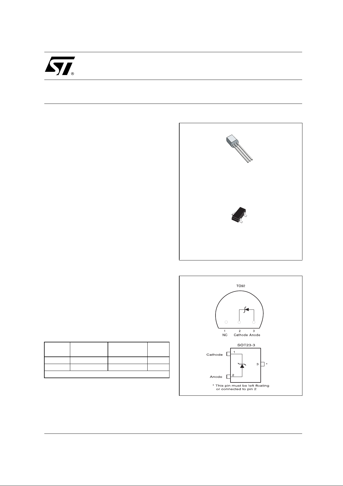
Available in SOT23-3 s urface mount package, it
can be designed in applications where space saving is a critical issue.
The low operating current is a key advantage for
power restricted designs. In add ition, the TS40 40
is very stable and can be used in a broad range of
application conditions.
APPLICATION
■ Computers
■ Instrumentation
■ Battery chargers
■ Switch Mode Power Supply
■ Battery operated equipments
ORDER CODE
Z = TO92 Plastic package - also available in Bulk (Z), T ape & Reel (ZT)
and Ammo Pack (AP)
LT = Tiny Package (SOT23-3) - only available in Tape & Reel (LT)
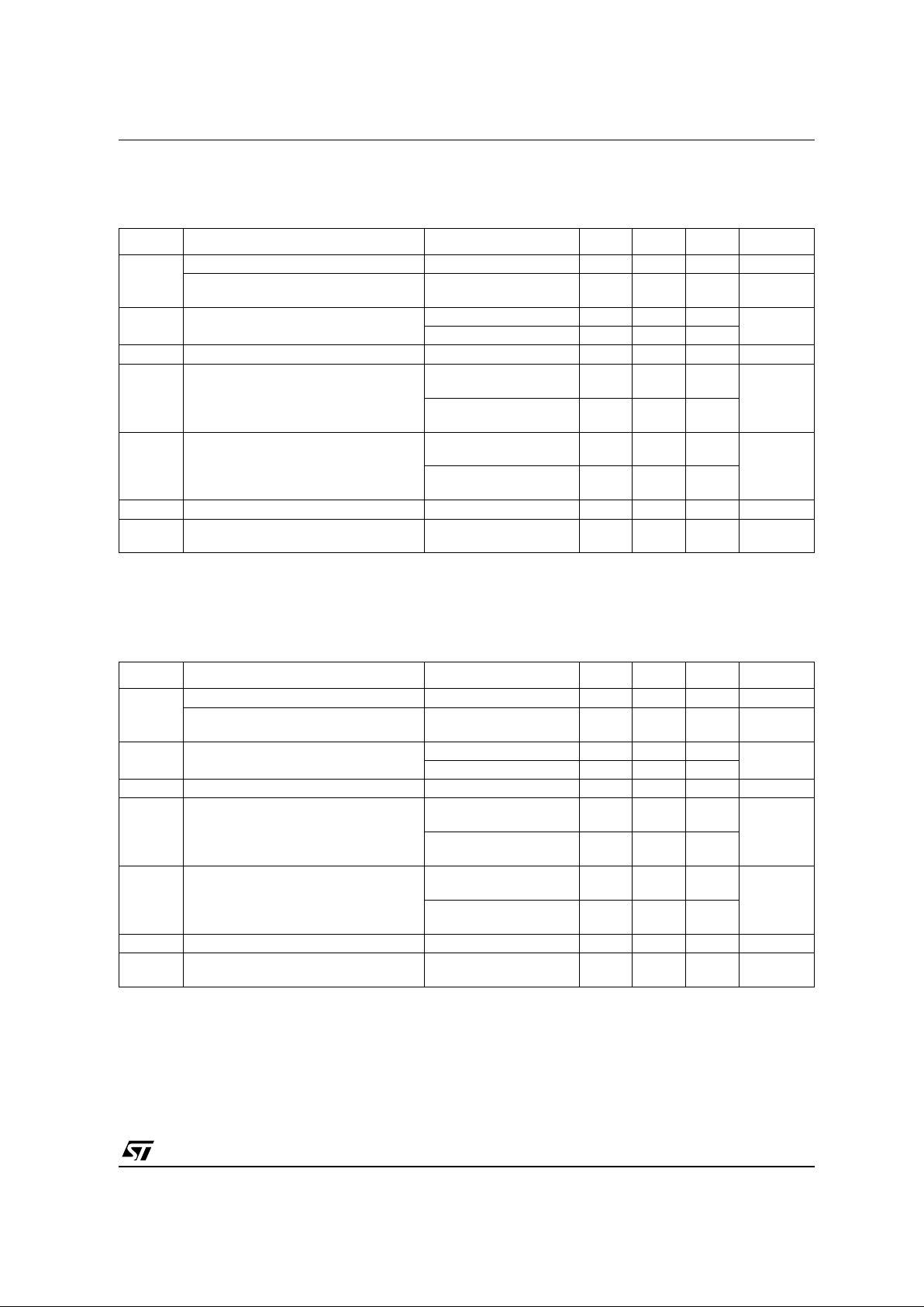
PIN CONNECTIONS (top view)
Precision TO92 SOT23-3
SOT23
Marking
2% TS4040EIZ-2.5 TS4040EILT-2.5 L243
1% TS4040DIZ-2.5 TS4040DILT-2.5 L242
Single temperature range: -40 to +85°C
Z
TO92
(Plastic Package)
L
SOT23-3L
(Plastic Micropacka ge)
TS4040
2.5V MICROPOWER SHUNT VOLTAGE REFERENCE
March 2002

TS4040
2/10
ABSOLUTE MAXIMUM RATINGS
OPERATING CONDITIONS
Symbol Parameter Value Unit
I
k
Reverse Breakdown Current 20 mA
I
f
Forward Current 10 mA
P
d
Power Dissipation
1)
SOT23-3
TO92
360
625
mW
T
std
Storage Temperature -65 to +150 °C
ESD Human Body Model (HBM) 2 kV
Machine Model (MM) 200 V
Tlead Lead Temperatue (soldering, 10 seconds) 260 °C
1. Pd has been ca l culated with Ta m b = 25°C, Tjunct i on =150°C andRthja = 200 °C/W for the TO92 package
Rthja = 340°C/W for the SOT23-3 package
Symbol Parameter Value Unit
I
kmin
Minimum Operating Current 60
µ
A
I
kmax
Maximum Operating Current 15 mA
T
oper
Operating Free Air Temperature Range -40 to +85 °C
TS4040
3/10
ELECTRICAL CHARACTERISTICS
TS4040E (2% Precision)
Tamb = 25°C (unless otherwise specified)
ELECTRICAL CHARACTERISTICS
TS4040D (1% Precision)
Tamb = 25°C (unless otherwise specified)
Symbol Parameter Test Condition Min. Typ. Max. Unit
Vk
Reverse Breakdown Voltage Ik = 100µA 2.45 2.5 2.55 V
Reverse Breakdown Voltage Tolerance
Ik = 100µA
-40°C < T < +85°C
-50
-74
50
74
mV
Ikmin Minimum Operating Current
T = 25°C 40 65
µ
A
-40°C < T < +85°C 70
∆
Vref/∆T Average Temperature Coefficient Ik = 100µA 30 150 ppm/°C
∆
Vk/∆Ik
Reverse Breakdown Voltage Change
with Operating Current Range
Ikmin < Ik < 1mA
-40°C < T < +85°C
0.4 1
1.2
mV
1mA < Ik < 15mA
-40°C < T < +85°C
2.5 8
10
Rka Reverse Static Impedance
Ik = Ikmin to 1mA
-40°C < T < +85°C
0.4 1
1.2
Ω
Ik = 1 to 15mA
-40°C < T < +85°C
0.2 0.6
0.7
Kvh Long Term Stability Ik = 100µA, t = 1000hrs 120 ppm
En Wide Band Noise
Ik = 100µA
10Hz < f < 10kHz
35
µ
Vrms
Note: Limits are 100% production tested at 25°C. Limits over temperature are guaranteed through correlation and by design.
Symbol Parameter Test Condition Min. Typ. Max. Unit
Vk
Reverse Breakdown Voltage Ik = 100µA 2.475 2.5 2.525 V
Reverse Breakdown Voltage Tolerance
Ik = 100µA
-40°C < T < +85°C
-25
-49
25
49
mV
Ikmin Minimum Operating Current
T = 25°C 40 65
µ
A
-40°C < T < +85°C 70
∆
Vref/∆T Average Temperature Coefficient Ik = 100µA 30 150 ppm/°C
∆
Vk/∆Ik
Reverse Breakdown Voltage Change
with Operating Current Range
Ikmin < Ik < 1mA
-40°C < T < +85°C
0.4 1
1.2
mV
1mA < Ik < 15mA
-40°C < T < +85°C
2.5 8
10
Rka Reverse Static Impedance
Ik = Ikmin to 1mA
-40°C < T < +85°C
0.4 1
1.2
Ω
Ik = 1mA to 15mA
-40°C < T < +85°C
0.2 0.6
0.7
Kvh Long Term Stability Ik = 100µA, t = 1000hrs 120 ppm
En Wide Band Noise
Ik = 100µA
10Hz < f < 10kHz
35
µ
Vrms
Note: Limits are 100% production tested at 25°C. Limits over temperature are guaranteed through correlation and by design.

TS4040
4/10
Reference voltage versus cathode current
-0.5 0 0.5 1 1.5 2 2.5
Cathode voltage (V)
-5
0
5
10
15
Cathode current (mA)
Test circuit
Vin
Ik=(Vin-Vref)/R
Vout=Vref
R
Static impedance (Rka) versus
temperature
-40 -20 0 20 40 60 80
Temperature (°C)
0
0.05
0.1
0.15
0.2
Static impedan ce ( O hms)
Minimum operating current
02040
Cathode cu rrent (µA)
0
0.5
1
1.5
2
2.5
3
Cathode voltage (V)
T=+85°C
T=-40°C
T=+25°C
-40-200 20406080
Temper ature ( °C)
2.42
2.44
2.46
2.48
2.5
2.52
2.54
2.56
2.58
Cathode voltage (V)
+2%
-2%
-1%
+1%
Noise voltage versus Frequency
0.1
1.0
10.0
100.0
1000.0
Frequency (KHz)
0
500
1000
1500
Noise voltage (n V/VH z)
CL=10µF
CL=0
CL=100µF
CL=100nF
CL=1µF

TS4040
5/10
Ik=100µA
Output
25k ohm
Pulse
Generator
Intput
Test circuit for pulse response at Ik=100µA
Pulse response for Ik=100µA
Detailed part
00.511.52
Time (µs)
0V
5V
2.5V
0V
Input
Output
Ik=1mA
Output
Pulse
Generator
Intput
Test circuit for pulse response at Ik=1mA
2.5k ohm
Pulse response for Ik=100µA
0
5
0
2.5
0 5 10 15 20
Time (µs)
Input
Output
Pulse response for Ik=100µA
Detailed part
012345
Time (µs)
0V
5V
0V
2.5V
Input
Output
Pulse response for Ik=1mA
0V
5V
0V
2.5V
012345
Time (µs)
Input
Output

TS4040
6/10
Pulse response for Ik=1mA
Detailed part
0V
5V
2.5
V
0V
0 50 100 150 200
Time ( ns)
Input
Output
Pulse response for Ik=1mA
Detailed part
0V
5V
0V
2.5V
0 0.2 0.4 0.6 0.8 1
Time (µs)
Input
Output

TS4040
7/10
PACKAGE MECHANICAL DATA
3 PINS - PLASTIC PACKAGE TO92 (TAPE & REEL)
Dim.
Millimeters Inches
Min Typ. Max. Min. Typ. Max.
AL 5.0 0.197
A 5.0 0.197
T 4.0 0.157
d 0.45 0.018
I1 2.5 0.098
P 11.7 12.7 13.7 0.461 0.500 0.539
PO 12.4 12.7 13 0.488 0.500 0.512
P2 5.95 6.35 6.75 0.234 0.250 0.266
F1/F2 2.4 2.5 2.8 0.094 0.098 0.110
∆
h -1 0 1 -0.039 0 0.039
∆
P -1 0 1 -0.039 0 0.039
W 17.5 18.0 19.0 0.689 0.709 0.748
W0 5.7 6 6.3 0.224 0.236 0.248
W1 8.5 9 9.75 0.335 0.354 0.384
W2 0.5 0.020
H 20 0.787
H0 15.5 16 16.5 0.610 0.630 0.650
H1 25 0.984
DO 3.8 4.0 4.2 0.150 0.157 0.165
L1 11 0.433
A1
P
P
A
T
H
H1
H
L1
d
I1
H0
W2W0
W1
W
D0
F1
F2
P2
P0

TS4040
8/10
PACKAGE MECHANICAL DATA
3 PINS - PLASTIC PACKAGE TO92 (TAPE AMMO PACK)
Dim.
Millimeters Inches
Min Typ. Max. Min. Typ. Max.
AL 5.0 0.197
A 5.0 0.197
T 4.0 0.157
d 0.45 0.018
I1 2.5 0.098
P 11.7 12.7 13.7 0.461 0.500 0.539
PO 12.4 12.7 13 0.488 0.500 0.512
P2 5.95 6.35 6.75 0.234 0.250 0.266
F1/F2 2.4 2.5 2.8 0.094 0.098 0.110
∆
h -1 0 1 -0.039 0 0.039
∆
P -1 0 1 -0.039 0 0.039
W 17.5 18.0 19.0 0.689 0.709 0.748
W0 5.7 6 6.3 0.224 0.236 0.248
W1 8.5 9 9.75 0.335 0.354 0.384
W2 0.5 0.020
H 20 0.787
H0 15.5 16 16.5 0.610 0.630 0.650
H1 25 0.984
DO 3.8 4.0 4.2 0.150 0.157 0.165
L1 11 0.433
A1
P
P
A
T
H
H1
H
L1
d
I1
H0
W2W0
W1
W
D0
F1
F2
P2
P0

TS4040
9/10
PACKAGE MECHANICAL DATA
3 PINS - PLASTIC PACKAGE TO92 (BULK)
Dim.
Millimeters Inches
Min Typ. Max. Min. Typ. Max.
L 1.27 0.05
B 3.2 3.7 4.2 0.126 0.1457 0.1654
O1 4.45 5.00 5.2 0.1752 0.1969 0.2047
C 4.58 5.03 5.33 0.1803 0.198 0.2098
K 12.7 0.5
O2 0.407 0.5 0.508 0.016 0.0197 0.02
a 0.35 0.0138

TS4040
10/10
PACKAGE MECHANICAL DATA
3 PINS - TINY PACKAGE (SOT23)
Dimensions
Millimeters Inches
Min. Typ. Max. Min. Typ. Max.
A 0.890 1.120 0.035 0.044
A1 0.010 0.100 0.0004 0.004
A2 0.880 0.950 1.020 0.037 0.040
b 0.300 0.500 0.012 0.020
c 0.080 0.200 0.003 0.008
D 2.800 2.900 3.040 0.110 0.114 0.120
E 2.100 2.640 0.083 0.104
E1 1.200 1.300 1.400 0.047 0.051 0.055
e 0.950 0.037
e1 1.900 0.075
L 0.400 0.500 0.600 0.016 0.020 0.024
L1 0.540 0.021
k 0° 8°
A
A1
A2
D
e
e1
b
E
E1
0.10
C
C
SEATING
PLANE
L1
L
0.25
GAUGE
PLANE
c
k
Information furnished is beli eved to be accurate and reliable. However, STMicroe lectronics assumes no responsibility for the
consequences of use of such information nor for any infringement of patents or other rights of third parties which may result from
its use. No licens e is granted by imp lication or otherwise under a ny patent or patent rig hts of STMicroelectronics. Specificat ions
mentioned in this publication ar e subject to change without notice. This publication supersedes and replaces all information
previously supplied. S TMicroelectronics products are not authorized for use as critica l components in life suppo rt devices or
systems without express written approval of STMicroelectronics.
© The ST logo is a registered trademark of STMicroelectronics
© 2002 STM i cr o electron ics - Printed in Italy - All Ri g h ts Reserved
STMicr oelectronics GROUP OF COMPANIES
Australi a - Brazil - Canada - China - F i nl and - France - Germany - Hong Kong - Indi a - Is rael - Italy - J apan - Malays i a
Malta - Mor occo - Singap ore - Spain - Sw eden - Switzerland - Unit ed Kingdom - Uni ted States
© http://www.st.com - United Kingdom
 Loading...